PCBA Meaning Simplified: A Beginner’s Guide to Printed Circuit Boards
Electronics are all around us, from smartphones to smart home devices, yet most people rarely consider what makes these devices actually work. At the heart of every functioning gadget lies a Printed Circuit Board Assembly (PCBA) — a carefully arranged network of circuits and components that brings a design to life. Understanding what PCBA means, how it’s built, and why it matters can demystify the electronics in your hands and give you the confidence to explore, create, or even troubleshoot your own projects.
Introduction to PCBA
Understanding the basics of PCBA is essential for anyone interested in electronics, whether you’re a hobbyist, student, or professional engineer. A solid grasp of what PCBA involves lays the foundation for designing, assembling, and troubleshooting electronic devices effectively.
Definition of PCBA
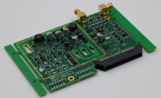
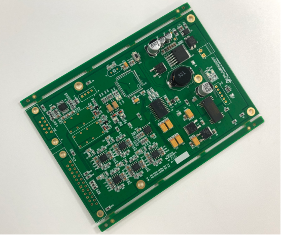
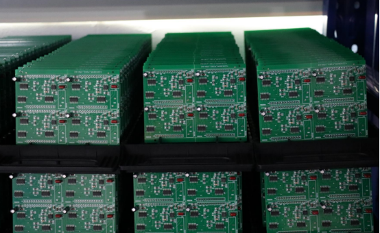
PCBA stands for Printed Circuit Board Assembly. It refers to a PCB (Printed Circuit Board) that has been populated with electronic components such as resistors, capacitors, integrated circuits (ICs), LEDs, and connectors.
The main difference between a PCB and a PCBA is that a PCB is simply the bare board with copper traces, while a PCBA is a fully functional unit ready to perform its intended electrical task.
Example: A blank PCB for a small sensor module becomes a working PCBA once components like a microcontroller, resistors, and connectors are soldered onto it. This transformation turns a simple board into an operational part of a circuit.
Importance of Understanding PCBA
Grasping what PCBA is and how it functions is critical in several areas:
- Electronics manufacturing: PCBA knowledge helps engineers and technicians ensure devices are built correctly and meet quality standards.
- Prototyping: Hobbyists and designers can create functional prototypes, test circuits, and iterate designs more efficiently.
- Troubleshooting and repairs: Knowing the structure of a PCBA allows users to identify faulty components or incorrect connections quickly.
Example: If a device isn’t working, understanding the PCBA layout helps locate a misaligned IC or a solder bridge, enabling faster repairs or modifications.
Components of a PCBA
A PCBA is composed of three main elements: the base PCB, the electronic components mounted on it, and the method used to assemble them. Understanding each part is crucial for designing, building, or troubleshooting electronic devices.
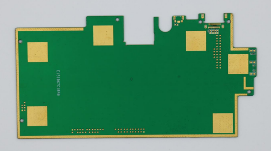
The Printed Circuit Board (PCB)
The PCB forms the foundation of a PCBA, providing mechanical support and electrical connections.
Base Material Types:
- FR-4: Standard fiberglass material, widely used for rigid boards.
- CEM-1: Paper-based material, less expensive, suitable for simple circuits.
- Flexible boards: Thin, bendable substrates for wearable devices or compact electronics.
Electrical Pathways:
- Copper traces: Carry electrical signals between components.
- Pads: Points where components are soldered.
- Vias: Holes that connect copper layers in multi-layer PCBs.
Electronic Components
Components are mounted on the PCB to make it functional.
Common Components:
- Resistors, capacitors, inductors – control current and voltage.
- Integrated Circuits (ICs) – perform logic or processing tasks.
- LEDs, connectors, switches – interface with the environment or user.
Categorization:
- Passive components: Do not generate power (resistors, capacitors).
- Active components: Can control current or amplify signals (transistors, ICs).
Example: Placement affects functionality—placing a capacitor too far from its associated IC may reduce filtering efficiency, causing signal noise.
Assembly Methods
Components are mounted onto the PCB using specific assembly techniques.
Through-Hole Mounting:
Component leads are inserted into drilled holes and soldered underneath.
- Advantages: Strong mechanical bond, easy for prototyping.
- Disadvantages: Slower, uses more space on the board.
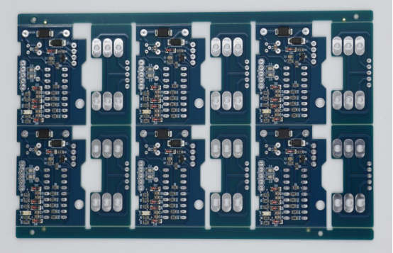
Surface-Mount Technology (SMT):
Components are placed directly on the PCB surface and soldered, usually via reflow soldering.
- Advantages: Smaller components, higher component density, automated assembly.
- Disadvantages: Harder to repair manually, requires precise machinery.
Comparison Example: Hobbyists may prefer through-hole for small DIY projects, while modern smartphones rely on SMT for compact, high-density designs.
PCBA Manufacturing Process
The PCBA manufacturing process transforms a bare PCB and loose electronic components into a fully functional assembly. Understanding each step helps beginners and professionals design, build, and troubleshoot electronics effectively.
Design and Layout
- The first step in PCBA production is designing the circuit and PCB layout.
- Engineers create a schematic diagram to define how components connect electrically.
- PCB layout tools, such as Eagle, KiCAD, or Altium, convert the schematic into a physical board design with traces, pads, and vias.
Example: A simple LED blink circuit schematic is transformed into a PCB layout where each LED, resistor, and microcontroller has an exact placement on the board.
This step ensures the board will be functional, manufacturable, and compatible with the chosen components.
Component Sourcing and Preparation
Once the design is finalized, components must be sourced and prepared:
- Select components with correct part numbers, specifications, and ratings.
- Test sensitive components like ICs or LEDs before assembly to ensure functionality.
- Organize components according to placement on the board to streamline the assembly process.
- Proper sourcing prevents assembly errors and reduces the risk of defective PCBA.
Assembly Techniques
Components are attached to the PCB using different assembly methods:
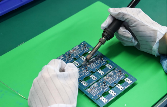
Manual Soldering vs. Automated Pick-and-Place Machines:
- Manual soldering is suitable for prototyping or low-volume production.
- Automated pick-and-place machines place SMT components rapidly and accurately for mass production.
Reflow Soldering (for SMT components):
- Solder paste is applied to pads, components are positioned, and the board is heated in a reflow oven to melt the solder and secure components.
Wave Soldering (for Through-Hole components):
- The board passes over molten solder, which attaches leads to pads simultaneously.
Comparison Example: A hobbyist kit may use manual soldering for a small SMT board, whereas a smartphone manufacturer relies on fully automated pick-and-place and reflow soldering for thousands of boards per day.
Testing and Quality Control
After assembly, the PCBA undergoes testing to ensure reliability:
- Electrical Testing: Checks for continuity, shorts, and proper circuit functionality.
- Visual Inspection: Ensures components are properly placed and soldered.
- Automated Optical Inspection (AOI): Uses cameras to detect misaligned, missing, or defective components.
Example: A misaligned microcontroller pin causing a malfunction can be detected via AOI and corrected before shipping.
Thorough testing and quality control are critical to delivering functional, high-quality PCBAs.
Common Applications of PCBA
Printed Circuit Board Assemblies (PCBAs) are the backbone of nearly all modern electronic devices. Understanding their common applications helps beginners, engineers, and hobbyists see how these assemblies are used in real-world scenarios.
Consumer Electronics
- Smartphones, laptops, and tablets: PCBAs integrate processors, memory, sensors, and connectivity modules to make devices functional.
- Home appliances: Microwaves, washing machines, and smart TVs rely on PCBAs to control user interfaces, sensors, and operational logic.
Example: A smartphone PCBA combines the main processor, battery management circuits, and wireless communication modules in a compact board.
Consumer electronics benefit from high-density PCBA designs to save space and support complex functionalities.
Industrial Electronics
- Programmable Logic Controllers (PLCs): PCBAs manage automation and control in factories and industrial machines.
- Control systems: Motor controllers, conveyor systems, and robotic arms use PCBAs to process signals and commands.
- Sensors: Temperature, pressure, and flow sensors rely on PCBAs for signal conditioning and communication.
Industrial PCBAs often prioritize durability and reliability, as devices must withstand harsh operating conditions.
Automotive and IoT Devices
- Electronic Control Units (ECUs): PCBAs in cars control engine functions, braking systems, and infotainment.
- Wearable devices: Smartwatches and fitness trackers rely on small, flexible PCBAs for processing and connectivity.
- Connected sensors: IoT devices in homes and cities use PCBAs to collect and transmit data.
Automotive and IoT PCBAs emphasize compact design, low power consumption, and high reliability for long-term operation.
Advantages of Understanding PCBA
Knowing how PCBA works offers tangible benefits for hobbyists, engineers, and anyone involved with electronics. From DIY projects to professional product development, understanding PCBA improves efficiency, accuracy, and creativity.
For Hobbyists and Makers
- DIY projects and prototyping: Knowledge of PCBA enables hobbyists to assemble, modify, and test electronic circuits confidently.
- Repairs: Understanding PCBA structure allows users to identify faulty components and replace them without professional help.
Example: A maker can repair a malfunctioning Arduino shield by recognizing which IC or capacitor is causing a short circuit.
For Engineers and Professionals
- Troubleshooting: Engineers can quickly locate design flaws or assembly defects on a PCBA.
- Design optimization: Knowing component placement, soldering methods, and trace layout improves circuit performance.
- Product development: PCBA expertise helps professionals reduce development time and ensure reliable, manufacturable designs.
Example: Adjusting the placement of decoupling capacitors on a high-speed PCBA can reduce electromagnetic interference (EMI).
Cost and Time Benefits
- Understanding PCBA reduces assembly errors and component wastage, lowering production costs.
- Speeds up prototyping cycles by minimizing trial-and-error iterations.
- Improves yield and product quality by catching potential issues early in design or assembly.
Example: A small company producing custom IoT devices can save hundreds of dollars by preventing PCB miswiring before mass production.
Common PCBA Issues and Troubleshooting
Even well-designed PCBAs can encounter issues during assembly or operation. Identifying and resolving these problems quickly is key to maintaining device performance and reliability.
Soldering Problems
- Cold joints: Occur when solder does not fully melt or adhere, causing intermittent electrical connections.
- Bridging: Excess solder creates unwanted connections between adjacent pads or pins.
- Component misalignment: Parts are not correctly positioned on the pads, which can cause malfunction.
Example: A misaligned IC on a microcontroller board may prevent proper signal routing, causing the device to fail intermittently.
Component Failures
- Overheating: Components damaged by excessive soldering heat or operational load.
- Polarity errors: Incorrect orientation of polarized components like diodes or electrolytic capacitors.
- Wrong ratings: Using a resistor or capacitor with inappropriate specifications can lead to circuit failure.
Example: Installing a 10µF capacitor instead of a 100µF in a power supply section may result in voltage instability.
Design-Related Issues
- Trace errors: Broken or incorrectly routed traces can interrupt signal flow.
- Insufficient spacing: Pads or traces too close together increase the risk of shorts or EMI issues.
- Wrong footprint: Component footprint mismatch prevents proper placement and soldering.
Example: An IC footprint that doesn’t match the actual package may require rework or board redesign.
Solutions and Best Practices
- Inspection: Use visual inspection or automated optical inspection (AOI) to identify soldering or placement errors.
- Testing: Perform continuity tests, functional tests, and check for shorts before powering the board.
- Corrective measures: Rework cold joints, replace failed components, or adjust design layouts for better spacing.
-
Step-by-step tip:
1 . Power off the board.
2. Inspect visually for misaligned components or solder bridges.
3. Test electrical continuity between critical points.
4. Resolder or replace defective components as needed.
By proactively inspecting and testing PCBAs, you can reduce defects, improve reliability, and avoid costly rework in both prototypes and production boards.
Conclusion
Understanding PCBA (Printed Circuit Board Assembly) is essential for anyone working with electronics. A PCBA transforms a bare PCB into a functional circuit by combining components, layout design, and proper assembly techniques. This knowledge helps beginners, hobbyists, and professionals design, troubleshoot, and optimize electronic devices efficiently.
For those just starting, it’s best to begin with small projects, practice assembly and testing, and gradually take on more complex circuits. Hands-on experience is the most effective way to gain confidence and mastery in working with PCBAs.
If you have further questions or want to learn more about PCBA, feel free to contact PCBMASTER . As a professional PCBA supplier, PCBMASTER can provide expert guidance, technical advice, and reliable solutions for your electronics projects.
FAQs
| Question | Answer |
|---|---|
| What is the difference between a PCB and a PCBA? | A PCB (Printed Circuit Board) is a bare board with copper traces, pads, and vias but no components. A PCBA (Printed Circuit Board Assembly) is a PCB populated with electronic components like resistors, capacitors, ICs, LEDs, and connectors, making it a functional circuit. Example: A blank sensor PCB becomes a PCBA when components are soldered on. |
| How do through-hole and surface-mount assembly differ in practice? | Through-hole: Component leads go through drilled holes and are soldered underneath. Strong mechanical bond, slower assembly, larger footprint. SMT: Components placed directly on the PCB surface and soldered (often by reflow). Supports high-density boards, faster for automation, harder to repair manually. Example: Hobbyist kits often use through-hole; smartphones rely on SMT. |
| Can a beginner assemble a PCBA at home safely? | Yes, if proper precautions are followed: use low-voltage kits, wear safety goggles, work in a ventilated area, and start with simple PCBA kits. Example: Assembling an Arduino shield or LED project kit at home is safe with these practices. |
| What tools are essential for testing a PCBA? | Key tools include: multimeter (voltage, current, continuity), oscilloscope (signal waveforms), test probes/clips, and magnifying glass or AOI (detect soldering issues and misplacements). Example: A multimeter can verify trace continuity before powering the board. |
| How does PCBA quality affect the lifespan of electronic devices? | High-quality PCBAs with correct soldering, proper placement, and accurate design improve device reliability and lifespan. Poor-quality PCBAs can cause failures, overheating, or early component damage. Example: A smartphone with a well-made PCBA lasts years, while one with cold solder joints may fail within months. |
About the Author

Carol Luo
PCB Design EngineerI'm Carol, a PCB Engineer at PCBMASTER with experience in PCB design and manufacturing engineering since 2018. I focus on translating engineering requirements into reliable PCB solutions, with expertise in stack-up design, material selection, and design-for-manufacturing (DFM). I share practical engineering insights from real-world PCB design and production experience.
Visit Carol Luo's Profile