


PCB Single Board vs Panelization Key Differences and Considerations
Introduction
Meta Description: Struggling to choose between single PCB and panelization for prototyping? This guide explains the definitions, differences, pros, cons, and use cases of single PCBs and panels in an easy-to-understand way. Make the best cost and quality decisions to improve production efficiency.
Introduction: Start with a Simple Story
Imagine you're a talented baker who has designed a delicious cookie. Now, you need to produce it. You have two choices:
·Bake Individually: Bake one cookie at a time. Precise control, but highly inefficient and wastes oven space.
·Bake on a Sheet: Place multiple cookie dough pieces on a large tray and bake them all at once. Highly efficient, saves energy, but you need to break them apart after baking.
This simple analogy perfectly illustrates the core difference between "Single Boards" and "Panelization" in PCB manufacturing. Today, we'll thoroughly understand these two concepts so you can make informed decisions in your PCB design and production.
Chapter 1: Basic Concepts - What is a PCB Single Board? What is PCB Panelization?
PCB Single Board
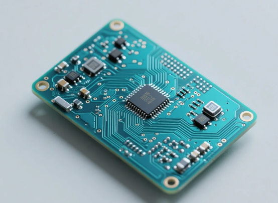
Definition: Refers to manufacturing where each PCB is independent, completely separate from others. Like the "individually baked cookie" in our analogy.
Characteristics:
·The production files (Gerber) sent to the board factory contain only one circuit board unit.
·On the production line (SMT assembly line), boards need to be loaded, assembled, and soldered one by one.
Typically used for prototype verification, small-batch production, or very large boards.
PCB Panelization
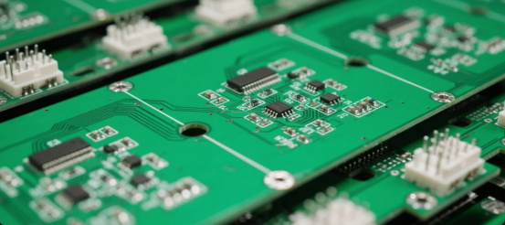
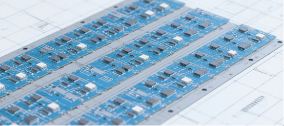
Definition: Refers to combining multiple identical PCB units (or different units) regularly onto a large panel for collective production and processing. After manufacturing, depanelization methods are used to separate PCBs into individual PCBs. Proper spacing between adjacent boards is important to ensure clean separation and prevent damage. These are the “cookies baked on a sheet.”
Why is Panelization Needed? Primarily to adapt to the automated equipment of modern electronics manufacturing. SMT pick-and-place machines have fixed-width conveyors that handle large panels. Using single small boards would be incredibly inefficient.
Two Main Panelization Methods:
·V-Scoring (V-Cut):
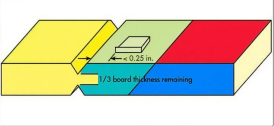
A V-shaped blade cuts shallow v-shaped grooves (v groove, v grooves) between adjacent boards on the panel, removing a specific portion of the board's thickness. This facilitates easy separation while maintaining structural integrity for the remaining material. After assembly, they are easily broken apart like chocolate bars. Suitable for regular shapes (squares/rectangles).
·Break-away Tabs (Mouse Bites):
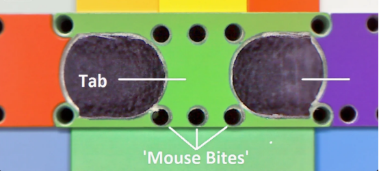
Small perforated holes connect the boards around the edges or between units, with small tabs remaining. Depaneling requires snapping by hand or cutting with tools. Extra support, such as breakaway rails or braces, may be needed in the panel, especially for larger or irregularly shaped boards.
When designing the panel, consider component placement and surface stress to avoid damage to components during depanelization. Depanelization methods include the use of a depaneling router, which provides precise, automated separation of individual PCBs.
Chapter 2: In-Depth Comparison - 5 Key Differences Between Single Boards and Panels
For a quick overview, here is a comparative table:
| Aspect | PCB Single Board | PCB Panelization |
|---|---|---|
| Production Efficiency | Very low, requires individual loading/unloading | Very High, processes entire panel at once |
| Production Cost | Low panel material utilization, SMT cost charged per board, higher total cost | High panel material utilization, SMT cost charged per panel, lower unit cost |
| Manual SMT | 0603~DIP | ±0.3mm |
| Suitable Scenarios | Prototypes, samples, small batches, very large boards | Standard choice for medium to large volume production |
| Process Requirements | No need for depaneling design | Requires V-Score or Break-away Tab design, tests design skills |
| Product Quality | Zero depaneling stress, no potential damage | Depaneling process generates stress, may damage components |
Production Efficiency & Cost: The Absolute Advantage of Panelization
This is the core purpose of panelization. A significant part of an SMT assembly house’s cost is the “engineering fee” or “setup cost,” which is a fixed expense. The machine must be set up whether it’s for 1 board or 100 boards(PCB Manufacturer & PCB Assembly services - Online PCB Quote. - PCBMASTER).
·Single Board: Assembling 100 single boards requires the machine to be set up 100 times, incurring 100 engineering fees. Highly inefficient.
·Panelization: If you panelize 10 boards onto one large panel, assembling 100 boards only requires 10 machine setups (10 large panels), reducing the engineering fee cost by a factor of 10! For medium to large production runs, panelization saves significant money.
PCBs are manufactured by cutting them from large sheets of laminate (e.g., 36 inches x 48 inches).
·Single Board: If your board shape is irregular, nesting single boards directly may leave large blank areas on the laminate sheet, wasting material.
·Panelization: Through clever arrangement, like a game of Tetris, you can maximize the use of the entire laminate sheet, minimizing waste and further reducing the material cost per board.
Application Scenarios: Each Has Its Role
Choose Single Boards When:
·You are doing initial concept verification (prototyping): You only need one or two boards; speed is key, and cost difference is minimal.
·Your board is very large: e.g., server motherboards, large control boards, which are already standard large panels.
·The production volume is very small: Only producing a few dozen pieces; the savings from panelization might not outweigh the design and depaneling costs.
Choose Panelization When:
·You are moving to medium or large volume production (this is the standard): All consumer electronics (phones, headphones, routers) use panelized boards.
·Your board is small or has an irregular shape: It must be panelized to fit SMT equipment.
·You want to optimize cost: This is the primary reason panelization exists.
Panelization is especially advantageous for mass production, as it streamlines manufacturing, increases efficiency, and reduces costs when producing large quantities of boards.
Process & Quality: The Hidden Advantage of Single Boards
·Process(About Us - One-Stop PCBA Manufacturer Introduction - PCBMASTER): Single boards require almost no additional process design. Panelization requires engineers to carefully design the V-Score path and depth or the location and number of break-away tabs—it’s a technical skill. It is important to follow the following design considerations when planning panelization, such as PCB strength, component layout, shape, tooling holes, score lines, component spacing, and handling irregular shapes, to ensure manufacturability and minimize depanelization stress.
·Quality: This is the only area where single boards potentially “outperform” panels. The depaneling process, whether manual breaking or using a depaneling machine, imposes mechanical stress on the PCB. If the board has very fragile, vibration-sensitive components (like large BGAs, crystals), this stress could cause internal micro-cracks, affecting long-term reliability. Single boards completely avoid this issue.
Chapter 3: How to Choose? Advice for Engineers and Purchasers
Follow this decision-making process for your project:
Identify the Stage and Quantity:
·1-10 pieces, R&D Prototyping Stage: Prioritize single boards. Simple communication, fast delivery. The primary goal is functional verification.
·50+ pieces, Pilot Run or Batch Production Stage: You must panelize. There's no reason not to; it's the most effective way to save significant money.
Evaluate Board Characteristics:
·Board size > 10cm x 10cm: Can consider single boards for prototyping.
·Board size < 10cm x 10cm: Strongly recommend panelization even for prototyping; otherwise, the board factory might not produce it, or the SMT house cannot assemble it.
·Board has precision components (e.g., 0.35mm pitch BGA) or stress-sensitive parts: For batch production using panels, you must communicate with the board house and SMT factory to require routing ( milling) for depaneling instead of manual breaking to minimize stress.
Calculate Total Cost of Ownership (TCO):
Don't just look at the per-board PCB price. Do a simple calculation:
·Single Board Total Cost = (PCB single board price quantity) + (SMT engineering fee quantity)
·Panelization Total Cost = (PCB panel price number of panels) + (SMT engineering fee number of panels) + depaneling cost
In most cases, the result of the second formula will be much lower than the first.
Chapter 4: Tips for Panelization Design (Bonus)
If you choose panelization, here are two key suggestions:
·Add Process Rails: Add a blank border (typically 5mm) around the panelized board for SMT machine clamping and placing tooling holes and fiducial marks. This is essential for automated production.
·Communicate with the Board Factory Early: After completing your panel design, send the files to the board factory's engineer for review. Their experience allows them to check if your V-Score lines are reasonable, break-away tabs are sufficient, and process rails meet standards, avoiding production failures due to design issues.
Chapter 5: Tab Routing and Depanelization Explained
Tab routing(China One-Stop PCB & PCB Assembly Manufacturer - PCBMASTER) is a popular panelization technique in the manufacturing of printed circuit boards (PCBs), especially when producing multiple PCBs with irregular shapes or overhanging components. In tab routing panelization, individual boards are connected within a larger panel by small, perforated tabs. These tabs are strong enough to keep the circuit boards secure during the assembly process, yet designed to be easily broken or cut after assembly, allowing for efficient separation into individual boards.
One of the main advantages of tab routing is its flexibility. It is particularly suitable for boards with unusual shapes or edge components that make other panelization methods, like V-scoring, less effective. By using perforated tabs, manufacturers can produce multiple PCBs in a single array, increasing production efficiency and reducing material waste. This method also helps achieve smoother edges on individual circuit boards, minimizing the risk of damage during handling and improving the final product’s appearance.
The depanelization process—separating the individual boards from the larger panel—can be performed using several methods. Manual depanelization is common for small production runs, while larger volumes may use punch/die cutting, saw cutting, depaneling routers, or even laser cutting. Each method has its own benefits and is chosen based on the specific design considerations, such as the board’s thickness, the presence of overhanging components, and the desired edge quality.
When designing for tab routing, it’s important to follow best practices to ensure quality and minimize the risk of damage. Tabs should be evenly spaced around the board edge, and care should be taken to keep electronic components away from the areas where the board will be separated. The inclusion of tooling holes and fiducial marks in the panel design can further aid the assembly process, ensuring accurate alignment and smooth handling by automated machines.
In summary, tab routing is a valuable and cost-effective method for panelizing PCBs, especially when dealing with irregular shapes or complex board layouts. By following proper design considerations and selecting the right depanelization method, manufacturers can produce high-quality printed circuit boards with minimal material waste, smooth edges, and reliable performance.
Chapter 6: Quality Control in PCB Manufacturing
Quality control is a cornerstone of successful printed circuit board (PCB) manufacturing, ensuring that every circuit board meets the high standards required for today’s electronic devices. Throughout the manufacturing process, from initial fabrication to final assembly, rigorous quality control measures are essential to guarantee the reliability and performance of both individual boards and entire PCB panels.
A key step in quality control is the inspection of the PCB panel before depanelization. This involves checking for fabrication defects such as misaligned layers, incorrect hole sizes, or surface imperfections. Automated optical inspection (AOI) machines are commonly used to quickly and accurately identify any issues, helping to maintain consistent quality across multiple boards produced in a single panel.
Once the depanelization process is complete and the individual boards are separated, further inspection is carried out to ensure each board’s integrity. This includes checking the board edge for smoothness and the absence of damage, as well as verifying the correct placement and soldering of electronic components. Functional testing methods, such as in-circuit testing (ICT) or flying probe testing, are often employed to confirm that each circuit board operates as intended.
Quality control also extends to the manufacturing techniques and design considerations used throughout the process. Using high-quality materials, adhering to standard production processes, and optimizing PCB design for manufacturability all contribute to reducing defects and material waste. Proper panelization, including the use of process rails, tooling holes, and fiducial marks, further enhances production efficiency and quality.
By implementing robust quality control measures at every stage—from panelization and assembly to final inspection—manufacturers can ensure that their PCBs meet the highest standards of quality and reliability. This not only reduces the risk of failure in the final product but also supports cost savings and production efficiency, making quality control an essential part of any successful PCB manufacturing process.
Conclusion: Summary and Outlook
In summary, PCB single boards and panelization are not a matter of which is better, but two strategies for different production stages and needs.
·Single Boards are "Special Forces": Flexible and precise, serving the early stages of R&D and sample verification.
·Panelization is the "Army Group": Efficient and coordinated, the indispensable method for cost reduction and efficiency improvement in scaled batch production.
As an excellent hardware developer or purchaser, understanding the nuances allows you to make the smartest choices at different stages of your product's lifecycle, ensuring quality while effectively controlling costs and enhancing market competitiveness.
We hope this article clears up the confusion. If you have any questions, please feel free to leave a comment below!
FAQs
Q1: Is there an extra charge for PCB panelization?
A: Panelization itself is usually not an extra charge; it's often cheaper due to better material utilization. However, if you ask the board factory to do the panelization design for you (you provide single-board files), there might be an engineering fee. The best practice is to do the panel design yourself.
Q2: Can different PCB boards be panelized together?
A: Yes, this is called "multi-circuit panelization" or "array panelization." It must be done carefully, ensuring the same board thickness, color, surface finish, etc. It's best to communicate fully with the board factory as it places higher demands on the production process.
Q3: Which depaneling method is better after panelization?
A: V-Scoring is efficient and leaves clean edges but is only suitable for straight lines. Break-away tabs work for any shape but leave a rough edge that may require subsequent sanding. For high-reliability boards, routing (milling) is the best choice, though it is the most expensive.
Q4: Why does the board factory recommend panelization even for my small batch order?
A: Even for small quantities (e.g., 30 pieces), if your board is very small (e.g., 5cm x 5cm), panelizing them might mean only producing 3 large panels (each containing 9 boards). This can drastically save on SMT assembly engineering fees, a win-win for you and the manufacturers.
Author: Jack Wang

