


Manufacturing Process of Ultra-Thin Multilayer PCBs
In today’s electronics industry, everything is moving toward being lighter, thinner, and more powerful. From smartphones and wearables to 5G base stations and advanced automotive systems, the demand for compact devices with higher functionality continues to push the boundaries of printed circuit board design. At the heart of this evolution lies the ultra-thin multilayer PCB—a critical foundation that enables high-density circuits and precise interconnections within limited space. These boards are the invisible engines behind modern miniaturization, combining strength, flexibility, and reliability in ways that traditional PCBs cannot match. Understanding how they are made reveals the remarkable precision and innovation driving the future of electronic manufacturing.
What Is an Ultra-Thin Multilayer PCB?
A multilayer PCB is a printed circuit board that consists of three or more conductive layers stacked together, separated by insulating materials. These layers are interconnected through plated holes, known as vias, allowing signals and power to travel between levels. The design of multilayer PCBs enables complex circuitry to fit into a compact area, making them essential for modern electronics.
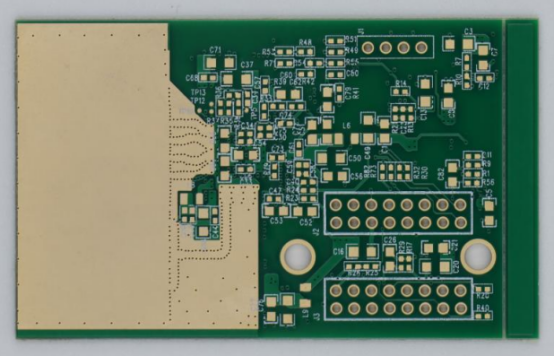
When we refer to an ultra-thin multilayer PCB, we are describing boards that are significantly thinner than standard multilayer PCBs, often with a total thickness of less than 0.4 mm. Despite their reduced thickness, these boards maintain multiple conductive layers, providing both density and functionality in a remarkably small form factor.
To better understand the difference, consider the three main PCB types:
Single-sided PCB: Features copper traces on only one side of the board, suitable for simple circuits.
Double-sided PCB: Has copper traces on both sides, allowing more complex circuits but still limited in layer count.
Multilayer PCB: Contains three or more layers, enabling high-density circuits in a compact space. When made ultra-thin, these boards are ideal for applications where weight, size, and flexibility are critical.
Manufacturing ultra-thin multilayer PCBs comes with unique challenges. One common issue is warpage, where the board bends or twists due to uneven thermal expansion during lamination. Another challenge is alignment precision; each internal layer must be perfectly registered to ensure vias connect correctly. Additionally, the lamination stress from compressing multiple thin layers can cause delamination or micro-cracks if not carefully controlled.
Despite these challenges, the benefits of ultra-thin multilayer PCBs—enabling miniaturization, higher component density, and lightweight electronics—make them a cornerstone of modern devices, from smartphones to 5G modules and advanced automotive systems.
Overview of Multilayer PCB Manufacturing Methods
Multilayer PCBs can be fabricated using different methods, each tailored to specific design requirements, density, and cost considerations. The two most common techniques are the Plated Through Hole (PTH) method and the High-Density Interconnect (HDI) additive process. Both methods enable multiple layers to connect electrically, but they differ in process, thickness control, and achievable circuit density.
Plated Through Hole (PTH) Method
The PTH method is the traditional and most widely used technique for fabricating multilayer PCBs. Developed over more than half a century, it has become highly mature, with well-established equipment, materials, and industrial standards.
This method is capable of producing double-sided and multilayer boards. Its core principle involves creating holes through the entire PCB stack, called vias, and then depositing a thin conductive layer on the walls of these holes. This metalization process electrically connects the inner layers with the outer layers, forming reliable interlayer connections.
Example: In a typical PTH process, a 6-layer PCB is drilled to create vias, chemically plated with copper to coat the hole walls, and then the entire board undergoes full-panel copper electroplating to ensure robust conductivity.
The PTH method is particularly well-suited for standard multilayer PCBs where layer count is moderate, and the design does not require extremely fine line spacing or ultra-thin structures. It is cost-effective and highly reliable due to its long history of industrial application.
High-Density Interconnect (HDI) Additive Process
The HDI additive process is a modern fabrication technique designed for very high-density multilayer PCBs. Instead of relying solely on through-holes, HDI boards use microvias, blind vias, and buried vias to connect layers. These vias are created using laser drilling or other precision additive methods, allowing for much finer circuit patterns and thinner board profiles.
Comparison with PTH method:
Thickness Control: HDI can achieve thinner overall board thickness than PTH, making it ideal for ultra-thin multilayer PCBs.
Circuit Density: HDI supports tighter spacing and more complex routing, enabling higher component density.
Cost: HDI boards are generally more expensive due to advanced materials, precision equipment, and complex processes.
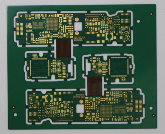
Example: A smartphone mainboard often uses HDI multilayer PCBs with up to 10+ layers and microvias, supporting ultra-fine pitch components that would be impossible with the traditional PTH method.
The PTH method is a mature, cost-effective solution for standard multilayer PCB fabrication, while the HDI process excels in high-density, ultra-thin designs where miniaturization and fine circuitry are essential. Choosing between the two depends on design complexity, thickness requirements, and budget constraints.
Step-by-Step Manufacturing Process of Ultra-Thin Multilayer PCBs
The production of ultra-thin multilayer PCBs involves a series of highly controlled steps, each critical to achieving reliability, precision, and performance in high-density circuits.
Step 1. Material Preparation and Cutting
The process begins with sourcing high-quality copper-clad laminates, prepreg, and copper foil. These materials serve as the core and insulating layers of the PCB. Standard board sizes from suppliers are typically large, such as 1m × 1m or 1m × 1.2m, and need to be cut to dimensions suitable for production lines.
Material cutting ensures that each panel fits the equipment while minimizing waste. Precise sizing is especially important for ultra-thin multilayer PCBs, as even minor deviations can affect layer alignment and final thickness.
Step 2. Inner Layer Circuit Fabrication
Once materials are prepared, the inner layer circuits are created. A photoresist or dry film is applied to the copper surfaces. The desired circuit patterns are then transferred using UV exposure through a film mask, followed by development to reveal the exposed copper.
Next, chemical etching removes unwanted copper, leaving only the defined traces. After etching, the photoresist is stripped, and the inner layers undergo AOI (Automated Optical Inspection) to detect defects such as broken traces or shorts.
Step 3. Brown Oxide Treatment
Before lamination, the inner layers undergo brown oxide treatment. This process roughens the copper surface and creates a thin oxide layer to:
1. Improve adhesion between copper and prepreg.
2. Enhance resin wetting into micro-cavities.
3. Prevent delamination or blistering during high-temperature lamination.
This treatment is crucial for ultra-thin boards, where layer adhesion is more sensitive to stress.
Step 4. Lamination Process
Lamination involves stacking the core, prepreg, and copper foil in the designed layer sequence. Heat and pressure are applied to bond the layers into a single solid board.
For ultra-thin multilayer PCBs, precise control of temperature, pressure, and duration is critical to prevent warping or uneven bonding. Improper lamination can lead to layer separation or inconsistent thickness.
Step 5. Drilling
After lamination, via holes are drilled using CNC machines or lasers. These holes connect the inner and outer layers electrically.
Maintaining high hole quality is essential; poorly drilled vias can cause delamination or poor electrical conductivity. Laser drilling is often preferred for microvias in high-density ultra-thin PCBs.
Step 6. Desmear, Chemical Copper Deposition, and Full-Panel Plating
Drilled holes often contain resin residues. Desmear removes these residues and roughens the hole walls. Next, chemical copper deposition deposits a thin copper layer on the hole walls, forming a conductive path.
Following this, full-panel electroplating increases copper thickness uniformly across the entire board. This differs from pattern plating, which selectively deposits copper only on exposed traces.
Step 7. Outer Layer Imaging and Pattern Plating
The outer layer circuits are formed using photoresist imaging similar to the inner layers. After exposure and development, pattern plating deposits copper and sometimes a thin tin layer on the exposed circuit paths to achieve the required thickness.
Step 8. Stripping and Etching
After pattern plating, the remaining photoresist is stripped, exposing unwanted copper. Chemical etching removes these areas, leaving only the precise outer layer circuitry.
Step 9. Solder Mask Application
The solder mask protects non-soldering areas from oxidation and prevents solder bridges during assembly. Green is the industry-standard color, but other colors are possible. The solder mask can be applied using screen printing, spray, or curtain coating.
Step 10. Silkscreen Printing
Next, silkscreen printing adds component designators, logos, and other markings onto the board surface. This aids assembly and inspection, improving manufacturing efficiency.
Step 11. Surface Finishing
Surface finishes protect exposed copper and improve solderability. Common options include ENIG (Electroless Nickel Immersion Gold), OSP (Organic Solderability Preservative), Immersion Tin, and HASL (Hot Air Solder Leveling). Selection depends on solderability, reliability, and cost requirements.
Step 12. Profile and Routing
The PCB is cut to its final shape using CNC routing, stamping, or manual cutting. CNC routing provides high precision, making it suitable for complex shapes, while manual cutting is limited to simple outlines.
Step 13. Testing and Final Inspection
Finally, the board undergoes electrical testing to check for open circuits and short circuits. Visual and functional inspections ensure that there are no cosmetic defects or layer misalignments. Only boards passing these tests are approved for shipment.
This structured process ensures that ultra-thin multilayer PCBs meet stringent requirements for high-density circuits, reliability, and miniaturization, supporting applications in smartphones, 5G modules, wearables, and advanced automotive electronics.
Key Challenges in Ultra-Thin Multilayer PCB Manufacturing
Manufacturing ultra-thin multilayer PCBs is a highly precise process that comes with several unique challenges. Each factor can affect the board’s performance, reliability, and yield, making careful control essential for high-quality production.
PCB Warpage and Thermal Stress
Warpage occurs when the PCB bends or twists during manufacturing, often caused by uneven thermal expansion of materials. In ultra-thin multilayer boards, the reduced thickness increases susceptibility to bending and distortion. Thermal stress during lamination, soldering, or surface finishing can further exacerbate warpage.
Example: A 0.3 mm thick 8-layer PCB may experience significant bowing if the lamination pressure or temperature is not evenly distributed. Excessive warpage can prevent proper component placement and lead to assembly failures.
Solution: Using low-Cu-content cores, balanced layer stackups, and precise thermal control during lamination helps minimize PCB warpage.
Alignment Tolerance Between Layers
Alignment tolerance refers to the precision with which internal layers are registered during lamination. Misalignment can cause vias to miss their target pads, creating open circuits or short circuits.
Example: In a 10-layer ultra-thin PCB with 4 mil line spacing, even a 2 mil misalignment can cause electrical failures.
Solution: Automated optical registration systems, careful handling, and precise lamination pressure are critical to maintain layer alignment tolerance within acceptable limits.
Copper Thickness Uniformity and Plating Control
Uniform copper thickness is essential for consistent electrical performance and reliability. Uneven copper deposition can lead to impedance variations, weak vias, and potential short circuits.
Example: During full-panel plating, if the current density is not carefully controlled, some areas may have thinner copper, reducing conductivity and long-term reliability.
Solution: Using controlled electroplating techniques, real-time monitoring, and regular measurement of copper thickness ensures consistency across the board.
Dimensional Stability and Reliability Testing
Ultra-thin multilayer PCBs are more prone to expansion or contraction under thermal or mechanical stress, affecting dimensional stability. This can lead to difficulties in assembly, especially for fine-pitch components.
Solution: Boards undergo reliability testing such as thermal cycling, humidity testing, and electrical testing to ensure they meet industry standards for durability and performance. These tests validate that the PCB can withstand real-world operating conditions without warping, delamination, or electrical failures.
The key challenges of ultra-thin multilayer PCB manufacturing—warpage, layer alignment, copper uniformity, and dimensional stability—require stringent process controls. Addressing these issues ensures high-density circuits function reliably in modern applications, from 5G devices to wearables and automotive electronics.
Applications of Ultra-Thin Multilayer PCBs
Ultra-thin multilayer PCBs are widely used across industries where compact size, high-density circuits, and reliable performance are critical. Their ability to integrate multiple layers in a small form factor makes them ideal for modern electronics.
Consumer Electronics
In consumer electronics, ultra-thin multilayer PCBs are essential for devices such as smartphones, tablets, and wearable devices. These products require boards that can support complex circuitry while remaining lightweight and slim.
Example: A modern smartphone mainboard may use an 8-layer or 10-layer ultra-thin PCB to accommodate high-speed processors, memory modules, and power management circuits without increasing device thickness. Similarly, smartwatches rely on ultra-thin PCBs to integrate sensors, wireless modules, and batteries in a small, curved housing.
Communication Equipment
5G network modules and other high-speed communication devices depend on ultra-thin multilayer PCBs for high-frequency signal transmission. Their compact size and precise layer alignment help maintain signal integrity and reduce interference in densely packed RF circuits.
Example: A 5G base station module may use an ultra-thin 12-layer HDI PCB to connect RF amplifiers, antennas, and control electronics while minimizing signal loss. The combination of fine-line traces and multiple layers ensures stable, high-speed data transmission.
Medical Electronics
In the medical electronics field, ultra-thin multilayer PCBs enable micro-monitoring devices, portable diagnostic tools, and implantable electronics. These applications require small, lightweight boards that can reliably operate in limited spaces without compromising performance.
Example: A wearable heart rate monitor or glucose sensor uses an ultra-thin multilayer PCB to integrate sensors, microcontrollers, and wireless communication modules, allowing continuous patient monitoring in a compact form.
Automotive Electronics
The automotive industry increasingly relies on ultra-thin multilayer PCBs in ADAS systems, in-car sensors, and infotainment modules. These boards must withstand high temperatures, vibrations, and other harsh environmental conditions while supporting advanced electronics.
Example: Advanced driver-assistance systems (ADAS) use multilayer HDI PCBs to process data from cameras, radar, and LiDAR sensors. Ultra-thin PCBs enable compact module designs that fit in tight spaces, reducing weight and improving vehicle efficiency.
Ultra-thin multilayer PCBs are crucial in applications requiring miniaturization, high reliability, and high-density circuitry. From consumer gadgets and 5G communication equipment to medical devices and automotive electronics, these boards play a central role in enabling the latest technological advancements.
Conclusion
Manufacturing ultra-thin multilayer PCBs is a precise and complex process, where each step—from material prep to final testing—affects performance and reliability.
Strict process control ensures layer alignment, copper uniformity, and lamination quality, preventing warpage, delamination, or electrical failures.
Partnering with experienced manufacturers like PCBMASTER guarantees high-quality boards for consumer electronics, 5G, medical devices, and automotive applications.
In short, careful multilayer PCB manufacturing is key to achieving reliable, high-performance electronics.
FAQs
Can ultra-thin multilayer PCBs handle high-frequency signals reliably?
Yes. Ultra-thin multilayer PCBs are designed with precise layer spacing and controlled impedance, which helps maintain signal integrity for high-frequency applications like 5G modules and advanced RF circuits. Proper material selection and plating techniques are critical for optimal performance.
What factors determine the maximum number of layers in an ultra-thin PCB?
The number of layers depends on board thickness, material properties, and manufacturing precision. Lamination stress, warpage risk, and drilling accuracy limit how many layers can be stacked without compromising reliability. Advanced HDI techniques can support more layers in thinner profiles.
How do manufacturers ensure long-term reliability of ultra-thin multilayer PCBs?
Manufacturers use a combination of thermal cycling, humidity testing, electrical testing, and visual inspections to verify durability. Careful control of lamination, plating, and solder mask application also ensures that boards maintain mechanical and electrical integrity over time.

