


Ultra HDI PCBs: Revolutionizing Electronics with Miniaturization and Speed
As electronic devices continue to shrink in size while becoming faster and more powerful, the demand for high-performance circuit boards has reached new heights. Ultra HDI (High-Density Interconnect) PCBs are leading this technological revolution, enabling the miniaturization of complex electronics without compromising performance.
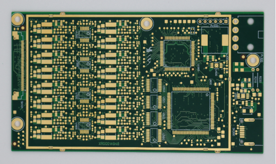
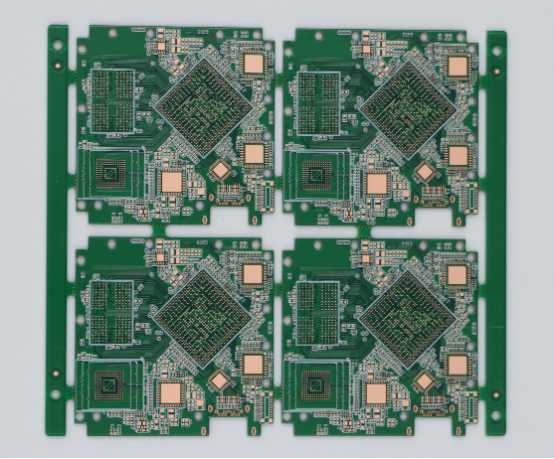
Ultra HDI (High-Density Interconnect) PCBs are advanced circuit boards designed to maximize the number of components and the performance of modern electronic devices. These boards are known for their ability to pack more components into a smaller space, offering high-speed connections and better signal integrity.
From the sleek smartphones in our pockets to life-saving medical implants, Ultra HDI is changing the way we design and build electronics. In this article, we’ll dive into the key advantages and features of Ultra HDI PCBs and explore how they’re helping to drive the future of innovation.
Key Advantages of Ultra HDI PCBs
Miniaturization and Space Efficiency
Ultra HDI PCBs are designed to be compact while providing high performance. This miniaturization allows devices to be smaller, lighter, and more efficient. Ultra HDI achieves this by using smaller microvias and finer traces (as thin as 25μm). These smaller components take up less space, enabling the integration of more parts in the same area.
Smaller Footprint and Thinner Profiles: Ultra HDI PCBs can reduce the size of devices by 30-50%. For example, a 5G module can be made much smaller without losing functionality. Similarly, wearables like health trackers or glucose monitors can be reduced to 25mm × 25mm in size, making them comfortable to wear on the skin while providing advanced features.
By using this space efficiently, Ultra HDI PCBs allow electronics to become more portable and sleek, which is crucial for wearable devices, smartphones, and other modern electronics.
Superior Signal Integrity (SI)
Signal integrity is critical for high-speed electronics like 5G or AI-driven devices. Ultra HDI PCBs are built to support high-frequency signals without losing data or causing interference.
Reduced Crosstalk and Low Signal Loss: Ultra HDI PCBs feature fine traces (25μm) and microvias, which help reduce signal loss and crosstalk. Crosstalk occurs when signals from one trace interfere with another, leading to performance issues. Ultra HDI minimizes this by using precise layouts and solid ground planes, ensuring clearer, faster data transmission.
Comparison of Signal Integrity at 28GHz vs Standard HDI PCBs: When testing signal performance at 28GHz, Ultra HDI PCBs maintain signal integrity much better than standard HDI PCBs. While standard HDI experiences 1.6dB loss per inch, Ultra HDI reduces this to 0.8dB, which results in better speed and reliability at high frequencies, crucial for applications like 5G communication and AI processing.
This enhanced signal integrity ensures that devices perform at their best, with minimal interference and data loss.
Enhanced Thermal Management
Efficient heat dissipation is essential for high-performance devices to prevent overheating and ensure long-term reliability. Ultra HDI PCBs are designed with advanced features to manage heat effectively.
Thick Copper Layers and Thermal Vias for Heat Dissipation: Ultra HDI PCBs use thicker copper layers (2–4oz) in the power and ground planes, which help spread heat more quickly, preventing hot spots. Additionally, thermal vias are used to transfer heat from components to other parts of the PCB, improving overall heat distribution. This prevents overheating, especially in high-power applications like 5G transmitters or autonomous vehicles.
Material Choices (e.g., Ceramic-filled substrates): To further enhance heat management, Ultra HDI PCBs often use ceramic-filled substrates, which have better thermal conductivity compared to traditional materials like FR4. This helps dissipate heat faster, making Ultra HDI suitable for power-hungry devices that generate a lot of heat, like smartphones and medical implants.
By effectively managing heat, Ultra HDI PCBs increase the lifespan of devices and improve their performance under heavy loads.
Improved Reliability
Ultra HDI PCBs are not only smaller and faster but also more reliable, especially in harsh conditions. Their robust construction makes them suitable for demanding environments where durability is essential.
Thermal Cycling and Vibration Resistance: Ultra HDI PCBs can withstand extreme temperature changes (from -40°C to 125°C) with a low failure rate of less than 1%. This makes them ideal for devices in automotive or aerospace applications, where they face constant temperature fluctuations and vibrations. They can handle 2,000 thermal cycles without breaking down, while standard HDI boards might fail after only 1,000 cycles.
Moisture Resistance and Long-Term Durability: Ultra HDI PCBs are designed to resist moisture absorption, which can lead to corrosion and failure over time. They use low-void prepreg and sequential lamination to ensure that the board stays dry and durable. This makes them perfect for devices that need to function in humid or high-moisture environments, such as wearable health monitors or medical implants.
With enhanced reliability, Ultra HDI PCBs provide long-lasting performance, even in the toughest conditions.
Key Features of Ultra HDI PCBs
Microvia Technology
Microvia technology is a core feature of Ultra HDI PCBs. It refers to tiny holes, known as microvias, that connect different layers of the PCB. These microvias help create compact, high-density designs essential for modern electronics.
Laser-Drilled Microvias: Sizes, Benefits, and Precision
Microvias are made using laser drilling, which provides high precision. They are typically as small as 45–75μm in diameter, much smaller than the holes used in traditional PCBs. Laser drilling ensures accurate placement and minimal damage to the surrounding materials. The benefit of smaller microvias is that they allow for more compact designs, enabling the integration of more components in a smaller space, essential for devices like smartphones and wearables.
Types of Microvias: Blind, Buried, and Stacked
There are different types of microvias, each serving specific purposes:
Blind Microvias: These connect the outer layer of the PCB to one or more inner layers. They are visible only from the outer side of the board.
Buried Microvias: These are located entirely inside the PCB and are not visible from the outer layers. They connect inner layers without passing through the outer layers.
Stacked Microvias: These involve two or more microvias stacked on top of each other, allowing for vertical connections between multiple layers. Stacked microvias enable higher density and more complex routing.
Each type of microvia helps improve the board’s compactness, signal integrity, and overall performance.
Fine-Line Traces
Ultra HDI PCBs use fine-line traces to route electrical signals between components. These traces are thinner than those found in traditional PCBs, making the board more compact and efficient.
25μm Trace Width and Spacing: Impact on Performance and Density
One of the defining features of Ultra HDI PCBs is the 25μm trace width and spacing. This refers to the narrow paths through which electrical signals travel. Traditional PCBs use thicker traces (around 50μm), but Ultra HDI uses finer traces to enable higher component density and better signal integrity. The reduced width and spacing allow for more components to fit in the same area without sacrificing performance. This is especially important for high-speed applications, such as 5G communication, where maintaining signal clarity and reducing interference are critical.
These fine traces ensure that Ultra HDI PCBs can handle complex designs while maintaining high-speed performance, making them ideal for advanced technologies like AI, IoT, and medical devices.
Layer Stacking and Sequential Lamination
Ultra HDI PCBs often require multiple layers to support complex designs, with layer stacking and sequential lamination being the main methods for creating these multi-layer boards. These processes ensure the board is both compact and highly functional.
Process Breakdown and Layer-to-Layer Alignment
Sequential lamination is the process of creating a PCB by building it in sub-layers or sub-stacks. Each sub-stack consists of a few layers that are laminated and aligned before the next set of layers is added. This process helps ensure precise layer-to-layer alignment, typically within ±3μm, which is crucial for the accuracy of stacked microvias. High precision in alignment ensures that the connections between the layers remain intact and that signals travel smoothly through the PCB without interference.
Importance for Complex Designs (e.g., 16-layer systems)
For complex designs like 16-layer systems, sequential lamination is essential. It allows for the creation of multi-layer PCBs without warping or misalignment. In devices that require many interconnections, such as advanced smartphones or medical implants, this technology makes it possible to build highly efficient, dense, and reliable circuit boards. The ability to stack layers precisely enables Ultra HDI PCBs to support complex circuits, increasing their functionality while keeping the size compact.
This approach is critical for the high-density, high-performance designs that modern electronics demand.
Performance Comparison: Ultra HDI vs. Traditional HDI & PCB Technologies
Component Density
Component density refers to how many components (such as resistors, capacitors, and integrated circuits) can fit onto a given area of a PCB. The higher the density, the more components can be packed into the same size board, which is crucial for modern, compact electronic devices.
Ultra HDI PCB: 1,800+ components per square inch
Ultra HDI PCBs offer an incredibly high component density of over 1,800 components per square inch. This is achieved through technologies like laser-drilled microvias and fine-line traces. The result is smaller, faster, and more powerful devices, such as 5G smartphones, wearable health monitors, and medical implants.
Traditional HDI: 900 components per square inch
In comparison, traditional HDI PCBs can accommodate only about 900 components per square inch. While this is still high-density compared to standard PCBs, it is less efficient than Ultra HDI. As a result, traditional HDI designs require more space and larger PCBs to house the same number of components.
The higher component density of Ultra HDI enables the creation of smaller devices with more functionality, making it ideal for compact, high-performance electronics.
Signal Loss at High Frequencies
At high frequencies, maintaining signal integrity is crucial for the performance of advanced electronic systems, especially in applications like 5G communication or AI processing.
Ultra HDI: <0.8dB/inch at 28GHz
Ultra HDI PCBs perform excellently in high-speed applications. For example, Ultra HDI PCBs experience less than 0.8dB loss per inch at 28GHz. This means that signals can travel longer distances through the board without losing quality, making it perfect for high-frequency devices like 5G modules and radar systems. Low signal loss ensures clearer data transmission, faster speeds, and higher reliability.
Traditional PCB: 3.0dB/inch at 28GHz
Traditional PCBs, on the other hand, experience higher signal loss—around 3.0dB per inch at the same 28GHz frequency. This higher loss leads to signal degradation, lower speeds, and increased interference, especially in high-frequency applications.
The low signal loss of Ultra HDI PCBs gives them a distinct advantage over traditional PCBs, particularly in high-speed and high-frequency applications where signal integrity is critical.
Size and Weight Reduction
Ultra HDI’s advanced manufacturing techniques also contribute to smaller and lighter boards, an essential factor in today’s miniaturized electronics.
Board Size Comparisons for Same Functionality
Ultra HDI PCBs can achieve the same functionality as traditional HDI or standard PCBs but in a significantly smaller form factor. For instance, an Ultra HDI-based 5G module can be made 30-50% smaller than a traditional HDI board, without losing any performance. This space-saving ability is crucial for devices that need to be compact, like smartphones, wearables, and medical implants.
In contrast, traditional HDI and regular PCBs take up more space to achieve the same performance, making them less ideal for modern devices that require small size and high functionality.
Ultra HDI's ability to shrink device size while maintaining full functionality is a game-changer for compact consumer electronics.
Thermal Cycling Survival
Thermal cycling refers to the ability of a PCB to survive temperature changes over time. This is particularly important in industries like automotive, aerospace, and medical devices, where devices face extreme temperature variations.
Ultra HDI’s Longer Lifespan vs. Standard HDI and Traditional PCBs
Ultra HDI PCBs are built to endure 2,000 thermal cycles between -40°C and 125°C, which means they can withstand extreme temperature fluctuations without failure. This robust thermal performance is a critical factor for devices used in harsh environments, like automotive electronics, and wearable devices.
In comparison, traditional HDI and standard PCBs typically survive only 1,000 cycles (for HDI) or 500 cycles (for standard PCBs), meaning they are more likely to fail when exposed to extreme or repeated temperature changes. The longer lifespan of Ultra HDI makes it a better option for long-lasting and high-reliability applications.
This superior thermal cycling performance ensures that Ultra HDI boards perform reliably in environments with wide temperature ranges, offering enhanced durability over time.
Conclusion
Ultra HDI PCBs offer a perfect blend of miniaturization, signal integrity, and reliability, making them ideal for applications like 5G, AI, and wearable health devices. With higher component density and faster signal transmission, they enable smaller, more efficient devices without sacrificing performance.
Looking ahead, Ultra HDI will be key to advancing technologies like 6G, AI, and compact medical devices, meeting the growing need for speed, size, and reliability.
In short, Ultra HDI is essential for next-gen electronics, offering unmatched performance for high-speed, high-density applications. At PCBMASTER, we specialize in providing high-quality Ultra HDI PCBs to bring your innovative ideas to life with precision and reliability.
FAQs
What are the key advantages of Ultra HDI PCBs over traditional HDI?
Ultra HDI PCBs offer several key advantages over traditional HDI, particularly in miniaturization, signal integrity, and improved thermal management. Ultra HDI boards are designed with smaller microvias and fine-line traces, which allow for higher component density and more compact designs. This leads to smaller, faster, and more efficient devices. Additionally, Ultra HDI ensures better signal integrity by reducing signal loss and crosstalk, especially at high frequencies. Improved thermal management is achieved through thicker copper layers, thermal vias, and high-conductivity materials, which efficiently dissipate heat, making Ultra HDI ideal for high-performance applications.
How does Ultra HDI handle high-frequency applications like 5G?
Ultra HDI is highly suited for high-frequency applications such as 5G. It supports high-speed signals up to 28GHz and beyond, ensuring low signal loss and minimal interference. This is achieved through precision microvias, fine-line traces, and controlled impedance to maintain signal integrity even at very high frequencies. As a result, Ultra HDI enables faster data transmission and reliable performance for advanced communication technologies like 5G.
Can Ultra HDI PCBs be used for flexible devices?
Yes, flexible Ultra HDI PCBs can be used in applications such as wearable devices and foldable phones. These flexible boards are made with polyimide substrates, which offer excellent flexibility and durability. The design allows them to bend and flex without damage, making them ideal for devices that require compact and flexible form factors.
What industries benefit most from Ultra HDI technology?
Ultra HDI technology benefits several key industries, including:
Telecommunications (for high-speed 5G and future 6G networks),
Medical devices (for miniaturized sensors and implants),
Automotive ADAS (for radar and LiDAR systems),
Aerospace (for advanced satellite communication systems),
Consumer electronics (for smaller, faster smartphones, wearables, and IoT devices).
These industries rely on Ultra HDI for its ability to deliver high-performance, miniaturized, and reliable circuit boards.
How does Ultra HDI improve the thermal performance of circuit boards?
Ultra HDI improves thermal performance by utilizing thick copper layers (2–4 oz), which spread heat more effectively than standard copper layers. Additionally, thermal vias are incorporated to transfer heat from high-power components to the inner layers of the board, keeping temperatures under control. High-conductivity materials, such as ceramic-filled substrates, further enhance heat dissipation, ensuring that Ultra HDI PCBs maintain optimal performance even in high-power applications.

