The Ultimate Guide to PCBA Manufacturing: Processes, Tips, and Best Practices
In today’s fast-paced electronics industry, the quality and reliability of a device often hinge on its Printed Circuit Board Assembly (PCBA). From smartphones to industrial machinery and IoT devices, every product relies on these intricate boards to function flawlessly. Yet behind the sleek designs and powerful features lies a complex process that determines performance, durability, and efficiency. Understanding how PCBA manufacturing works—and how to optimize it—can make the difference between a product that excels and one that falls short.
Introduction to PCBA Manufacturing
What is PCBA Manufacturing?
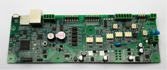
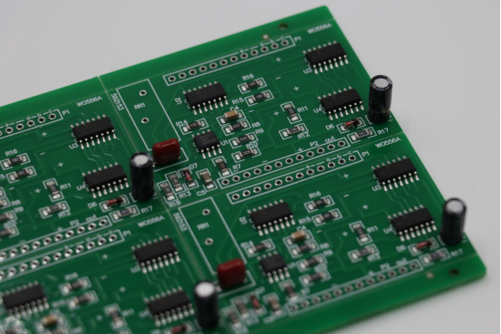
Printed Circuit Board Assembly (PCBA) manufacturing is the process of attaching electronic components onto a printed circuit board (PCB) to create a fully functional electronic assembly. Unlike a bare PCB, which is simply the board with etched circuits, PCBA combines the board with all required components—resistors, capacitors, integrated circuits, connectors, and more—through precise soldering and assembly processes.
The key difference between PCB and PCBA lies in functionality: a PCB alone is passive and cannot perform any electronic operation. Once components are assembled, it becomes a PCBA capable of powering devices, processing signals, or communicating with other systems. For example, a bare PCB might contain the printed copper traces for a smartphone motherboard, but only after assembly with chips, connectors, and other components does it become the working motherboard.
PCBA manufacturing is critical in modern electronics because it enables the miniaturization, reliability, and high performance required in today’s devices. From smartphones to wearable devices and industrial control systems, almost every electronic product depends on precise and high-quality PCBA to function correctly. Without proper assembly processes, even the most sophisticated PCB designs cannot achieve the desired performance or longevity.
Key Benefits of High-Quality PCBA
Reliability and performance improvements are among the most significant advantages of well-executed PCBA manufacturing. High-quality assembly ensures that all components are properly placed, soldered, and electrically connected, reducing the risk of failures caused by poor connections, short circuits, or component misalignment. For instance, automotive electronics require strict reliability because a single failure could compromise safety.
Cost efficiency and scalability are additional benefits. Accurate assembly reduces waste from defective boards and minimizes rework costs. Standardized processes allow manufacturers to scale production efficiently while maintaining quality. For example, IoT device producers can mass-produce boards with consistent quality across hundreds of thousands of units, keeping production costs under control.
Real-world examples highlight the impact of high-quality PCBA. Smartphones rely on densely packed boards with multiple layers and tiny components; even a small assembly error can affect signal integrity or battery life. Industrial IoT devices need robust PCBA capable of withstanding harsh environments while maintaining connectivity and performance. In both cases, proper PCBA manufacturing ensures the final product meets reliability, durability, and functional expectations.
PCBA Manufacturing Processes
PCB Fabrication vs. PCB Assembly
PCB fabrication is the process of creating the bare circuit board before components are added. Key steps include:
Design and layout: Engineers define the circuit paths and layer stack-up.
Material preparation: Substrates like FR4 or high-frequency laminates are cut to size.
Etching and copper plating: Copper traces are formed to connect components.
Drilling and plating through-holes: Holes for components or vias are created and plated for electrical connectivity.
Solder mask and silkscreen application: Protective coatings and markings are added for assembly guidance.
Transitioning to PCB assembly involves taking the fabricated board and attaching all electronic components to form a fully functional PCBA. The assembly process includes solder paste application, component placement, soldering, and inspection.
Comparison:
Fabrication only: Produces a bare PCB, useful for prototyping or design verification but not functional by itself.
Complete assembly (PCBA): Adds all necessary components, making the board operational and ready for deployment in devices.
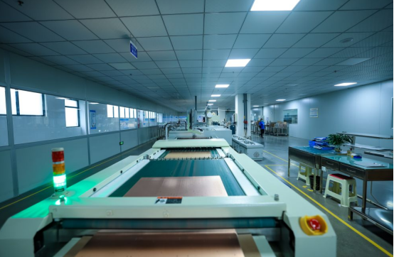
Surface Mount Technology (SMT)
SMT is the most widely used PCBA process for modern electronics. It involves mounting components directly onto the surface of the PCB.
Step-by-step SMT process:
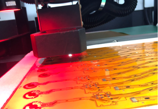
1. Solder paste application: A stencil deposits solder paste onto PCB pads.
2. Pick-and-place: Automated machines place surface-mount components accurately onto the solder paste.
3. Reflow soldering: The board passes through a reflow oven where heat melts the solder, forming strong electrical connections.
Common components used in SMT:
Resistors, capacitors, diodes
Integrated circuits (ICs), microcontrollers
LEDs, sensors
Example: High-volume smartphone PCBA uses SMT for millions of tiny components, allowing fast production with high precision and minimal human intervention.
Through-Hole Technology (THT)
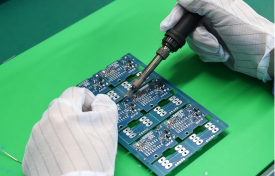
THT involves inserting component leads through pre-drilled holes in the PCB and soldering them on the opposite side.
Step-by-step THT process:
1. Components are inserted manually or by automated machines.
2. The board goes through wave soldering or hand soldering to secure connections.
3. Final trimming ensures proper fit and safety.
Comparison with SMT:
Durability: THT provides stronger mechanical bonds, ideal for connectors or high-stress components.
Application: Common in industrial machinery, automotive electronics, or boards requiring robust mechanical support.
Example: Industrial machinery PCBA often uses THT for power connectors and heavy-duty components to ensure long-term reliability.
Mixed Technology Assembly
Mixed technology combines SMT and THT on the same board to leverage the advantages of both.
Best practices for hybrid assemblies:
Prioritize SMT placement first, followed by THT insertion.
Optimize reflow and wave soldering profiles to prevent component damage.
Use automated inspection tools to verify both SMT and THT connections.
This approach is common in high-performance or industrial boards that need both fine-pitch ICs and strong mechanical connectors.
Inspection and Quality Control
Quality control ensures that PCBAs are reliable and defect-free.
In-process inspection:
Automated Optical Inspection (AOI): Detects missing or misaligned components.
Solder Paste Inspection (SPI): Verifies correct paste volume and placement.
Final inspection:
X-ray inspection: Checks hidden solder joints, such as BGA (Ball Grid Array) components.
Functional testing: Verifies board operation under real-world conditions.
Step-by-step defect detection workflow:
1. Inspect solder paste deposition.
2. Verify component placement post pick-and-place.
3. Inspect solder joints after reflow or wave soldering.
4. Conduct functional testing and address failures with rework.
This structured approach ensures that every PCBA meets performance, reliability, and safety standards.
Materials and Components in PCBA
PCB Substrates and Core Materials
The PCB substrate is the foundational material that supports circuits and components. Common types include:
FR4: A widely used, cost-effective fiberglass epoxy laminate suitable for most standard electronics.
Rogers: A high-frequency laminate ideal for RF and microwave applications due to low dielectric loss.
High-frequency materials: Specialized substrates for advanced telecommunications, 5G, and high-speed digital circuits.
Selection criteria for PCB substrates include:
Electrical performance: Dielectric constant (Dk) and dissipation factor (Df) affect signal integrity.
Thermal stability: Materials must withstand assembly and operational temperatures.
Mechanical strength: Supports heavy or high-density components.
Cost considerations: High-performance substrates are more expensive but necessary for advanced applications.
Example: A high-speed communication board may use Rogers or a low-Dk material to reduce signal loss, whereas a standard consumer device can use FR4 to balance cost and performance.
Electronic Components
PCBA relies on both passive and active components:
Passive components: Resistors, capacitors, and inductors that do not require power to operate.
Active components: ICs, transistors, diodes, and microcontrollers that require power and perform functions such as amplification or computation.
Sourcing considerations for reliability:
Choose certified suppliers with proven quality standards.
Verify component lifespan and environmental ratings (temperature, humidity).
Ensure availability to prevent supply chain disruptions.
Example: Automotive PCBA may require capacitors rated for wide temperature ranges and ICs with automotive-grade certifications to ensure long-term reliability.
Solder and Flux Types
Solder and flux are essential for creating strong electrical and mechanical connections.
Leaded vs. lead-free solder:
Leaded solder (SnPb): Offers lower melting points and easier processing but is restricted in many regions due to environmental regulations.
Lead-free solder (SnAgCu, SAC alloys): Environmentally compliant, slightly higher melting point, requires precise process control.
Flux types and their roles:
Rosin-based flux: Cleans surfaces and promotes wetting.
No-clean flux: Leaves minimal residue, reducing post-process cleaning.
Water-soluble flux: Easily removable, suitable for sensitive applications.
Example: For high-temperature PCBA applications, such as industrial motor controllers, SAC305 lead-free solder with rosin-based flux may be chosen to ensure strong connections without component damage during reflow.
Design Considerations for Efficient PCBA Manufacturing
Design for Manufacturability (DFM)
Design for Manufacturability (DFM) focuses on creating PCB designs that are easy and cost-effective to manufacture while minimizing assembly errors. Key guidelines include:
Trace width and spacing: Ensure traces are wide enough to handle current and avoid short circuits, while keeping spacing sufficient to prevent solder bridging.
Component placement: Avoid placing components too close together, especially those requiring hand soldering or thermal management.
Standardized footprints: Use widely accepted component sizes to simplify sourcing and assembly.
Minimize complex vias and blind/buried holes: Reduces drilling errors and lowers manufacturing cost.
Example: On a high-density board, increasing trace width from 4 mils to 6 mils for power traces can improve yield and reduce solder defects without significantly increasing board size.
Design for Testability (DFT)
Design for Testability (DFT) ensures that boards can be easily tested and troubleshooted during production and maintenance.
Key strategies:
Test points: Include accessible pads for voltage, signal, and current testing.
Modular layout: Group functional blocks together for easier isolation of faults.
Built-in self-test (BIST): Integrate circuits that allow automated diagnostics.
Step-by-step approach to ensure testability:
1. Identify critical signals and power lines for monitoring.
2. Place test points at accessible locations without interfering with components.
3. Design modular circuits to allow partial board testing.
4. Validate DFT features during prototype testing to detect potential issues early.
Example: An industrial IoT board might include dedicated voltage test points for each power rail to quickly identify faults during assembly or field maintenance.
Signal Integrity and High-Speed Design
High-frequency or high-speed boards require careful design to maintain signal integrity, avoiding signal loss, reflections, and crosstalk.
Importance: Poor signal integrity can lead to communication errors, data loss, or device malfunction in applications like 5G, high-speed data converters, or advanced processors.
Techniques for reliable high-speed PCBA design:
Controlled impedance traces: Maintain consistent trace width, spacing, and dielectric properties for predictable signal behavior.
Layer stacking: Use ground and power planes to reduce noise and improve return paths.
Differential pair routing: Ensures balanced high-speed signals with minimal interference.
Comparison of good vs. poor layout impact:
Good layout: Clean signal paths, minimal reflections, predictable timing, and reduced EMI.
Poor layout: Increased crosstalk, signal degradation, and higher failure rates in functional testing.
Example: On a high-speed networking board, using proper differential pair routing and controlled impedance can reduce bit error rates from 10^-9 to below 10^-12, improving overall reliability.
Best Practices in PCBA Manufacturing
Process Optimization
Optimizing PCBA manufacturing processes improves efficiency, reduces errors, and lowers production costs.
Lean manufacturing principles are widely applied:
Eliminate waste: Reduce excess material usage, minimize rework, and streamline workflows.
Standardize processes: Consistent procedures improve repeatability and yield.
Continuous improvement (Kaizen): Regularly assess and refine processes to identify bottlenecks or quality issues.
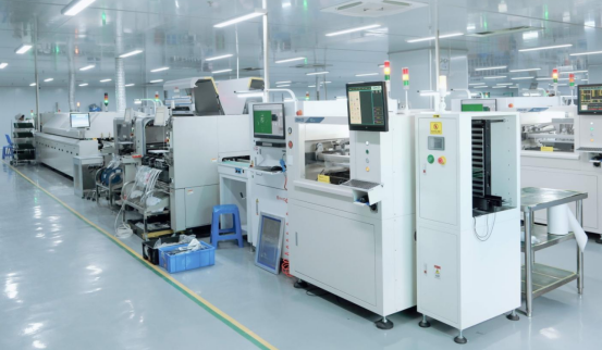
Automated assembly vs. manual assembly:
Automated assembly: High-speed pick-and-place machines, reflow ovens, and automated inspection reduce human error and increase throughput, ideal for high-volume production.
Manual assembly: Necessary for complex, low-volume, or specialized boards, but slower and prone to inconsistency.
Example: A consumer electronics manufacturer may use automated SMT assembly for thousands of smartphone boards per day, while manual assembly is reserved for prototypes or boards with irregular component layouts.
Quality Assurance
High-quality PCBA requires rigorous quality assurance (QA) practices.
Implementing ISO and IPC standards:
ISO 9001: Ensures consistent quality management systems.
IPC-A-610: Defines acceptability standards for electronic assemblies, including soldering quality, component placement, and cleanliness.
Continuous process monitoring:
Track production metrics such as defect rates, solder joint quality, and rework instances.
Use automated inspection systems (AOI, X-ray) to detect issues early.
Maintain detailed records for traceability and corrective actions.
Example: In an automotive PCBA line, continuous monitoring can identify soldering issues immediately, preventing faulty boards from reaching safety-critical systems.
Supplier and Component Management
Reliable components and suppliers are critical to PCBA success.
Vetting component suppliers:
Evaluate suppliers for certifications, quality history, and delivery performance.
Conduct audits to ensure compliance with specifications.
Inventory and lifecycle management:
Monitor component availability to prevent production delays.
Plan for obsolescence and phase out components in a controlled manner.
Example: A medical device manufacturer may maintain multiple vetted suppliers for critical ICs to ensure uninterrupted production and regulatory compliance.
Environmental and Regulatory Compliance
Adhering to environmental and regulatory standards ensures legal compliance and sustainability.
RoHS and REACH compliance:
RoHS: Restricts hazardous substances like lead, mercury, and cadmium in PCBs.
REACH: Regulates chemicals used in electronic manufacturing to minimize environmental and health impacts.
E-waste management and sustainability:
Implement recycling programs for defective boards and leftover materials.
Use energy-efficient equipment and reduce material waste.
Example: A consumer electronics company might recycle scrap PCBs and enforce lead-free solder processes to meet RoHS standards while minimizing environmental impact.
Common Challenges and How to Overcome Them
Soldering Defects
Soldering defects are one of the most common issues in PCBA manufacturing.
Types of soldering defects:
Cold solder joints: Occur when solder fails to melt completely, resulting in weak or intermittent connections.
Bridging: Excess solder creates unintended connections between adjacent pads or leads.
Tombstoning: Small components lift on one side during reflow, resembling a tombstone.
Step-by-step corrective actions:
Cold solder: Reflow the affected joint with proper temperature profiling.
Bridging: Remove excess solder using solder wick or hot air rework and inspect with AOI.
Tombstoning: Adjust component placement, solder paste volume, and reflow profile to ensure even melting.
Example: On a high-density smartphone PCBA, tombstoning of 0402 resistors can be prevented by controlling solder paste deposition and using precise pick-and-place machines.
Component Misalignment
Causes:
Inaccurate pick-and-place machine calibration
Uneven solder paste application
Mechanical vibration during reflow
Prevention methods:
Regular machine calibration and maintenance
Optimized stencil design for consistent solder paste volume
Proper board handling and fixturing during reflow
Example: For automotive PCBA, aligning connectors precisely prevents stress on solder joints and ensures reliable mechanical and electrical connections under vibration.
Thermal Management Issues
High-power components or dense PCBA layouts can generate hot spots, leading to failure or reduced lifespan.
Identifying hot spots:
Thermal imaging cameras during functional testing
Simulation software during design phase
Cooling techniques and material choices:
Heat sinks and thermal vias: Transfer heat away from critical components.
High thermal conductivity substrates: Improve heat dissipation.
Active cooling: Fans or liquid cooling in high-power boards.
Example: An industrial motor controller PCBA uses thermal vias and heat sinks to manage the temperature of MOSFETs, ensuring stable operation under high load.
Supply Chain Disruptions
Component shortages or delays can significantly impact production timelines.
Contingency planning:
Maintain safety stock for critical components
Implement flexible production schedules to accommodate delays
Alternative sourcing strategies:
Vet multiple suppliers for essential components
Use interchangeable or equivalent parts where possible
Example: A medical device manufacturer may source ICs from multiple certified suppliers to avoid production halts due to a single-source disruption.
Future Trends in PCBA Manufacturing
Automation and Smart Factories
Automation and smart manufacturing are transforming PCBA production lines. AI and robotics enable faster, more precise assembly while reducing human error.
Key applications:
Vision-guided pick-and-place: Robotic arms equipped with cameras identify component positions and orientation, ensuring accurate placement even for ultra-fine pitch components.
Automated inspection: AI-driven AOI and X-ray systems detect defects in real-time, reducing rework and improving yield.
Example: A high-volume smartphone PCBA line may use vision-guided robots to place tens of thousands of tiny components per hour with sub-millimeter accuracy, significantly improving throughput and reliability.
Advanced Materials
Emerging materials are shaping the next generation of PCBAs.
Flexible PCBs: Allow bending or folding, enabling compact designs for wearables, foldable devices, and medical implants.
High-speed laminates: Low-dielectric-loss materials like Rogers or PTFE substrates support high-frequency circuits, critical for 5G, radar, and high-speed data applications.
Example: A 5G communication module may use high-speed laminates combined with a flexible PCB section to connect antennas without signal degradation.
Industry 4.0 and Data Analytics
Industry 4.0 integrates connected systems and data analytics into PCBA manufacturing for smarter operations.
Real-time monitoring: Sensors track temperature, humidity, soldering profiles, and machine performance across the production line.
Predictive maintenance: AI analyzes data trends to forecast equipment failure, allowing preventive interventions before downtime occurs.
Example: In a large automotive PCBA plant, predictive maintenance reduces unexpected reflow oven failures, ensuring consistent production while minimizing waste and delays.
Conclusion
High-quality PCBA manufacturing relies on a careful balance of design, process, and quality control. From selecting the right substrates and components to optimizing assembly processes and ensuring signal integrity, every step contributes to reliable, high-performance boards.
Adopting best practices—including Design for Manufacturability (DFM), Design for Testability (DFT), rigorous quality assurance, and advanced inspection—reduces defects, improves efficiency, and ensures that your products meet both technical and regulatory standards.
PCBMASTER, as an experienced PCB and PCBA supplier, can provide expert guidance, process consultation, and tailored solutions to help you achieve optimal assembly performance. Leveraging professional support ensures that your PCBA projects are not only functional but also scalable, cost-effective, and reliable.
FAQs
Question | Answer | Key Example / Notes |
|---|---|---|
What is the difference between PCB fabrication and PCBA assembly? | PCB fabrication creates the bare circuit board (etching, drilling, plating, solder mask) and is not functional. PCBA assembly adds electronic components (SMT/THT) to make the board operational. | Fabrication = board only; Assembly = fully functional PCB. |
How does SMT compare to THT in terms of durability and cost? | SMT mounts components on the surface; cost-effective, suitable for mass production, smaller components. THT inserts leads through holes; more durable mechanically but slower and more expensive. | SMT: smartphones; THT: industrial boards. |
What are the most common defects in PCBA manufacturing and how can they be prevented? | Common defects: cold solder joints, solder bridging, tombstoning, component misalignment. Prevention: proper solder paste, temperature profiling, pick-and-place calibration, AOI/X-ray inspection, functional testing. | Tombstoning prevention: control solder volume and reflow profile. |
How do you choose the right materials for high-frequency PCBAs? | Consider low Dk and Df for minimal signal loss, thermal stability, and mechanical strength. Use high-frequency materials like Rogers or PTFE laminates. | Example: 5G communication boards use Rogers for signal integrity. |
What role does automation play in modern PCBA manufacturing? | Automation ensures speed, accuracy, and consistency. Applications: pick-and-place, reflow ovens, vision-guided systems, AI-driven AOI/X-ray inspection. Benefits: higher throughput, lower defects, scalable production. | Example: Vision-guided robots in smartphone PCBA lines. |