


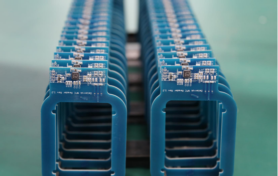
A Complete Guide to Printed Circuit Board Supplies: Materials, Tools, and Components
Printed circuit boards (PCBs) are the silent foundation of modern electronics, enabling compact, high-speed, and reliable connections in everything from consumer gadgets to advanced communication systems. The performance of a PCB, however, is not defined by design alone—it’s shaped by the quality of the materials, tools, and components used in its creation.
From the choice of base laminates to the precision of drilling and the reliability of surface finishes, every element contributes to the electrical stability and long-term durability of the final board. Understanding how these supplies work together is key to achieving consistent performance and manufacturing efficiency in any PCB production process.
Introduction to Printed Circuit Board Supplies
What Are PCB Supplies?
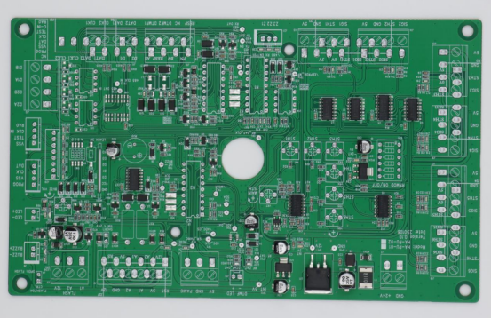
Printed circuit board (PCB) supplies refer to all the materials, tools, and accessories required to fabricate and assemble a PCB. These include laminates, copper foils, prepregs, solder masks, surface finishes, drilling and etching equipment, and assembly tools such as pick-and-place machines or reflow ovens. Together, they form the physical and operational foundation that allows circuits to function reliably in electronic devices.
The selection of PCB supplies directly influences quality, reliability, and electrical performance. For example, choosing a high-frequency laminate with a low dielectric loss (Df) helps maintain signal integrity in 5G and high-speed data systems. Similarly, precision drilling tools reduce the risk of via misalignment, ensuring consistent electrical connectivity across multilayer designs.
In simple terms, PCB supplies determine how well a board performs under electrical, thermal, and mechanical stress. Using the right combination of materials and equipment results in stable impedance, smooth signal transmission, and a longer service life for the finished product.
Why Choosing the Right Supplies Matters
Selecting the proper PCB supplies is not just about meeting design requirements—it’s about optimizing the entire manufacturing ecosystem. High-quality materials and tools enhance signal integrity, improve yield rates, and reduce manufacturing costs over time. For instance, a consistent laminate thickness minimizes impedance variations, while accurate solder paste application during assembly reduces rework and scrap.
In contrast, low-cost or substandard supplies often lead to hidden expenses. Poor-quality copper foil may cause uneven plating or delamination, while cheaper solder masks can degrade under heat, increasing the risk of short circuits or corrosion. These issues not only affect performance but can also raise production costs through increased inspection time, rework, and warranty claims.
A practical way to evaluate supply quality is by considering lifecycle performance rather than initial cost. While premium materials like Rogers 4350B or MEGTRON 6 come at a higher price, their superior signal stability and thermal endurance often translate into lower total cost of ownership for high-speed or mission-critical applications.
Ultimately, the right PCB supplies help manufacturers achieve consistent performance, reduce failure rates, and maintain competitiveness in demanding markets such as telecommunications, automotive, and aerospace electronics.
Essential PCB Materials
Base Laminates and Substrates
Base laminates and substrates form the structural and electrical foundation of every printed circuit board. They determine the board’s mechanical strength, dielectric behavior, and thermal stability. Common materials include FR-4, Rogers, Polyimide, PTFE, and Metal-core laminates, each offering unique performance characteristics.
Material Type | Dielectric Constant (Dk) | Loss Tangent (Df @10GHz) | Heat Resistance | Key Features / Applications |
|---|---|---|---|---|
FR-4 | ~4.3 | 0.02 | 130–140°C | Standard multilayer PCBs; cost-effective and reliable. |
Rogers (e.g., 4350B) | 3.48 | 0.0037 | 200°C+ | High-frequency and RF designs requiring low signal loss. |
Polyimide | 3.5–4.0 | 0.004–0.01 | 250°C+ | Flexible and high-temperature applications such as aerospace. |
PTFE (Teflon) | 2.1 | 0.0009 | 260°C+ | Microwave and high-speed communication circuits. |
Metal-Core (MCPCB) | Varies | N/A | Excellent thermal conduction | LED lighting, power electronics, and heat-dissipating boards. |
Use Cases:
High-frequency boards use low-Dk, low-Df laminates such as Rogers or PTFE for stable impedance and reduced signal loss.
Flexible PCBs rely on polyimide substrates for bendability and thermal endurance.
High-power designs often use metal-core laminates to efficiently dissipate heat away from power components.
Copper Foil Types
Copper foil serves as the conductive layer of the PCB, forming traces and vias that carry electrical signals. There are two main types: Electrodeposited (ED) and Rolled Annealed (RA) copper.
Electrodeposited (ED) copper is produced by electroplating copper onto a rotating drum. It has a rougher surface and is ideal for rigid PCBs, offering good adhesion to the substrate.
Rolled Annealed (RA) copper is made by mechanically rolling and heat-treating copper, resulting in a smoother surface and higher ductility. It’s preferred for flex and flex-rigid PCBs due to its excellent bend performance.
Copper Thickness and Its Effects:
Thicker copper (e.g., 2 oz/ft²) increases current-carrying capacity and thermal dissipation, essential for power circuits.
Thinner copper (e.g., 0.5 oz/ft²) provides better signal integrity for high-frequency designs by minimizing impedance variations.
A balance is key: choosing the right thickness prevents overheating without compromising fine trace resolution.
Prepregs and Bonding Sheets
Prepregs are partially cured fiberglass sheets impregnated with resin, used to bond copper-clad cores during multilayer PCB lamination. Bonding sheets serve a similar role but may have different resin systems for specific mechanical or dielectric needs.
Step-by-Step: How Prepreg Bonding Works
1. Layer Stacking: Alternating layers of copper-clad cores and prepregs are aligned according to the circuit design.
2. Pressing and Heating: The stack is placed in a lamination press under controlled temperature and pressure.
3. Resin Flow: Heat softens the resin in the prepreg, allowing it to flow and fill microscopic gaps between layers.
4. Curing: The resin hardens, permanently bonding the layers into a single multilayer PCB with stable dielectric spacing.
Accurate prepreg selection ensures consistent dielectric thickness, prevents delamination, and maintains the board’s electrical insulation properties.
Solder Mask and Silkscreen Materials
Solder masks protect copper circuits from oxidation, solder bridging, and mechanical wear. Common types include epoxy liquid, dry film, and LPI (Liquid Photoimageable) solder masks.
Epoxy liquid: Economical and durable but limited in precision.
Dry film: Offers high accuracy but less suited for complex geometries.
LPI: The industry standard, allowing precise definition for fine-pitch components.
Comparison Factors:
Chemical resistance: LPI provides superior resistance to flux and cleaning agents.
Resolution: Dry film and LPI offer better fine-line coverage than epoxy.
Color impact: Green is most common due to optimal visibility during inspection; other colors like black or white may affect optical AOI detection accuracy.
Silkscreen materials (usually epoxy-based inks) are used for labeling and component identification, ensuring readability through assembly and maintenance.
Surface Finishes
Surface finishes protect exposed copper pads and enhance solderability during assembly. Common finishes include ENIG, HASL, OSP, and Immersion Tin/Silver.
ENIG (Electroless Nickel Immersion Gold): Provides excellent flatness and corrosion resistance; ideal for fine-pitch and BGA components.
HASL (Hot Air Solder Leveling): Cost-effective and durable but less suitable for high-density layouts.
OSP (Organic Solderability Preservative): Simple and environmentally friendly, used for short production cycles.
Immersion Tin/Silver: Offer flat surfaces and good solderability, though with limited shelf life compared to ENIG.
ENIG vs. HASL Example:
ENIG: Superior for fine-pitch SMDs due to smooth surface and oxidation resistance.
HASL: Better for through-hole assemblies and budget-sensitive production.
Key Selection Factors:
Shelf life: ENIG > Immersion Silver > HASL > OSP.
Solderability: ENIG and HASL perform best under multiple reflow cycles.
Cost: OSP and HASL are lower-cost alternatives for standard applications.
In summary, selecting the right combination of base laminates, copper foils, prepregs, solder masks, and surface finishes ensures stable electrical performance, structural reliability, and cost efficiency throughout the PCB manufacturing process.
Essential Tools and Equipment
Fabrication Tools
PCB fabrication begins with mechanical and laser processes that define the board’s physical structure. The most critical tools include drilling machines, CNC routers, and laser drills.
Drilling machines create vias and through-holes that connect different PCB layers.
CNC routers shape the PCB outline and separate individual boards from production panels.
Laser drills deliver extreme precision for microvias used in HDI (High-Density Interconnect) designs.
Step-by-Step: How Drilling Precision Is Achieved
1. Tool Selection: Choose the correct drill bit diameter and type (mechanical or laser) based on hole size and board thickness.
2. Registration and Alignment: Optical systems align drill coordinates to ensure positional accuracy within microns.
3. Drilling Execution: Controlled spindle speed and feed rate minimize burrs and prevent delamination.
4. Aspect Ratio Evaluation: The aspect ratio (board thickness ÷ hole diameter) is checked—ratios above 10:1 can affect plating uniformity and reliability.
Precise drilling ensures electrical connectivity between layers and directly influences via integrity, signal continuity, and yield rates.
Etching and Plating Equipment
Etching and plating are essential processes that form conductive traces and protective coatings on a PCB.
Chemical etching uses acid-based solutions to remove unwanted copper, creating circuit patterns.
Plasma etching employs ionized gas for precise removal, ideal for fine-line and HDI boards.
Plating Equipment and Thickness Control:
Plating deposits copper or other metals (nickel, gold, tin) onto surfaces and vias. Controlling plating thickness ensures uniform conductivity and via reliability:
Under-plating may cause open circuits or weak interlayer connections.
Over-plating can distort fine traces or cause shorts between vias.
Typical copper plating thickness ranges from 20–25 μm for through-holes, while surface finishes like ENIG or HASL add thin protective layers that support solderability during assembly.
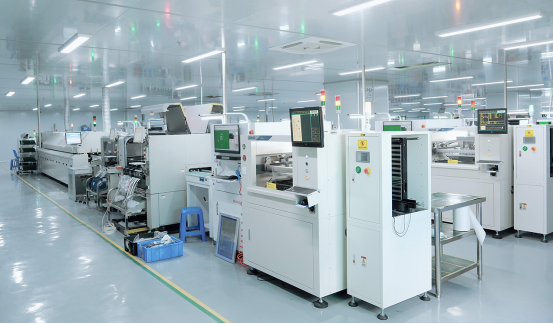
Assembly Tools
After fabrication, PCBs move into the assembly stage, where electronic components are mounted onto the board. The main assembly tools are pick-and-place machines, reflow ovens, and stencil printers.
Pick-and-place machines automatically position SMD (Surface Mount Device) components with micron-level accuracy.
Stencil printers apply solder paste evenly across pads, defining the quality of solder joints.
Reflow ovens melt the solder paste under a controlled temperature profile to form solid electrical connections.
Example: How Accurate Placement Impacts SMT Yield
When components are precisely placed, solder joints form evenly, preventing defects like bridging or tombstoning. Even a ±50 µm misalignment can reduce yield by 10–20% in dense BGA assemblies. High-precision vision systems in modern pick-and-place machines correct such deviations in real time, ensuring consistent production quality.
Inspection and Testing Tools
To verify functionality and detect defects, PCB manufacturers use inspection and testing tools throughout production. Common systems include AOI (Automated Optical Inspection), flying probe testers, and X-ray inspection.
AOI systems use high-resolution cameras to detect issues such as missing components, solder bridges, or trace breaks.
Flying probe testers check electrical continuity and isolation without the need for custom test fixtures—ideal for prototypes or small batches.
X-ray inspection penetrates layers to analyze hidden solder joints under BGAs or multilayer vias.
Comparison of Testing Methods:
Method | Primary Detection Target | Best For | Advantages | Limitations |
|---|---|---|---|---|
AOI | Visual defects (misalignment, shorts) | SMT and reflow inspection | Fast, non-contact | Limited to surface defects |
Flying Probe | Opens, shorts, component values | Prototyping, low-volume | No fixture required | Slower for mass production |
X-ray | Hidden solder joints, internal vias | Complex multilayer PCBs | Reveals internal defects | High cost, skilled operation required |
Together, these inspection systems ensure that every PCB meets electrical and mechanical specifications before delivery, reducing field failures and improving long-term reliability.
In summary, fabrication and assembly tools form the backbone of PCB production. Accurate drilling, precise etching, controlled plating, and thorough inspection work together to produce boards that meet the demanding standards of modern electronics manufacturing.
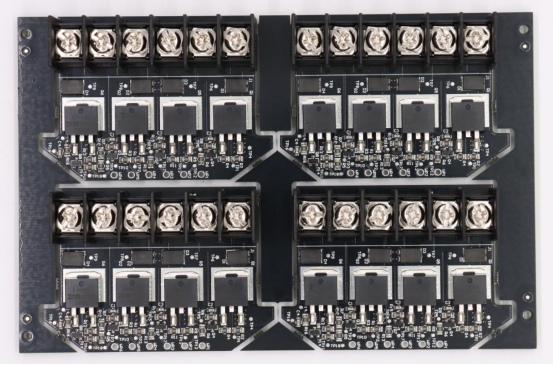
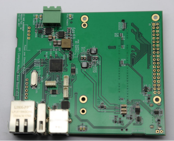
PCB Components and Accessories
Common Components Used in PCB Assembly
Every printed circuit board functions through a combination of electronic components mounted on its surface or embedded within its layers. The most common components used in PCB assembly include resistors, capacitors, inductors, integrated circuits (ICs), and connectors.
Resistors control current flow and voltage levels within a circuit, ensuring stable operation of downstream components.
Capacitors store and release energy, helping to smooth voltage fluctuations and filter signals.
Inductors manage current spikes and electromagnetic interference in power and signal circuits.
ICs (Integrated Circuits) serve as the logic or processing core, integrating multiple transistors and functions into a compact chip.
Connectors establish physical and electrical connections between boards, modules, or external devices.
Example: Matching Power Supply Components with Trace Width Design
In high-current sections of a PCB, the choice of components must align with the trace width and copper thickness. For example, a DC-DC converter circuit using large inductors and electrolytic capacitors requires wider copper traces to prevent overheating. Designing trace widths to handle the expected current load—often calculated using IPC-2152 guidelines—ensures reliable power delivery and avoids component stress or voltage drops.
Selecting quality components that meet electrical and thermal specifications is critical for achieving long-term PCB reliability, especially in high-speed and high-power applications.
Mechanical Hardware
Mechanical hardware provides the physical support and structural stability needed to assemble and mount PCBs into their final enclosures. The most commonly used hardware includes screws, standoffs, and spacers.
Screws fasten the PCB to chassis or housings, maintaining mechanical alignment.
Standoffs create spacing between the PCB and other components, preventing short circuits and improving airflow.
Spacers maintain uniform gaps between multiple PCBs or between the board and casing surfaces.
Material Comparison: Brass vs. Stainless Steel
Property | Brass Hardware | Stainless Steel Hardware |
|---|---|---|
Conductivity | High (good electrical grounding) | Moderate |
Corrosion Resistance | Good, but may tarnish | Excellent, ideal for harsh environments |
Strength | Moderate | High tensile strength |
Cost | Lower | Higher |
Use Case | General electronics and consumer devices | Industrial, automotive, and outdoor applications |
Brass is commonly chosen for cost-sensitive assemblies where conductivity matters, while stainless steel is preferred when mechanical strength and corrosion resistance are top priorities. Proper selection ensures assembly integrity and long-term reliability in the device’s operating environment.
Protective and Supportive Supplies
Protective and supportive materials safeguard PCBs from environmental stress, vibration, and chemical exposure. These include conformal coatings, adhesives, and potting materials, each serving a distinct protective function.
Conformal coatings are thin polymer films applied over the PCB surface to protect against moisture, dust, and corrosion.
Adhesives bond components or secure cables and connectors during assembly.
Potting materials fully encapsulate sensitive circuits in resin for maximum protection against shock and humidity.
Step-by-Step: How Conformal Coating Improves Moisture Resistance
1. Surface Preparation: The PCB is cleaned and dried to remove dust and oils that could prevent coating adhesion.
2. Application: Coating is applied by spraying, brushing, or selective coating equipment to achieve even coverage.
3. Curing: The film cures under heat or UV light, forming a flexible, transparent layer.
4. Protection Phase: Once cured, the coating blocks moisture and ionic contaminants from reaching exposed metal surfaces, reducing corrosion and leakage current.
Conformal coatings are widely used in automotive, aerospace, and industrial electronics, where humidity or temperature extremes can compromise circuit integrity.
In summary, PCB components and accessories not only enable electrical functionality but also provide the mechanical strength and environmental protection necessary for long-term performance. The right combination of electronic components, hardware, and protective materials ensures a reliable, durable, and efficient printed circuit board in any application.
Selecting the Right PCB Supplies
Performance-Based Selection Criteria
Choosing PCB supplies based on performance requirements ensures that the final board can meet its intended operating conditions over time. The three main categories of performance criteria are thermal, mechanical, and electrical.
Thermal requirements: Materials must tolerate heat generated by components and soldering processes. For instance, high-temperature laminates such as polyimide maintain stability above 200 °C, making them ideal for aerospace and automotive PCBs.
Mechanical requirements: The substrate and prepregs must resist warping, vibration, and mechanical stress. Boards that experience flexing, like in wearables or flexible circuits, benefit from flexible polyimide substrates.
Electrical requirements: The dielectric constant (Dk) and loss tangent (Df) affect signal speed and loss. Low-Df materials like Rogers 4350B are preferred for high-frequency circuits to preserve signal integrity.
Example Decision Matrix for Selecting Laminates
Application Type | Thermal Requirement | Electrical Requirement | Recommended Laminate | Reason |
|---|---|---|---|---|
High-Speed Communication | Moderate | Very Low Df (≤ 0.005) | Rogers 4350B / MEGTRON 6 | Maintains signal integrity at 10 GHz+ |
Power Electronics | High | Standard Dk | Metal-Core / Polyimide | Excellent heat dissipation |
Consumer Electronics | Moderate | Standard Dk | FR-4 | Cost-effective and reliable |
Flexible Devices | Variable | Stable Dk | Polyimide | Withstands bending and thermal cycling |
Selecting the right material mix ensures that PCBs balance cost, durability, and performance across diverse operating environments.
Supply Chain and Sourcing Tips
A well-structured supply chain is crucial for maintaining consistent quality, cost control, and delivery reliability in PCB manufacturing. When sourcing PCB materials and tools, consider the following factors:
Supplier reliability: Choose vendors with proven performance history, stable inventory, and transparent traceability systems. Long-term partnerships minimize the risk of material shortages.
Compliance and safety: Ensure all materials meet RoHS (Restriction of Hazardous Substances) and REACH standards to comply with international environmental and safety regulations.
Cost efficiency: Evaluate total cost, not just material price. Consider logistics, handling, and rejection rates, which can significantly affect overall production cost.
How to Evaluate Supplier Certifications
Supplier certifications demonstrate adherence to quality and safety standards. The most recognized certifications include:
UL (Underwriters Laboratories): Confirms flammability and safety compliance of laminates.
ISO 9001: Indicates that the supplier maintains a consistent quality management system.
IATF 16949 (for automotive PCBs): Ensures compliance with rigorous automotive industry requirements.
Before finalizing a supplier, review their test reports, material datasheets, and audit history to verify traceability and performance consistency.
Sustainability and Environmental Considerations
Modern PCB manufacturing increasingly focuses on eco-friendly materials and waste reduction to minimize environmental impact. Sustainable sourcing not only supports regulatory compliance but also enhances brand reputation and long-term cost efficiency.
Eco-Friendly PCB Materials
Halogen-free laminates: Replace brominated resins with non-toxic alternatives to reduce hazardous emissions during manufacturing and disposal.
Lead-free surface finishes: ENIG and OSP processes eliminate lead while maintaining excellent solderability.
Recyclable solder masks: New LPI formulations allow chemical recovery and reprocessing of production waste.
Waste Reduction Strategies
Material optimization: Design panels efficiently to minimize scrap during cutting and routing.
Chemical recycling: Reclaim copper and plating chemicals through filtration or ion-exchange systems.
Energy efficiency: Use advanced reflow ovens and etching systems with lower power consumption.
Example:
A PCB manufacturer adopting halogen-free FR-4 and recyclable solder masks can reduce hazardous waste output by over 30%, while maintaining equivalent electrical and mechanical properties to conventional materials.
In summary, selecting PCB supplies is a balance between technical performance, supplier quality, and environmental responsibility. Engineers and sourcing managers who evaluate materials using objective criteria and verified certifications can achieve consistent product reliability while aligning with global sustainability goals.
Advanced and Emerging PCB Supply Trends
High-Frequency and High-Speed Materials
The growing demand for 5G, AI hardware, and high-speed communication systems has accelerated the adoption of low-Dk (dielectric constant) and low-Df (loss tangent) materials. These advanced laminates maintain signal integrity at high frequencies and minimize energy loss during transmission.
Low-Dk materials reduce signal delay and ensure accurate timing for high-speed circuits.
Low-Df materials minimize signal attenuation and prevent high-frequency losses in multilayer boards.
Example Comparison: Rogers 4350B vs. Panasonic MEGTRON 6
Property | Rogers 4350B | Panasonic MEGTRON 6 |
|---|---|---|
Dielectric Constant (Dk) | 3.48 | 3.6 |
Loss Tangent (Df @10GHz) | 0.0037 | 0.004 |
Tg (Glass Transition) | 280°C | 280°C |
Application | High-frequency RF, 5G circuits | High-speed digital, AI hardware |
Key Advantage | Excellent low-loss performance | Better thermal management for dense boards |
Selecting the appropriate high-speed laminate depends on the target frequency range, thermal profile, and signal integrity requirements of the PCB application.
Automation and Smart Manufacturing Tools
Automation is transforming PCB production by increasing accuracy, speed, and defect reduction. Modern smart manufacturing incorporates:
AI-based inspection: Machine learning algorithms detect defects in real-time during assembly or post-production.
Automated handling: Robotic systems reduce human error in component placement, soldering, and board transport.
Predictive maintenance: Sensors and AI models anticipate equipment failures, reducing downtime and improving overall efficiency.
Benefits:
Higher yield: Accurate placement and inspection reduce rework and scrap rates.
Faster production: Automated processes increase throughput without compromising quality.
Defect reduction: Early detection of misalignment, solder bridging, or missing components ensures consistent reliability.
For example, a pick-and-place machine integrated with AI vision can identify micron-level misalignment and correct it instantly, significantly improving SMT yield for fine-pitch components.
Future-Proofing Your PCB Supply Chain
Supply chain resilience is critical for maintaining consistent production and delivery in a volatile market. Manufacturers adopt strategies to mitigate risks such as raw material shortages, geopolitical disruptions, or sudden demand spikes.
Key Strategies:
1. Diversification: Source materials and components from multiple verified suppliers to avoid dependence on a single vendor.
2. Regional sourcing: Establish local or regional supply options to reduce shipping delays and customs risks.
3. Risk management: Monitor market trends, maintain buffer inventory, and conduct regular supplier audits.
Example: Mitigating Raw Material Shortages
A manufacturer sourcing laminates from two international suppliers and one regional vendor can continue production even if a global supply disruption affects one source. This multi-vendor approach ensures that high-frequency laminates and copper foils are available for critical projects, minimizing downtime and missed deadlines.
Proactive supply chain planning, combined with advanced materials and smart manufacturing tools, helps PCB manufacturers stay competitive, meet emerging technology demands, and reduce production risk.
In summary, the latest trends in PCB supplies focus on high-performance materials for 5G and AI, automation and AI-driven manufacturing, and strategic supply chain planning. Adopting these trends ensures that PCB production is not only efficient and reliable but also future-proofed for evolving technological demands.
Conclusion
The quality of PCB materials, components, and tools directly determines the performance, reliability, and longevity of the final electronic product. Choosing high-quality laminates, precise fabrication tools, and reliable suppliers ensures that signal integrity, thermal stability, and mechanical strength are maintained across all operating conditions.
Reliable PCB supplies not only reduce manufacturing defects and rework but also optimize production efficiency and cost-effectiveness. For example, selecting a low-Df laminate for high-frequency circuits or verifying supplier certifications like UL and ISO 9001 can prevent costly failures and improve end-product consistency.
In short, the right combination of materials, tools, and supplier expertise forms the backbone of successful PCB manufacturing. If you have any questions or want to learn more about PCB solutions, PCBMASTER is here to help. As a seasoned PCB supplier, we provide professional guidance to ensure your projects achieve optimal performance and reliability.
FAQs
1. What are the most important materials used in PCB manufacturing?
Key materials that define PCB performance include:
Base laminates and substrates: FR-4 (standard), Rogers (high-frequency), Polyimide (flexible), PTFE (microwave), Metal-core (power dissipation).
Copper foils: Electrodeposited (ED) for rigid boards, Rolled Annealed (RA) for flexible boards.
Prepregs and bonding sheets: Bond multiple layers and maintain precise dielectric spacing.
Solder masks and silkscreens: Protect copper traces and label components.
Surface finishes: ENIG, HASL, OSP, or immersion metals protect pads and improve solderability.
These materials ensure the PCB can handle electrical, thermal, and mechanical stress reliably.
2. How do I choose between ENIG and HASL surface finishes?
ENIG (Electroless Nickel Immersion Gold):
Flat surface, ideal for fine-pitch components like BGAs.
Excellent corrosion resistance and long shelf life.
HASL (Hot Air Solder Leveling):
Cost-effective and robust for standard through-hole and SMD boards.
Less flat; may affect fine-pitch soldering.
Tip: Use ENIG for high-density or high-performance boards; HASL for simpler or budget-sensitive designs.
3. What tools are essential for small-scale PCB prototyping?
Essential prototyping tools include:
Drilling and cutting: CNC routers, micro-drills, or laser cutters.
Etching setup: Chemical or plasma etching for traces.
Soldering tools: Fine-tip soldering irons or hot-air stations.
Assembly tools: Manual or semi-automatic pick-and-place systems.
Inspection tools: Magnifiers, microscopes, or basic AOI systems.
These tools enable rapid iteration without requiring full-scale production equipment.
4. How does the quality of PCB supplies affect signal integrity?
Dielectric constant (Dk) and loss tangent (Df): Low-Df materials reduce high-frequency signal loss.
Copper quality and thickness: Uneven copper can cause voltage drops or crosstalk.
Surface finish and soldering precision: Poor finishes affect impedance and reliability.
Drilling and layer alignment: Misaligned vias or high aspect ratios can create resistance and capacitance variations.
High-quality supplies maintain stable signals, reduce noise, and ensure reliable high-speed or RF performance.
5. What trends are shaping the future of PCB materials and components?
Key emerging trends include:
High-frequency, low-loss materials for 5G, AI, and high-speed circuits.
Automation and smart manufacturing: AI inspection, robotic handling, predictive maintenance.
Sustainable materials: Halogen-free laminates, lead-free finishes, recyclable solder masks.
Miniaturization and HDI designs: Support for fine-pitch and microvia boards.
Supply chain resilience: Multi-vendor and regional sourcing to reduce production risk.
These trends focus on performance, efficiency, and sustainability in modern PCB manufacturing.

