


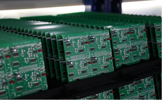
Types of PCBA Tests: In-Circuit, Functional, and AOI Testing Overview
Every electronic product, from industrial controllers to wearable devices, depends on the flawless performance of its printed circuit board assembly. Yet, even a tiny solder bridge or a misaligned chip can compromise reliability long before the product reaches the user. Ensuring that each board functions perfectly requires a series of rigorous PCBA tests that reveal hidden faults and verify performance at every stage of production.
Among the many testing methods available, three stand out for their precision and effectiveness—In-Circuit Test (ICT), Functional Test (FCT), and Automated Optical Inspection (AOI). Each plays a distinct role in safeguarding quality, from detecting electrical issues to confirming that every circuit behaves exactly as intended.
In-Circuit Test (ICT): Component-Level Verification
What Is In-Circuit Testing?
In-Circuit Testing (ICT) is a method used to verify the electrical performance and connectivity of individual components on a printed circuit board assembly (PCBA).
It uses a bed-of-nails fixture or flying probe system to make direct contact with test points on the board. Each probe sends a signal that checks whether components such as resistors, capacitors, and diodes meet their specified electrical values.
ICT focuses on the component level, not the overall function of the product. It ensures that every part is correctly placed, properly soldered, and electrically sound before the board is powered on.
Common ICT systems include Keysight 3070 and Teradyne TestStation, which are widely used in high-volume electronics manufacturing for their precision and speed.
How ICT Works
The ICT process combines automated electrical measurements with component-level diagnostics. Here’s how it typically operates:
1. Contact setup: The PCB is placed on a test fixture (bed-of-nails) or under a flying probe machine.
2. Signal application: Electrical probes send controlled signals through each component and track the response.
3. Parameter measurement: The system measures values such as resistance, capacitance, voltage drop, and current flow.
4. Fault detection: Deviations from expected values indicate issues like short circuits, open circuits, missing components, or incorrect polarity.
5. Result output: The test system generates a pass/fail report, pinpointing exact defect locations for repair.
ICT is typically performed after PCB assembly but before power-on, reducing the risk of damage to the circuit during later functional testing.
Advantages and Limitations
Advantages of In-Circuit Testing:
High fault coverage: Detects most manufacturing defects at the component level.
Speed and automation: Once the fixture is built, tests can be run quickly with minimal operator intervention.
Accurate diagnostics: Provides precise fault location data, simplifying rework and quality control.
Limitations of In-Circuit Testing:
High setup cost: Requires a custom test fixture, which can be expensive for low-volume production.
Limited flexibility: Fixture design changes are time-consuming if the PCB layout is modified.
Not ideal for prototypes or frequent design changes, where flying probe tests may be more cost-effective.
In short, ICT is best suited for mass production environments where the same PCB design is tested repeatedly and consistency is critical.
Example Application
Consider an automotive control PCB that manages engine performance. To ensure safety and reliability, each resistor and capacitor must operate within its specified tolerance.
A typical ICT workflow follows these steps:
1. Fixture alignment: The board is positioned so that each test pin aligns with its designated test pad.
2. Electrical probing: The system sequentially applies test signals to check component values and connections.
3. Data capture: Results are automatically logged for traceability.
4. Analysis and reporting: The software generates a pass/fail report, highlighting specific defective components if detected.
Through this process, manufacturers can confirm that every electrical path on the PCB is correct before moving to functional or optical tests, ensuring the product’s integrity from the earliest testing stage.
Functional Test (FCT): System-Level Validation
What Is Functional Testing?
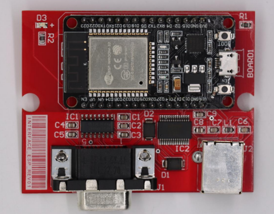
Functional Testing (FCT) is a method used to evaluate whether a fully assembled printed circuit board assembly (PCBA) performs its intended function under real or simulated operating conditions.
Unlike In-Circuit Testing (ICT), which focuses on individual components, FCT verifies the overall performance of the complete system.
Functional testing is often referred to as a system test or end-of-line test because it typically occurs at the final stage of production—after all assembly and programming are complete. Its goal is to confirm that the PCBA behaves exactly as it would in the final product environment, ensuring that both hardware and firmware work together correctly.
How Functional Testing Works
The functional test process simulates the real-world conditions in which the PCB will operate. Here’s how it typically works:
1. Power and connection setup:
The PCBA is powered on and connected to dedicated test equipment, which may include software interfaces, sensors, or external load simulators.
2. Signal monitoring and measurement:
The system checks output signals, verifies communication protocols (such as UART, I²C, SPI, or Ethernet), and measures performance under load to ensure the circuit meets design specifications.
3. Functional scenario simulation:
Environmental simulations—such as temperature, vibration, or voltage fluctuations—can be introduced to test reliability under stress.
4. Data logging and analysis:
Test software records results, compares them to expected values, and generates a pass/fail report highlighting any operational defects.
Functional testing helps verify not just connectivity, but also logic control, timing accuracy, and firmware execution. It provides a final assurance that the assembled board is production-ready.
Advantages and Limitations
Advantages of Functional Testing:
Real-world validation: Confirms that the assembled PCBA performs as intended under operational conditions.
Comprehensive detection: Identifies faults related to firmware, soldering, and interface behavior that electrical tests cannot detect.
Customer assurance: Ensures that end users receive a product that meets full performance and reliability standards.
Limitations of Functional Testing:
Time and setup cost: Requires detailed test programming, setup of custom fixtures, and longer testing cycles.
Complex test design: Must replicate the product’s actual environment, which can be challenging for highly integrated systems.
Limited root-cause insight: While FCT can confirm a failure, it may not always identify which specific component caused it—this often requires earlier-stage tests like ICT.
In practice, functional testing complements other inspection methods, serving as the final checkpoint before shipment.
Example Use Case
Consider a Wi-Fi router PCB as an example. After assembly and firmware programming, the board must be tested to verify its functional performance.
A typical FCT sequence might include:
1. Power-up validation: Ensures stable startup and proper current draw.
2. Signal verification: Checks Wi-Fi signal transmission and reception at defined frequencies.
3. Interface testing: Confirms correct operation of Ethernet ports, USB connections, and LED indicators.
4. Firmware confirmation: Verifies successful boot sequence and correct software version.
5. Performance evaluation: Runs load tests to ensure consistent data throughput and temperature stability.
Through this process, engineers can confirm that the router board behaves exactly as expected—functionally stable, fully integrated, and ready for end-user deployment.
Automated Optical Inspection (AOI): Visual and Structural Accuracy
What Is AOI Testing?
Automated Optical Inspection (AOI) is a non-contact visual inspection process that uses high-resolution cameras and intelligent image-processing algorithms to identify assembly defects on a printed circuit board assembly (PCBA).
It visually examines the surface of the board, capturing precise images to ensure that every component is correctly placed, aligned, and soldered.
AOI is typically performed after solder paste printing and reflow soldering, when most visible defects—such as misaligned parts, solder bridges, or missing components—can occur. Because it relies on optical data rather than electrical signals, AOI is one of the fastest and most reliable tools for early defect detection in modern PCB manufacturing.
How AOI Works
The AOI inspection process combines optical imaging with automated pattern recognition. It generally follows these steps:
1. Image capture:
The system uses multiple 2D or 3D cameras to scan the entire surface of the PCBA, creating detailed images of component placement and solder joints.
2. Reference comparison:
Captured images are compared to a “golden board”—a reference model of a perfect assembly. The AOI software analyzes pixel-level differences to identify irregularities.
3. Defect detection:
Advanced algorithms detect common visual issues such as solder bridges, tombstoned components, incorrect polarity, missing parts, or misalignments.
4. Verification and reporting:
Any potential defects are flagged for operator review, and the system generates a detailed inspection report with defect location and type.
AOI can be used both inline (integrated directly into the production line) and offline (stand-alone analysis), depending on production scale and workflow requirements.
Advantages and Limitations
Advantages of AOI Testing:
Fast and non-destructive: AOI inspects every board visually without physical contact or power application.
High accuracy: Detects small visual defects that human eyes might miss, ensuring consistent quality.
Inline integration: Ideal for high-volume production, where immediate feedback helps reduce downstream rework.
Early defect prevention: Identifies problems right after soldering, preventing defective boards from moving further in the process.
Limitations of AOI Testing:
Electrical limitations: AOI cannot verify electrical performance or detect internal faults such as open circuits.
Algorithm sensitivity: Poor lighting, incorrect camera calibration, or tight tolerance settings can cause false positives or missed defects.
Complex board designs: Dense or multi-layer PCBs may require 3D AOI systems to accurately evaluate solder joints.
Despite these challenges, AOI remains an essential tool for ensuring visual and structural integrity before electrical testing begins.
Example Application
A typical use case for AOI is in smartphone mainboard production, where precision is critical.
During inspection, the AOI system scans each assembled board immediately after reflow soldering. It detects:
A misaligned integrated circuit (IC) that could cause poor contact or shorting.
Insufficient solder paste on micro-pads that might lead to intermittent connections.
Reversed polarity components, such as capacitors or LEDs, which would fail functional tests later.
By identifying these issues early, manufacturers can correct process errors in real time—reducing scrap rates, improving yield, and ensuring consistent product quality across large production runs.
Comparative Analysis: ICT vs. FCT vs. AOI
Key Differences
Understanding the distinctions between In-Circuit Testing (ICT), Functional Testing (FCT), and Automated Optical Inspection (AOI) is essential for designing an effective PCBA quality strategy.
Focus:
ICT emphasizes electrical integrity, verifying that each component is correctly connected and meets specified values.
FCT focuses on functional performance, confirming that the assembled board operates correctly in real-world conditions.
AOI is dedicated to visual and structural quality, detecting misaligned components, solder defects, and polarity errors.
Stage of Use:
AOI is generally performed early or mid-process, right after solder paste printing and reflow soldering.
ICT and FCT are conducted post-assembly, with ICT often preceding FCT to identify component-level faults before system-level validation.
Type of Defects Detected:
Test Type | Primary Focus | Defects Detected |
|---|---|---|
AOI | Visual/structural | Misaligned components, missing parts, solder bridges, polarity errors |
ICT | Electrical/component | Short circuits, open circuits, wrong or missing components, incorrect values |
FCT | Functional/system | Firmware errors, interface issues, signal integrity problems, load performance failures |
This table summarizes the unique strengths and limitations of each test type, helping engineers quickly identify which method addresses specific quality concerns.
When to Use Each Test
Selecting the right test depends on product complexity, production stage, and defect type:
AOI: Ideal for early defect prevention, catching visual issues before electrical testing begins.
ICT: Most effective in volume production where repeatable test setups can efficiently verify every component.
FCT: Best suited for final product validation, confirming that the board performs correctly under operational conditions before shipment.
By aligning test selection with production goals, manufacturers can minimize defects, reduce rework, and maintain consistent quality.
Combining Multiple Tests for Maximum Coverage
For comprehensive quality assurance, many manufacturers integrate AOI, ICT, and FCT into a sequential workflow:
1. AOI: Detects visual defects immediately after soldering.
2. ICT: Confirms component-level electrical integrity.
3. FCT: Validates system-level performance and functionality.
Example: A consumer electronics company producing smart home devices uses this three-tier approach. AOI identifies missing or misaligned micro-components, ICT ensures correct resistor and capacitor values, and FCT validates network communication and firmware operation. This integrated workflow can achieve up to 99% defect coverage, reducing returns and improving customer satisfaction.
Combining these tests leverages the strengths of each method, ensuring both component accuracy and system reliability, while preventing defective boards from reaching the end user.
Choosing the Right PCBA Testing Strategy
Selecting an effective PCBA testing strategy requires balancing product requirements, production goals, and resource constraints. The right approach ensures high quality, reliability, and cost-efficiency throughout the manufacturing process.
Factors to Consider
1. Product Complexity and Production Volume
Complex boards with multiple layers, high-density components, or embedded systems may require a combination of AOI, ICT, and FCT to ensure complete defect coverage.
High-volume production benefits from automated testing, such as AOI and ICT fixtures, to maintain consistent throughput.
Low-volume or prototype boards may rely more on flying probe ICT or selective functional tests to reduce setup costs.
2. Cost and Time Constraints
Test strategy should balance accuracy, speed, and budget.
AOI offers rapid inline inspection, minimizing rework costs.
ICT requires a fixture investment, which is cost-effective only for repeated production runs.
FCT, while slower, ensures system-level verification before shipment, preventing expensive field failures.
3. Quality Requirements and Customer Standards
Products with strict reliability requirements—such as medical devices or automotive electronics—demand high fault coverage and adherence to industry standards (IPC, ISO, or customer-specific specs).
Customer expectations may dictate a specific combination of visual, electrical, and functional testing to meet contractual quality levels.
Best Practices for Implementation
1. Integrate Test Planning in the Design for Testability (DFT) Stage
Incorporate test points, accessibility, and fixture compatibility during the PCB design phase.
Early planning reduces later rework and ensures that ICT, AOI, and FCT can be applied efficiently.
2. Maintain Calibration and Periodic Validation of Test Equipment
Regularly calibrate AOI cameras, ICT fixtures, and functional test systems to maintain measurement accuracy.
Schedule preventive maintenance to avoid false positives, misalignments, or overlooked defects.
3. Use Data from Test Results for Continuous Process Improvement
Analyze defect trends to identify recurring issues, such as soldering errors or component misplacement.
Feed insights back into assembly processes, supplier quality control, and design adjustments.
Over time, this approach reduces scrap rates, increases yield, and strengthens overall product reliability.
By carefully considering complexity, cost, and quality requirements, and by implementing these best practices, manufacturers can develop a PCBA testing strategy that ensures high product reliability, minimized defects, and optimized production efficiency.
Conclusion
Effective PCBA testing is essential for ensuring product reliability and performance. Each test type serves a unique role: AOI identifies visual and structural defects, ICT verifies electrical integrity at the component level, and FCT validates system-level functionality under real-world conditions. Using the right combination of these methods helps manufacturers catch defects early, reduce rework, and deliver consistently high-quality products.
Selecting an appropriate testing strategy depends on factors such as product complexity, production volume, cost constraints, and quality standards. Integrating AOI, ICT, and FCT in a well-planned workflow maximizes defect coverage and ensures both component accuracy and overall system performance.
At PCBMASTER, quality is a top priority. Every PCBA provided undergoes rigorous, comprehensive testing to meet stringent industry standards and customer expectations. From properly calibrated AOI cameras to precise ICT fixtures and reliable functional test protocols, PCBMASTER ensures that every board leaving the facility is verified for accuracy, functionality, and durability.
For further insights into optimizing PCBA testing, related topics such as ICT fixture design, FCT software development, and AOI camera calibration provide practical guidance for improving production efficiency and product reliability.
FAQs
1. What are the main differences between ICT and functional testing?
In-Circuit Testing (ICT) and Functional Testing (FCT) serve different purposes in PCBA quality assurance. ICT focuses on component-level electrical verification, checking for short circuits, open circuits, incorrect resistor or capacitor values, and missing components before the board is powered on. FCT, on the other hand, evaluates the system-level performance of the assembled PCB under simulated operating conditions, detecting firmware issues, signal integrity problems, and interface failures. Simply put, ICT ensures each individual component works correctly, while FCT ensures the entire board functions as intended.
2. Can AOI testing replace in-circuit or functional testing?
Automated Optical Inspection (AOI) cannot replace ICT or FCT. AOI specializes in visual and structural inspection, identifying defects like misaligned components, missing parts, solder bridges, and incorrect polarity. However, AOI does not assess electrical connectivity or system functionality. For comprehensive PCBA testing, AOI should be combined with ICT and FCT to ensure boards are both structurally accurate and electrically reliable.
3. How early should PCBA testing be planned in the manufacturing process?
Effective PCBA testing should be planned during the PCB design phase, particularly in the Design for Testability (DFT) stage. Early planning ensures adequate test points for ICT and FCT, compatibility with AOI inspection, and reduced risk of costly rework. Boards designed with testing in mind allow for smoother production, faster defect detection, and higher manufacturing yield, making early integration critical for both prototypes and mass production.
4. What types of defects can’t AOI testing detect?
AOI is limited to visual inspection, so it cannot detect electrical or functional defects. This includes open or short circuits, incorrect component values, firmware errors, signal integrity problems, and performance failures under load or environmental stress. As a result, relying solely on AOI leaves critical functional issues undetected, highlighting the need to pair AOI with ICT and FCT for comprehensive PCBA quality assurance.
5. Is in-circuit testing suitable for low-volume or prototype PCBAs?
Standard ICT is generally not ideal for low-volume or prototype PCBA production because it requires custom test fixtures, which are expensive and time-consuming to develop. For small batches or prototypes, flying probe ICT or selective functional tests offer a practical solution, providing reliable component-level verification without high fixture costs. ICT is most effective in high-volume, repeatable production, where test fixtures can be reused across multiple boards.

