


End-to-End Turn-Key PCB Manufacturing & Assembly for Complex Designs
Every trace, via, and layer in a high-performance PCB plays a critical role—and even the smallest misstep can ripple across an entire system. For projects that demand precision, complexity, and reliability, standard approaches are no longer enough. Advanced turn-key solutions are stepping in to bridge the gap between design ambition and real-world performance.
Understanding Full Turn-Key PCB Solutions in Modern Electronics
What “Full Turn-Key” Really Means
A full turn-key PCB solution refers to a manufacturing approach that covers every step of the PCB lifecycle, from initial design to final delivery. This end-to-end process typically includes:
Engineering and design: creating schematics, layouts, and performing simulations.
Fabrication: producing the PCB with precise materials, layers, and high-density interconnects (HDI).
Assembly: placing and soldering components, whether through SMT or THT techniques.
Testing: verifying electrical performance, signal integrity, and functional reliability.
Delivery: providing ready-to-use boards that meet customer specifications.
Unlike partial turn-key models, which only cover some stages (for example, fabrication only), or consignment models, where clients supply components and oversee parts of the process, full turn-key services manage everything under one roof. This approach offers multiple advantages:
Single-source management: one point of contact reduces coordination errors and streamlines communication.
Shorter production cycles: integrated workflows allow faster transition from design to delivery.
Stable, predictable quality: standardized processes ensure every board meets industry requirements consistently.
Example: A company developing a 16-layer HDI PCB with blind and buried vias benefits from full turn-key service because the design team, fabrication, and assembly lines are all coordinated, minimizing errors and rework.
Why High-Difficulty PCBs Demand Full Turn-Key
High-difficulty PCBs, such as HDI boards, rigid-flex circuits, and high-speed multilayer designs, involve complex structures that require precise engineering and tightly controlled manufacturing processes. Full turn-key solutions are particularly important because:
1. Synchronized design and production
Complex stack-ups and microvias demand that engineers and manufacturers work together from
the start.
Example: A misalignment in a 32-layer HDI board can cause signal interference; turn-key management ensures design intent is maintained during fabrication.
2. Material compatibility and tolerance control
High-frequency laminates, metal cores, and flexible substrates have specific handling requirements.
A turn-key provider manages these across the entire workflow, ensuring consistent thickness, impedance, and thermal performance.
3. Reduced risk of miscommunication and errors
Multiple handoffs between independent vendors often cause delays or defects.
Full turn-key integration keeps all teams aligned, preventing costly mistakes before assembly or testing.
Example: In a rigid-flex PCB used in wearable medical devices, synchronized design and assembly under a full turn-key provider prevent delamination and ensure that bending areas function reliably throughout the product lifecycle.
Engineering-Driven PCB Design Support
Collaborative Design Approach
Effective PCB design begins with close collaboration between the engineering team and the customer. This starts with gathering requirements and conducting a feasibility review to ensure that the intended design is achievable within material, process, and performance constraints.
Early involvement in Design for Manufacturability (DFM) and Design for Testability (DFT) is critical. By identifying potential manufacturing or testing challenges during the design phase, engineers can make adjustments before production, reducing costly redesigns and improving first-pass yield.
Example: For a high-speed HDI PCB intended for a networking router, early DFM/DFT checks ensure that microvias are properly placed and test points are accessible, preventing rework during assembly and testing.
Advanced Engineering Capabilities
Modern PCB projects, especially high-speed and high-density designs, require sophisticated engineering tools and techniques:
Signal integrity (SI) simulation: Engineers simulate how signals travel through traces and vias, identifying potential issues like reflections, crosstalk, or skew.
Stack-up optimization: Layer arrangement is carefully planned to balance controlled impedance, thermal management, and mechanical reliability.
Example: In 28–112Gbps backplane PCBs, SI analysis can prevent timing skew and crosstalk by adjusting trace lengths, spacing, and via placement. This ensures the board meets strict high-speed signal requirements without repeated prototyping.
Additional engineering services may include thermal simulations, EMI predictions, and power integrity analysis, all integrated to maximize PCB performance and reliability.
Documentation and Pre-Production Reviews
Before fabrication, documentation and pre-production checks are essential to catch potential errors:
Gerber/DXF review: Verifies that layout files accurately reflect the design intent and comply with manufacturing capabilities.
CAM optimization: Computer-aided manufacturing tools check trace widths, spacing, drill sizes, and layer alignment.
Manufacturability checks: Ensure the design can be produced efficiently without quality compromises, including reviewing tolerances for high-density features.
Step-by-step example:
1. Gerber files are loaded into CAM software.
2. Trace widths and spacing are verified against fabrication capabilities.
3. Drill sizes and via positions are checked for feasibility.
4. Any potential errors are flagged for review and correction before production.
This structured review process ensures that high-difficulty PCBs are ready for fabrication and assembly with minimal risk, maintaining consistent quality and performance.
Accelerated Prototyping Workflow
Quick-Turn Fabrication
Rapid prototyping is a cornerstone of modern PCB development, allowing engineers to test and iterate designs quickly. Quick-turn fabrication leverages advanced processes such as:
Fast tooling setup: Minimizes preparation time for machinery and materials.
Laser Direct Imaging (LDI): Precisely transfers high-resolution circuit patterns onto PCB substrates.
Digital drill programming: Automates via and hole placement with micron-level accuracy.
Lead time considerations:
Simple prototypes (2–4 layers, standard materials) can often be produced in 1–3 days.
Complex prototypes (HDI, rigid-flex, high layer count) may require 5–10 days, depending on stack-up, vias, and material requirements.
This accelerated fabrication approach reduces development cycles, enabling faster evaluation of design performance before full-scale production.
Component Sourcing Integration
Effective prototyping is not just about the board—it also depends on the availability and compatibility of components. Key steps include:
BOM validation: Ensures all components are correctly specified and available.
Supplier screening: Identifies reliable vendors for quality and lead time.
Lifecycle checks: Confirms components are not nearing End-of-Life (EOL).
By integrating component sourcing early in the prototyping phase, engineers avoid redesigns caused by unavailable or obsolete parts, saving time and cost.
Example: A 16-layer HDI PCB prototype could fail if a critical BGA component is discontinued; early sourcing prevents delays and design changes.
Prototype Assembly & Debugging
Once fabrication and components are ready, prototype assembly and debugging validate the design under real-world conditions:
Trial assembly: Tests placement and soldering for BGAs, QFNs, and fine-pitch components.
Rework and verification: Defective areas are corrected and retested.
Engineering feedback loop: Iterative adjustments are made based on functional testing.
Example: For a wearable rigid-flex PCB, multiple prototype cycles allow engineers to optimize bend areas, test electrical continuity, and ensure durability under repeated motion.
Step-by-step cycle:
1. Fabricate prototype PCB.
2. Source and assemble components.
3. Perform functional and mechanical testing.
4. Apply feedback to refine layout or materials.
5. Repeat until performance meets specifications.
This workflow ensures that high-complexity PCBs are validated before mass production, reducing the risk of costly errors and ensuring reliable final products.
Capabilities for High-Difficulty PCB Manufacturing
Complex PCB Types Supported
High-difficulty PCBs require specialized manufacturing processes to meet demanding performance and reliability standards. Some of the key types include:
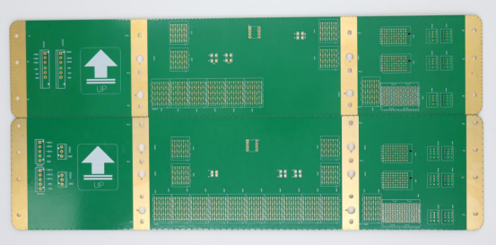
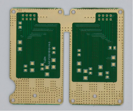
HDI (High-Density Interconnect) PCBs: Structures such as 1+N+1, 2+N+2, and stacked vias allow for higher component density and shorter signal paths. These designs are essential in smartphones, networking equipment, and high-speed computing devices.
Rigid-flex & dynamic flex circuits: Combine rigid PCB sections with flexible areas, enabling compact, foldable designs for wearables, medical devices, and aerospace applications.
High-frequency RF/microwave PCBs: Designed for minimal signal loss and stable performance at GHz frequencies, used in radar systems, wireless communication, and high-speed data links.
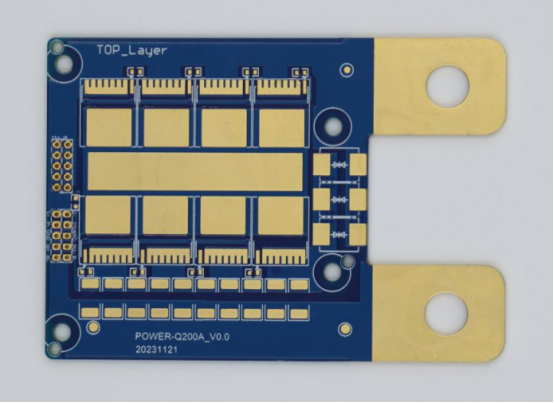
Metal-core and thermal-dissipation PCBs: Incorporate metal substrates to improve heat dissipation for LED lighting, power electronics, and high-current applications.
Example: A wearable medical monitor may use a rigid-flex PCB to maintain electrical connectivity while bending around the wrist, combining multiple HDI layers for compact functionality.
Precision Fabrication Technologies
Advanced manufacturing techniques are essential to achieve the fine tolerances required by high-difficulty PCBs:
Fine line/space capability: Trace widths and spacing can reach as low as 2–3 mils, allowing higher routing density.
Laser drilling for microvias: Enables precise creation of vias as small as 75–100 μm, critical for stacked HDI structures.
Controlled dielectric thickness and impedance control: Ensures signal integrity in high-speed and RF applications, maintaining consistent impedance across the board.
Step-by-step insight:
1. PCB stack-up is defined for signal routing and layer count.
2. Laser drilling creates microvias with micron-level accuracy.
3. Controlled dielectric materials are applied to maintain impedance and minimize crosstalk.
4. Fine-line traces are patterned using high-resolution imaging techniques.
These techniques collectively ensure high yield, electrical performance, and reliability in complex PCBs.
Material Expertise
Selecting the right materials is crucial for high-difficulty PCBs to perform under electrical, thermal, and mechanical stresses:
High-performance FR4 and high-Tg laminates: Megtron, Isola, Shengyi, offering low dielectric loss and thermal stability for high-speed signals.
Advanced materials: PTFE, ceramic-filled substrates, and metal-backed laminates for RF applications or thermal management.
Comparison – High-speed laminates vs. standard FR4:
- High-speed laminates: Lower dielectric constant (Dk), lower loss tangent (Df), suitable for GHz signals.
- Standard FR4: Higher Dk and Df, suitable for conventional digital circuits but may cause signal degradation at high frequencies.
Example: A 28-layer HDI RF PCB for a 5G base station may use Megtron laminates for controlled impedance, while a standard FR4 board would fail to meet signal integrity requirements at the same frequency.
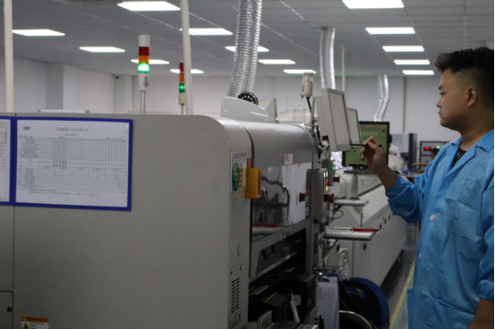
Advanced PCB Assembly & Process Control
SMT and THT Capabilities
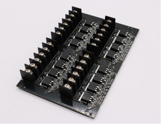
Modern high-difficulty PCBs demand precise assembly methods to ensure performance and reliability. Our assembly capabilities cover both Surface Mount Technology (SMT) and Through-Hole Technology (THT):
High-precision placement: Components as small as 01005 resistors and μBGA packages are accurately positioned using advanced pick-and-place equipment.
Mixed-technology assembly flows: SMT and THT processes are integrated in a single workflow, accommodating a wide variety of components and package types without compromising throughput or quality.
Example: A 32-layer HDI PCB for a high-speed networking module may include fine-pitch μBGAs alongside larger THT connectors. Combining SMT and THT ensures proper placement, soldering, and connectivity across all components.
Inspection and Test Systems
To guarantee quality and detect defects early, multiple inspection and testing techniques are employed:
Automated Optical Inspection (AOI): Detects soldering defects, missing components, or misalignments quickly and accurately.
X-ray inspection: Reveals hidden issues in BGA pads, via-in-pad structures, and multilayer connections that AOI cannot detect.
Electrical testing workflows:
- In-Circuit Testing (ICT) checks each component’s electrical functionality.
- Functional Circuit Testing (FCT) verifies the overall PCB operation under simulated working conditions.
- Boundary-scan testing identifies faults in high-density, high-speed PCBs without physical probing.
Step-by-step example:
1. AOI inspects solder joints immediately after reflow.
2. X-ray scans confirm hidden vias and BGA solder quality.
3. ICT or FCT validates electrical performance before shipping.
This layered approach ensures high reliability and first-pass yield, especially in complex and high-speed PCBs.
Post-Assembly Reliability Enhancements
High-performance PCBs often face challenging environments. To improve durability and longevity, the following post-assembly techniques are applied:
Conformal coating: Protective layer applied over the PCB surface to resist moisture, dust, and corrosion.
Potting and underfill: Encapsulates sensitive components or BGAs, providing mechanical stability and thermal conduction.
Environmental stress testing: Includes thermal cycling, vibration, and humidity tests to validate the board’s robustness under extreme conditions.
Example: A rigid-flex PCB used in wearable medical devices undergoes thermal cycling and vibration tests to ensure bend areas and solder joints maintain integrity over repeated use.
Technology Investments That Enable High-Complexity Builds
Fabrication Technologies
Manufacturing high-complexity PCBs requires advanced fabrication technologies that ensure precision, reliability, and repeatability:
Laser Direct Imaging (LDI): Provides high-resolution patterning for fine traces, microvias, and high-density interconnects (HDI), reducing registration errors.
CNC and laser routing systems: Enable precise cutting, shaping, and routing of PCBs, including complex outlines, slots, and flexible sections.
Plasma treatment for adhesion enhancement: Improves surface energy of laminates and metals, ensuring solder masks, coatings, and adhesives bond consistently.
Example: An HDI PCB with stacked microvias relies on LDI imaging to maintain layer alignment, minimizing defects that could occur with traditional phototools.
Testing and Measurement Tools
High-complexity boards require specialized testing and measurement equipment to validate performance before assembly or deployment:
High-frequency impedance testers: Measure controlled impedance across traces to ensure signal integrity, critical for RF, microwave, and 5G applications.
Flying probe testers: Ideal for prototype validation or low-volume production, detecting shorts, opens, and component misplacements without requiring dedicated test fixtures.
Step-by-step example:
1. Fabricated PCB is placed under a flying probe tester.
2. Electrical continuity and isolation are verified.
3. Impedance measurements are cross-checked against design specifications.
4. Any deviations are flagged for correction before assembly.
Examples of Process Control Advantages
Advanced technologies directly improve manufacturing accuracy and PCB reliability:
LDI reduces registration errors in HDI boards: By providing precise image transfer, LDI ensures microvias and fine traces align correctly across multiple layers, improving yield.
5G PCBs benefit from precise impedance verification: Accurate impedance control prevents signal loss and crosstalk in high-speed RF paths, ensuring performance in demanding communication systems.
Comparison: Without LDI and high-frequency measurement tools, HDI and high-speed boards are more prone to layer misalignment, impedance mismatch, and rework, increasing cost and development time.
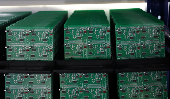
End-to-End Quality Management Framework
Certifications and Standards
Maintaining consistent quality in high-difficulty PCB manufacturing requires compliance with internationally recognized standards:
ISO 9001: Ensures comprehensive quality management systems across design, fabrication, and assembly.
ISO 13485: Addresses quality requirements specific to medical devices, emphasizing risk management and traceability.
IPC-A-600 & IPC-A-610: Define acceptability criteria for PCB fabrication and assembly, including solder joint quality, surface finishes, and layer integrity.
For medical, aerospace, and high-reliability applications, traceability is critical. Each PCB batch is documented from material receipt to final delivery, ensuring compliance with regulatory audits and customer requirements.
Example: A medical device PCB must retain full traceability of laminates, components, and assembly processes to meet ISO 13485 audits, allowing defect tracking and corrective action.
Inline Quality Monitoring
Quality is continuously verified during production through inline monitoring systems:
Statistical Process Control (SPC) and process logs: Track key parameters such as solder temperature, pick-and-place accuracy, and assembly yield in real time.
Defect root-cause analysis and continuous improvement loops: When a deviation is detected, engineers investigate the source, apply corrective measures, and update procedures to prevent recurrence.
Step-by-step example:
1. A defect in solder joints is detected during AOI inspection.
2. SPC logs reveal a slight deviation in reflow temperature.
3. Process parameters are adjusted, and subsequent boards are verified.
4. Findings are documented, feeding into continuous improvement initiatives.
This approach reduces variability, prevents recurring errors, and improves overall first-pass yield.
Final Product Validation
Before shipment, each PCB undergoes comprehensive final testing and validation:
Electrical testing: Confirms connectivity, short/open circuits, and impedance compliance.
Functional tests: Simulate operational conditions to ensure proper performance of all circuits and components.
Customer acceptance reports: Document inspection results, test data, and compliance with specifications.
Example: For a 28-layer HDI PCB used in aerospace avionics, electrical testing ensures signal integrity and correct voltage levels across all high-speed traces, while functional tests validate system-level performance before delivery.
This structured framework ensures that every PCB meets high reliability standards, regardless of complexity, industry, or application.
Choosing a Turn-Key Partner for High-Difficulty PCB Projects
Criteria to Evaluate a Supplier
Selecting the right partner is critical for high-difficulty PCB projects. Key factors include:
Capability vs. complexity alignment: Ensure the supplier can handle the required PCB types, such as HDI, rigid-flex, high-frequency, or metal-core boards. Suppliers should demonstrate experience in multi-layer and high-density designs.
Material portfolio and HDI expertise: A broad selection of laminates and high-speed substrates, along with expertise in stacked or blind/buried vias, ensures compatibility with complex designs.
Lead time competitiveness: Efficient production workflows and quick-turn prototyping reduce time-to-market, critical for rapid development cycles.
Example: For a 32-layer HDI PCB with blind and buried vias, a supplier with proven HDI experience and a stock of high-Tg and high-speed laminates reduces redesign risks and ensures on-time delivery.
Common Pitfalls When Outsourcing PCB Production
Outsourcing PCB manufacturing carries risks if not carefully managed:
Multi-supplier misalignment: Using separate vendors for fabrication, assembly, and components can lead to miscommunication, inconsistent quality, and delayed schedules.
Insufficient DFM involvement: Early-stage design-for-manufacturability review is critical. Without it, complex PCBs may require redesigns during production, increasing cost and time.
Comparison: A multi-vendor approach may require multiple engineering touchpoints and increase error probability, whereas a single turn-key partner simplifies communication and reduces risks.
How Full Turn-Key Improves Long-Term Project Reliability
Partnering with a full turn-key provider brings measurable benefits:
Stable supply chain: Integrated sourcing, fabrication, and assembly reduce dependency on external vendors and ensure continuity of materials and components.
Predictable quality and fewer engineering changes: Continuous engineering oversight from design to delivery minimizes defects, rework, and variations, improving product reliability over time.
Example: A high-speed PCB project using a full turn-key supplier experiences consistent impedance control, reduced assembly errors, and faster iterations compared to coordinating multiple separate vendors.
Why Choose PCBMASTER for Complex PCB Projects
When selecting a turn-key partner for complex PCB projects, PCBMASTER stands out for its comprehensive capabilities and proven expertise. Here’s why:
Comprehensive one-stop services: PCBMASTER covers design, quick-turn prototyping, assembly, and component sourcing, ensuring smooth coordination across all stages of production.
Advanced PCB capabilities: Supports HDI, rigid-flex, high-frequency, metal-core, and mini-LED boards, with fine-line traces down to 2 mils, and multi-layer high-density designs.
Rigorous quality assurance: Fully compliant with ISO 9001, IATF 16949, and UL standards, each board undergoes strict inspection to guarantee consistent quality and reliability.
Efficient and customer-focused service: 24/7 online support, free engineering document checking, transparent pricing, and a 99% on-time delivery rate ensure smooth project execution.
Proven global experience: PCBMASTER has served thousands of enterprises across consumer electronics, industrial control, automotive, communication, and medical fields, demonstrating a strong track record in high-difficulty PCB projects.
Example: A multi-layer HDI PCB for a wearable medical device moved from prototype to mass production with minimal redesigns, consistent quality, and faster time-to-market, thanks to PCBMASTER’s integrated turn-key approach.
Conclusion
Delivering high-performance, high-difficulty PCBs requires more than advanced materials and equipment—it demands an integrated, turn-key approach. From collaborative design and rapid prototyping to precision manufacturing, assembly, and rigorous quality assurance, every step impacts reliability, performance, and time-to-market.
Partnering with a full turn-key provider like PCBMASTER ensures seamless coordination, stable supply chains, and consistent quality across complex PCB projects. With deep expertise in HDI, rigid-flex, high-frequency, and metal-core boards, PCBMASTER helps innovators turn challenging designs into reliable products efficiently.
Whether you are developing next-generation consumer electronics, industrial systems, or medical devices, leveraging a comprehensive turn-key PCB solution minimizes risks, reduces iterations, and accelerates innovation—giving your project a competitive edge from prototype to mass production.
FAQs
What is the difference between full turn-key and partial turn-key PCB services?
Full turn-key PCB services cover the entire production workflow: design, prototyping, fabrication, assembly, component sourcing, and final testing. Partial turn-key or consignment services involve only specific stages, such as assembly or sourcing, requiring coordination with multiple vendors. Full turn-key reduces miscommunication, shortens lead times, and ensures consistent quality throughout the project.
How does HDI PCB manufacturing improve performance in high-speed devices?
HDI (High-Density Interconnect) PCBs use stacked or microvias, finer lines, and higher layer counts, enabling shorter signal paths, reduced parasitic capacitance, and better signal integrity. These features are critical for high-speed devices, such as 5G modules or networking equipment, as they minimize crosstalk and signal loss while supporting compact designs.
Why is controlled impedance important in advanced PCB designs?
Controlled impedance ensures consistent electrical characteristics along high-speed signal traces. Variations in impedance can cause reflections, signal degradation, or timing errors, particularly in RF, high-speed digital, and high-frequency circuits. Maintaining precise impedance is essential for signal integrity, reliable communication, and predictable device performance.
What testing methods ensure reliability in complex PCB assemblies?
Reliability is verified through multiple inspection and testing methods:
AOI (Automated Optical Inspection) for solder joint and component placement defects.
X-ray inspection for hidden pads, BGAs, and via-in-pad structures.
ICT (In-Circuit Testing) and FCT (Functional Circuit Testing) to check electrical performance.
Boundary-scan testing for high-density boards without physical probing.
Environmental stress testing (thermal cycling, vibration) for durability under extreme conditions.
Which industries benefit the most from full turn-key PCB services?
Full turn-key PCB services are especially valuable for industries requiring high reliability, complex designs, and fast time-to-market, including:
Consumer electronics (smartphones, wearables)
Industrial control and automation
Automotive electronics (ADAS, EV modules)
Medical devices and wearable health monitors
Telecommunications and networking equipment (5G, RF modules)

