


Flexible PCB EMI Shields: How to Minimize Interference and Boost Reliability
In today’s world, electronic devices are everywhere, quietly humming and communicating around us. Yet, hidden beneath their sleek surfaces lies a constant struggle—signals crossing paths, wires radiating, and interference creeping in. For flexible printed circuit boards, this invisible battle can compromise performance, disrupt sensitive electronics, and create unexpected failures. Understanding how to control electromagnetic interference isn’t just a technical necessity—it’s the key to designing flex circuits that perform reliably in a complex electronic environment.
Introduction to EMI in Flex PCBs
What is Electromagnetic Interference (EMI)?
Electromagnetic interference, or EMI, refers to the unwanted disturbance of electronic signals caused by electromagnetic radiation from nearby devices. Essentially, it is “noise” that disrupts the normal operation of electronics. A simple example can be seen when you turn on a TV while listening to the radio—the TV signal can interfere with the radio, producing static or distortion. Similarly, when boarding an airplane, passengers are often asked to switch off mobile devices. This precaution prevents EMI from interfering with the aircraft’s navigational and communication systems.
EMI is not just a minor annoyance; it can cause errors in data transmission, degrade audio or video quality, and in critical systems, even pose safety risks. Effective EMI control ensures that devices operate reliably in environments with multiple electronic systems nearby. Controlling EMI involves careful circuit design, shielding, grounding, and layout strategies.
Why EMI Matters for Flex PCBs
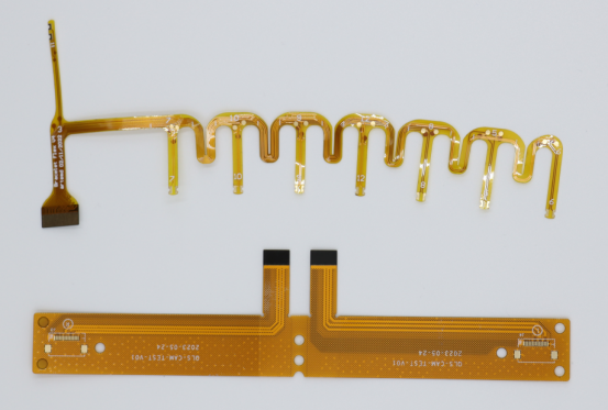
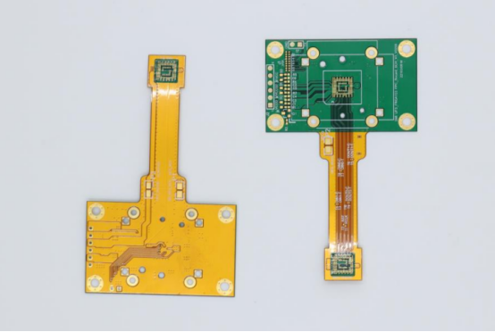
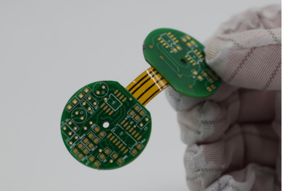
Flexible printed circuit boards (FPCs) are widely used in compact, high-density electronic devices such as smartphones, wearables, and automotive sensors. Their thin, bendable nature makes them particularly susceptible to EMI issues if not properly designed.
Effects on Device Performance and Reliability:
Uncontrolled EMI can cause signal distortion, timing errors, and even system failure. In high-speed flex circuits, interference may lead to data corruption or intermittent connectivity issues. For devices in critical applications, such as medical instruments or automotive electronics, these errors can have serious consequences.
Regulatory Standards and Industry Requirements:
Many regions have strict EMI regulations to protect electronic environments. The FCC in the United States and CE certification in Europe set limits for radiated and conducted emissions. Flex PCBs must comply with these standards to avoid legal and functional problems. Designing with EMI in mind from the start helps products pass compliance testing efficiently.
Impact on Neighboring Electronics:
Unshielded or poorly shielded flex circuits can emit electromagnetic noise that affects other nearby devices. For instance, a wearable sensor without proper EMI control could interfere with a smartphone’s wireless signals. Similarly, in automotive systems, unshielded FPCs can disrupt communication between electronic control units (ECUs). Proper EMI shielding in flex PCBs ensures that both the device itself and surrounding electronics operate without interference.
By understanding EMI and its implications, designers can create flex PCBs that are both high-performing and reliable, even in complex electronic environments.
Fundamentals of EMI Shielding
How EMI Shielding Works
EMI shielding protects electronic circuits by controlling unwanted electromagnetic energy. There are two main ways shielding works: absorption and reflection.
Absorption: The shield material absorbs electromagnetic waves, converting the energy into heat. This reduces the strength of the interference before it reaches sensitive components.
Reflection: The shield reflects electromagnetic waves away from the circuit, preventing them from entering or leaving the device. Metals such as copper, aluminum, and nickel are commonly used for reflection-based shielding because of their high conductivity.
The effectiveness of EMI shielding depends on both the material and its thickness. Thicker shields or those made of highly conductive materials generally provide better protection. However, in flexible PCBs, thickness must be balanced with mechanical flexibility. For example, a 22µm copper shield offers more EMI suppression than a 10µm layer, but it may reduce the bendability of the flex circuit. Designers must optimize this trade-off to ensure both electrical performance and mechanical reliability.
Types of EMI Shields for Flex Circuits
EMI shields for flex PCBs can be categorized based on placement and layer configuration:
Single-Sided Shields:
Placed on only one side of the flex circuit.
Pros: Low cost and minimal impact on flex thickness.
Cons: Limited shielding effectiveness, especially for high-speed or sensitive circuits.
Double-Sided Shields:
Covers both sides of the flex circuit.
Pros: Provides better EMI suppression than single-sided shields. Helps maintain signal integrity in high-speed traces.
Cons: Increases total flex thickness and may reduce bendability.
Multilayer Shields:
Integrated within multiple layers of the flex PCB.
Pros: Offers the highest EMI suppression and can be combined with controlled impedance designs for high-speed applications. Ideal for compact, sensitive electronics.
Cons: More complex to manufacture and increases cost and thickness.
Materials and Thickness:
Typical shielding materials include copper, aluminum, nickel, and conductive polymer composites.
Standard thicknesses range from 10µm to 22µm, with 22µm offering stronger EMI suppression but reducing flexibility.
Designers often select thinner layers for wearable or highly flexible devices and thicker layers for high-frequency, critical systems.
Choosing the Right Shield:
The choice between single-sided, double-sided, or multilayer EMI shields depends on:
Device sensitivity to interference
Required mechanical flexibility
Available PCB space and thickness constraints
Cost considerations
By understanding how shields absorb or reflect EMI and the trade-offs of different shield types, designers can make informed decisions to protect flex PCBs without compromising performance or reliability.
Design Challenges in EMI Shielding for Flex PCBs
Mechanical and Flexibility Constraints
Adding EMI shields to flexible PCBs inevitably affects the mechanical properties of the board. Shield materials, such as copper or nickel, increase the overall thickness of the flex circuit. For example, a single 22µm copper shield may seem thin, but in a compact multilayer FPC, it can reduce the board’s ability to bend freely.
This added thickness introduces risks of bending, delamination, and mechanical failure. Repeated flexing in wearable devices or foldable electronics can cause cracks in the shield or the PCB itself. Designers must carefully balance the shield thickness with the required flexibility, often opting for thinner layers or strategically placing shields only where necessary.
Electrical and Signal Integrity Concerns
EMI shields can also affect the electrical performance of flex circuits. One key issue is controlled impedance, which is critical for high-speed signals. Adding a conductive shield can alter the board’s characteristic impedance, potentially causing signal reflections, crosstalk, or timing errors.
Parasitic effects from vias, layer transitions, and shield placement further complicate signal integrity. For instance, vias in differential pairs can introduce unwanted capacitance and inductance, creating noise or reducing signal quality. In high-speed flex circuits, even small parasitic variations can lead to data corruption. Designers need to carefully plan trace routing, layer stack-up, and shield placement to minimize these electrical challenges.
Cost and Manufacturing Considerations
EMI shielding adds both material and process costs to flex PCBs. Using thicker shields, multilayer shields, or high-conductivity materials increases manufacturing complexity and budget. For example, double-sided or multilayer shielding may require additional lamination steps, precise alignment, and extra quality control.
Designers must weigh the trade-offs between performance, reliability, and cost. High-performance applications may justify thicker shields or complex multilayer designs, while consumer devices may prioritize flexibility and affordability over maximum EMI suppression. Strategic decisions in shield type, material, and placement allow designers to achieve reliable EMI control without unnecessary expense.
By understanding these mechanical, electrical, and cost-related challenges, engineers can design EMI shields for flex PCBs that protect sensitive circuits while maintaining flexibility, signal integrity, and budget constraints.
Best Practices for EMI Shield Design
Signal Routing and Separation
Proper signal routing is essential for minimizing EMI in flexible PCBs. Keep high-speed traces—such as clock or data lines—separate from low-speed signals to reduce interference. Similarly, analog signals should be routed away from digital lines, as digital switching noise can easily distort sensitive analog circuits.
For example, in a wearable device, placing analog sensor traces on a separate layer from high-speed processor signals can dramatically reduce noise pickup. Designers can also use physical separation or grounded barriers between signal groups to further isolate them.
Optimizing Return Paths
Return paths provide a path for current back to the source and are critical for EMI control. Keep return paths short and direct to reduce loop area, which lowers radiated emissions.
A well-designed ground plane can serve as a continuous return path, improving both signal integrity and shielding effectiveness. For instance, a high-speed differential signal routed over a solid ground plane will experience fewer reflections and lower EMI than one with fragmented or long return paths.
Differential Trace Routing
Differential pairs are commonly used for high-speed signals because they naturally cancel out noise. To maximize this advantage:
Route differential traces close together to improve coupling and reduce common-mode interference.
Avoid vias within differential pairs when possible, as vias add parasitic capacitance and inductance. If vias are necessary, use oval anti-pads shared by the pair to minimize parasitic effects.
This approach is especially important in multilayer flex PCBs used in compact electronics, where small parasitics can significantly degrade high-speed signals.
Board Geometry Considerations
Sharp right-angle bends can create localized capacitance changes, causing reflections and EMI issues. To prevent this:
Use 45° or rounded corners instead of 90° angles.
Maintain consistent trace width and spacing to preserve characteristic impedance throughout the flex PCB.
Consistent impedance ensures that high-speed signals are not distorted, reducing EMI risk and improving overall reliability.
Solder Mask and Shielding Openings
Solder mask design also impacts EMI control:
Maintain a minimum solder mask opening of 0.8mm for shielded areas.
Ensure that the solder mask is at least 0.2mm away from traces to prevent unintended capacitive coupling.
Proper solder mask layout helps prevent leakage of EMI and ensures that shielding remains effective without compromising signal integrity.
Layer Stack-Up Recommendations
The layer stack-up of a flex PCB is crucial for EMI management:
Use dual-layer or multilayer FPCs when single-sided shielding cannot provide sufficient EMI suppression.
Carefully balance mechanical flexibility with shielding needs. For example, in a wearable device, a thin dual-layer design may offer sufficient EMI protection while maintaining the necessary bend radius.
Multilayer designs are ideal for high-speed, high-density circuits where EMI control is critical, such as automotive sensors or medical devices.
By following these best practices, designers can create flex PCBs that minimize interference, maintain signal integrity, and remain mechanically reliable. Proper routing, grounding, trace geometry, solder mask, and layer planning work together to optimize EMI shielding effectiveness.
Practical Examples and Case Studies
High-Speed Signal Flex PCB Example
High-speed flex PCBs, such as those used in communication modules or data converters, require careful EMI management to maintain signal integrity. A step-by-step approach to minimizing EMI includes:
1. Trace Separation: Place high-speed differential pairs away from low-speed or analog signals to reduce crosstalk.
2. Controlled Impedance: Adjust trace width, spacing, and layer stack-up to maintain consistent characteristic impedance.
3. Shielding: Add thin copper shields (10–22µm) over high-speed traces, focusing on areas near sensitive components.
4. Return Path Optimization: Ensure short, continuous ground planes beneath critical traces to minimize loop area.
5. Vias and Transitions: Avoid unnecessary vias in high-speed traces, or use oval anti-pads to reduce parasitic capacitance.
By following these steps, designers can reduce radiated emissions, improve signal quality, and comply with EMI standards even in densely packed high-speed flex circuits.
Flexible Display or Wearable Device Example
Flexible displays and wearable devices often combine multiple sensors, screens, and communication modules within a compact form factor. EMI shielding in these applications typically requires multilayer flex PCBs.
Multilayer Shielding: Incorporates internal ground planes and conductive shields between layers to block interference from adjacent circuits.
Signal Isolation: Sensitive analog signals, such as biometric sensor outputs, are routed on isolated layers with shielding above and below.
Flexibility Consideration: Thinner shields are used in areas that require bending, while thicker shields protect high-frequency components that are stationary.
This approach ensures that wearable electronics maintain reliable operation without disturbing other nearby devices, such as smartphones or wireless earbuds.
Comparison: Single-Sided vs. Double-Sided EMI Shields
Effectiveness:
Single-sided shields provide basic EMI protection, suitable for low-speed or less sensitive circuits.
Double-sided shields significantly improve suppression, especially for high-speed or densely packed flex circuits.
Cost:
Single-sided shields are lower cost and simpler to manufacture.
Double-sided or multilayer shields increase material use, fabrication steps, and overall PCB cost.
Reliability:
Single-sided shields may not fully protect against interference in critical applications, potentially causing performance issues.
Double-sided shields enhance both signal integrity and mechanical reliability, particularly in high-density or multilayer designs.
Designers must weigh cost versus performance when selecting the shielding approach, considering both EMI suppression needs and mechanical flexibility requirements.
These examples demonstrate how EMI shielding strategies apply to real-world flex PCB designs, helping engineers make informed choices for high-speed, wearable, and sensitive electronics.
Testing and Validation
EMI/EMC Testing Methods
Testing is a critical step to ensure that flexible PCBs meet EMI and EMC requirements. Lab testing allows engineers to measure radiated and conducted emissions in controlled environments. Common methods include:
Near-field probes: Measure electromagnetic fields close to the PCB to identify localized sources of EMI. Useful for detecting problem areas in high-speed traces or sensitive analog circuits.
TEM (Transverse Electromagnetic) cells: Provide a controlled environment to evaluate EMI emissions and susceptibility. TEM cells are especially useful for small flex PCBs and prototypes.
In addition to physical testing, simulation tools can predict EMI behavior before manufacturing. Electromagnetic simulation software models signal propagation, crosstalk, and shielding effectiveness in flex circuits. By combining simulations with lab measurements, designers can detect potential EMI issues early and reduce costly redesigns.
Design Iteration Based on Test Results
Test results often highlight areas that require design adjustment. Iterative improvements may include:
1. Trace Routing Adjustments: Rerouting high-speed signals away from sensitive traces or increasing spacing between differential pairs to reduce crosstalk.
2. Shield Thickness Modifications: Increasing or decreasing copper or conductive polymer shield layers depending on EMI suppression performance and mechanical flexibility.
3. Layer Stack-Up Changes: Adding internal ground planes, modifying layer order, or switching from single-sided to double-sided shielding to improve EMI control.
For example, a wearable flex PCB may initially fail near-field testing due to high-frequency interference from a sensor line. Adjusting the trace routing and adding a thin internal shield could bring the design within regulatory limits without affecting flexibility.
Iterative testing ensures that the final flex PCB design not only meets EMI/EMC standards but also maintains signal integrity, mechanical reliability, and cost efficiency.
Conclusion
Effective EMI shielding in flexible PCBs requires balancing mechanical flexibility, signal integrity, and cost. Optimizing trace routing, layer planning, and shielding placement helps minimize interference while maintaining reliable high-speed performance.
Designers should focus on separating high- and low-speed signals, managing return paths, and using appropriate shield thicknesses to ensure both EMI control and board flexibility.
At PCBMASTER, we deliver high-performance rigid-flex and HDI flex PCBs in as little as seven days, with 6–20 layers and flexible sections down to 0.8mm, using premium materials for reliable, interference-free designs.
FAQs
How does flex PCB thickness affect EMI shielding performance?
Thicker flex PCBs can support stronger EMI shields, improving interference suppression. However, increased thickness reduces flexibility and may introduce mechanical stress, so designers must balance shielding effectiveness with bendability.
What is the difference between single-sided and double-sided EMI shields?
Single-sided shields cover only one layer of the flex PCB and provide basic EMI protection at lower cost. Double-sided shields cover both sides, offering stronger suppression and better signal integrity, but they increase board thickness and manufacturing complexity.
Can vias in differential pairs cause EMI problems?
Yes. Vias introduce parasitic capacitance and inductance, which can create reflections and degrade signal quality. Using oval anti-pads or minimizing vias in differential traces reduces EMI risks.
How to test EMI effectiveness in flexible circuits?
EMI performance can be tested using lab methods like near-field probes and TEM cells, as well as simulation tools that predict interference patterns. Iterative testing allows designers to adjust trace routing, shielding, or layer stack-up for optimal performance.
What are common mistakes in EMI shield design for high-speed flex PCBs?
Common errors include placing high- and low-speed traces too close, using single-sided shields for critical circuits, neglecting return path optimization, and failing to consider mechanical flexibility. These mistakes can lead to signal degradation, interference, and reliability issues.

