


Top Printed Circuit Board Hardware Tips to Enhance Your Electronics Projects
When it comes to electronics projects, the smallest components can make the biggest difference. A well-chosen printed circuit board hardware setup doesn’t just support your design—it can elevate performance, reliability, and even innovation. From subtle material choices to precise component placement, every decision shapes the final outcome. Understanding these nuances can transform a good project into a standout one, giving both hobbyists and professionals an edge in creating electronics that truly perform.
Introduction to Printed Circuit Board Hardware
What is Printed Circuit Board (PCB) Hardware?
Printed Circuit Board (PCB) hardware refers to the physical components and structures that make up a PCB, allowing electronic circuits to function. Key components of PCB hardware include:
Boards: The main substrate that supports all other components, usually made from materials like FR4 or Rogers for high-frequency applications.
Traces: Conductive paths etched onto the board that connect electronic components.
Vias: Small holes that allow electrical connections between different layers of a PCB.
Connectors: Hardware interfaces for connecting the PCB to other devices or circuits.
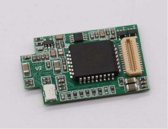
ICs (Integrated Circuits): Miniature electronic circuits that perform functions like processing, amplification, or memory storage.
Resistors and Capacitors: Basic electronic components that control current, voltage, and signal flow.
Unlike PCB design software tools, which help engineers plan layouts or simulate circuit behavior, PCB hardware refers to the actual physical elements that make the board work in real-world conditions. Simply put, hardware is “what you build with,” while software is “how you plan it.”
Importance of PCB Hardware in Electronics Projects
The quality and selection of PCB hardware directly impact the reliability, performance, and lifespan of any electronics project. High-quality components and proper layout can prevent failures such as signal interference, overheating, or mechanical stress.
Common pitfalls of neglecting hardware optimization include:
Poor signal integrity: Using substandard traces or vias can cause data loss or noise in high-speed circuits.
Mechanical failures: Inadequate connectors or poorly supported components may lead to broken boards or loose connections.
Thermal issues: Low-quality substrates or insufficient heat management can damage sensitive ICs.
Investing in reliable PCB hardware from the start saves time, reduces troubleshooting, and ensures the finished device performs as intended.
Overview of Common PCB Hardware Types
PCB hardware comes in several configurations, each suited to different applications:
Single-layer PCBs: Consist of a single conductive layer and are cost-effective for simple circuits like calculators or basic LED boards.
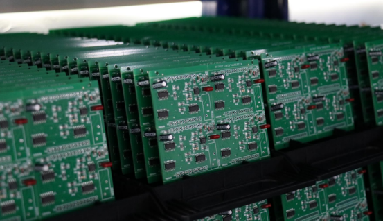
Multi-layer PCBs: Contain two or more conductive layers separated by insulating material. They are ideal for complex electronics like smartphones or industrial controllers, where space efficiency and signal integrity are critical.
Rigid PCBs: Standard boards that maintain their shape, commonly used in consumer electronics, computers, and automotive devices.
Flexible PCBs: Made with bendable substrates, they can be folded or twisted, perfect for wearable devices, medical sensors, or compact gadgets.
Rigid-flex PCBs: Combine rigid and flexible layers, offering mechanical stability and versatility in compact or high-density applications, such as aerospace electronics or foldable devices.
By understanding the types of PCB hardware, engineers can choose the right structure for their project’s technical requirements and physical constraints. For instance, a fitness tracker would benefit from a flexible PCB, while a desktop motherboard requires a rigid multi-layer design for high-performance circuits.
Selecting the Right PCB Hardware Components
Choosing High-Quality Materials
Selecting the right substrate material is one of the most critical decisions in PCB design. The most commonly used options include:
FR4: A widely used, cost-effective material made from woven fiberglass and epoxy resin. It provides good mechanical strength and electrical insulation for most standard electronics.
Rogers: A high-performance material designed for high-frequency or high-speed applications, offering superior thermal stability and lower signal loss compared to FR4.
Other materials: Polyimide, PTFE, and ceramic substrates are used in specialized applications like flexible electronics, RF circuits, or extreme thermal environments.
When choosing materials, engineers must balance cost versus performance. FR4 is affordable and sufficient for general electronics projects, while Rogers or ceramic substrates offer higher reliability and signal integrity for demanding applications but at a higher cost.
Example: For a basic LED controller, FR4 is sufficient. For a 5G communication module, a Rogers substrate may be required to handle high-frequency signals efficiently.
Components Compatibility
Proper hardware compatibility ensures smooth assembly and optimal circuit performance. Key considerations include:
IC Packages and Board Layout: Surface-mount devices (SMD) are smaller and suited for high-density, multi-layer PCBs, while through-hole components are easier to solder manually and provide stronger mechanical connections.
Connector Types and Pin Alignment: Ensure connectors match the mating components in size, pitch, and orientation. Misaligned pins or incorrect connector types can lead to signal loss, short circuits, or mechanical failure.
Step-by-step example:
1. Identify the IC package type (e.g., QFP, BGA, SOIC).
2. Check the PCB footprint matches the package dimensions.
3. Verify pin alignment for connectors relative to other components.
4. Test placement in a small prototype before full assembly.
Sourcing Reliable Components
Reliable sourcing is essential to avoid failures due to counterfeit or low-quality parts. Consider the following:
Trusted Suppliers and Certifications: Choose suppliers with certifications like RoHS (Restriction of Hazardous Substances) and IPC standards compliance. These ensure component quality, safety, and environmental compliance.
Avoiding Counterfeit Components: Purchase from authorized distributors, check datasheets carefully, and verify markings on ICs and passive components. Using counterfeit parts can lead to unpredictable failures, safety risks, and warranty issues.
Example: Major electronics manufacturers, such as Texas Instruments or Murata, provide authorized distributors lists. Cross-checking components against official datasheets ensures correct specifications.
PCB Design Tips to Optimize Hardware Performance
Layout and Trace Considerations
Proper PCB layout and trace design are crucial for signal integrity and overall performance. Key aspects include:
Trace Width and Spacing: Wider traces carry higher current with less resistance, while adequate spacing prevents short circuits and signal interference.
Impedance Control: Maintaining consistent trace impedance is essential for high-speed signals to avoid reflections and signal loss.
Step-by-step example of routing a high-speed signal:
1. Identify the signal type and required trace width for the current and frequency.
2. Keep traces as short and direct as possible to reduce delay and interference.
3. Maintain controlled impedance by calculating trace width and spacing relative to the PCB stack-up.
4. Avoid sharp 90-degree corners; use 45-degree bends or curves to reduce signal reflection.
5. Separate high-speed traces from noisy signals and power lines to minimize crosstalk.
Layer Stack-Up Planning
The number of layers in a PCB impacts signal quality, noise reduction, and overall design flexibility.
Multi-layer Boards: Adding layers allows for dedicated power and ground planes, reducing crosstalk and improving signal integrity.
4-layer vs. 6-layer Stack-Up:
- 4-layer boards: Typically include signal, ground, power, and another signal layer. Suitable for moderate complexity circuits.
- 6-layer boards: Add extra signal layers, improving routing flexibility and reducing interference for high-speed designs.
Example: A high-speed microcontroller board may use a 6-layer stack-up to separate digital and analog signals, minimizing noise and ensuring reliable performance.
Thermal Management Techniques
Managing heat is critical for PCB reliability, especially in high-power or densely packed designs. Key strategies include:
Heat Sinks: Attach to high-power ICs to dissipate heat away from the board.
Thermal Vias: Conduct heat from surface components to inner layers or the opposite side of the board.
Copper Pours and Planes: Large copper areas act as heat spreaders, reducing hot spots on the PCB.
Example of managing high-power ICs:
1. Identify ICs with high thermal dissipation requirements.
2. Place thermal vias directly beneath the IC pads to transfer heat to inner planes.
3. Connect copper pours to ground or power planes to further distribute heat.
4. Optionally, attach heat sinks or use thermal pads for additional cooling.
Assembly and Hardware Handling Best Practices
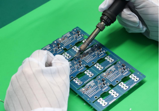
Soldering Techniques for PCB Hardware
Soldering is a fundamental step in assembling PCB hardware. Two common methods are:
Hand Soldering: Ideal for prototypes or small-volume projects. It provides flexibility but requires steady hands and careful temperature control.
Reflow Soldering: Typically used in mass production. Solder paste is applied, and the board passes through a controlled oven to melt the solder and attach components automatically.
Step-by-step hand soldering example:
1. Preheat the soldering iron to the recommended temperature (usually 350–400°C for lead-free solder).
2. Clean the component leads and PCB pads to remove oxidation.
3. Apply solder to the heated pad while touching the component lead.
4. Remove the iron and let the solder solidify naturally.
5. Inspect for cold joints or solder bridges.
Common mistakes to avoid:
Overheating components, which can damage ICs.
Using too much solder, causing short circuits.
Not cleaning flux residues, which may corrode traces over time.
Preventing Physical Damage
PCB hardware is sensitive to static electricity, mechanical stress, and improper storage. Key precautions include:
ESD Protection: Use anti-static wrist straps, mats, and bags to prevent electrostatic discharge from damaging sensitive ICs.
Proper Handling Tools: Use tweezers, vacuum pickup tools, and precision pliers to avoid bending pins or scratching the board.
Storage Tips: Store boards in anti-static containers and avoid stacking heavy items on top.
Example of hardware failure due to mishandling:
A microcontroller destroyed by ESD when handled without grounding.
Broken connector pins caused by using pliers instead of precision tools.
Warped PCB due to stacking multiple boards under weight.
Inspection and Testing
Inspection and testing ensure that PCB hardware functions correctly before deployment. Common tools and techniques include:
Multimeters: Measure voltage, current, and resistance to check connectivity.
Oscilloscopes: Observe signal quality and timing in high-speed circuits.
Automated Optical Inspection (AOI): Detect soldering defects, missing components, or misalignments automatically.
Step-by-step testing workflow for new boards:
1. Visually inspect for solder bridges, misaligned components, and damaged traces.
2. Use a multimeter to check continuity on all critical paths.
3. Power up the board gradually and monitor voltage levels.
4. Verify signals with an oscilloscope for expected timing and waveform integrity.
5. Use AOI for comprehensive inspection in larger or complex boards.
Enhancing Project Reliability with Hardware Optimization
Reducing Signal Interference and Noise
Signal interference and electrical noise can degrade PCB performance, especially in high-speed circuits. Effective strategies include:
Shielding Techniques: Use metal shields, grounded enclosures, or copper pours around sensitive components to block electromagnetic interference (EMI).
Grounding Strategies: Implement a solid ground plane, separate analog and digital grounds, and use proper via placement to reduce noise coupling.
Comparison Example:
Poor Layout: High-speed traces routed near noisy power lines, no shielding, resulting in data errors or signal distortion.
Optimized Layout: Traces separated from noise sources, grounded shields applied, and controlled impedance maintained, leading to stable signal transmission.
Ensuring Mechanical Stability
Mechanical support is essential to prevent physical damage and maintain reliable operation. Key considerations include:
Mounting Methods: Use standoffs, screws, and brackets to secure the PCB within enclosures.
Enclosures: Protect boards from dust, moisture, and mechanical shocks.
Vibration Resistance: Design with flexible mounts or shock-absorbing materials in environments prone to vibrations.
Example of hardware failure due to poor support:
A PCB in an automotive module cracked due to vibration stress.
Connectors loosened in a consumer device because the board was not properly mounted.
Sensitive components shifted inside an industrial sensor, causing intermittent failures.
Lifecycle and Maintenance Tips
Regular maintenance ensures PCB hardware continues to function reliably over time. Recommended practices include:
Cleaning: Remove dust, flux residues, and corrosion with appropriate cleaning solutions.
Inspection: Periodically check solder joints, connectors, and critical components for signs of wear or damage.
Component Replacement: Replace aged capacitors, resistors, or ICs before they fail to prevent cascading issues.
Example of preventive maintenance improving longevity:
Cleaning and inspecting a power supply PCB every six months reduced unexpected failures by 40%.
Replacing electrolytic capacitors in older audio equipment prevented performance degradation and extended device life.
Advanced PCB Hardware Tips for Electronics Enthusiasts
Utilizing High-Speed and High-Density Interconnects
High-speed and high-density interconnects (HDI) allow designers to pack more functionality into smaller boards without sacrificing performance. Key concepts include:
HDI (High-Density Interconnect): Uses finer traces, smaller vias, and closer component placement for compact, high-performance PCBs.
Blind/Buried Vias: Blind vias connect outer layers to inner layers without passing through the entire board. Buried vias connect only internal layers. These help save space and reduce routing complexity.
Microvias: Extremely small vias, often laser-drilled, used for very high-density designs.
Step-by-step example of implementing HDI:
Identify high-density sections requiring more routing space.
Replace through-hole vias with microvias where possible.
Separate power and ground planes for signal integrity.
Use fine-pitch components to reduce board footprint.
Simulate signal paths to ensure minimal interference.
Integrating Modular Hardware Components
Modular PCB designs break a system into reusable, standardized blocks. This approach has distinct advantages and trade-offs:
Pros:
Faster prototyping and assembly.
Easier upgrades or replacements of individual modules.
Reduced development risk for complex projects.
Cons:
Slightly larger overall footprint compared to fully custom designs.
Extra connectors may introduce small signal losses or mechanical complexity.
Case study example:
An IoT sensor hub used a modular design where the communication, power, and sensing modules were separate PCBs. This allowed quick swapping of modules for upgrades without redesigning the entire system.
Future Trends in PCB Hardware
PCB hardware continues to evolve with technology and user demands. Key emerging trends include:
Flexible and Wearable PCBs: Bendable or stretchable boards for smart wearables, medical sensors, and foldable electronics.
AI-Driven PCB Design Tools: Software that uses artificial intelligence to optimize layouts, component placement, and routing automatically.
Emerging Materials: Advanced substrates such as polyimide, ceramic, and graphene composites offer improved thermal performance, signal integrity, and mechanical flexibility.
Comparison example:
Flexible PCBs: Ideal for wearable devices due to bending tolerance but can be more expensive and delicate.
Ceramic PCBs: Excellent for high-frequency or high-power applications but rigid and heavier.
These innovations allow electronics enthusiasts and professionals to create more compact, efficient, and durable devices than ever before.
Conclusion
Optimizing PCB hardware is essential for building reliable, high-performance electronics. From selecting quality materials and compatible components to careful layout, thermal management, and proper assembly, each step contributes to the success of your project. Applying shielding techniques, ensuring mechanical stability, and performing regular inspection further enhance durability and signal integrity.
Experimentation and iterative testing are key to continuous improvement. Prototyping, monitoring performance, and making incremental adjustments help refine designs and prevent common failures. Whether exploring high-density interconnects, modular components, or flexible PCB materials, a hands-on, methodical approach allows electronics enthusiasts and professionals to achieve optimal results.
If you have any questions or want to learn more about PCB and PCBA solutions, PCBMASTER is ready to provide expert guidance. As an experienced PCB and PCBA manufacturer, we can help you select the right materials, components, and processes to make your electronics projects successful.
FAQs
What are the most common mistakes in PCB hardware selection?
Common mistakes include choosing low-quality components to save costs, ignoring compatibility between IC packages and board layout, and selecting inappropriate substrates for the project’s thermal or signal requirements. Other errors include neglecting connector types, pin alignment, or failing to verify supplier reliability, which can lead to performance issues or premature hardware failure.
How do I choose between single-layer and multi-layer PCBs for my project?
Single-layer PCBs are simple, cost-effective, and suitable for basic circuits with minimal components, such as LED drivers or simple controllers. Multi-layer PCBs provide extra layers for signal routing, power, and ground planes, making them ideal for high-speed, high-density, or complex projects like smartphones, industrial controllers, and IoT devices. The choice depends on circuit complexity, space constraints, and performance requirements.
What are the best practices for soldering sensitive PCB components?
For sensitive components, always use proper temperature control and avoid overheating. Hand soldering works well for prototypes, while reflow soldering is preferred for mass production. Steps include cleaning pads and component leads, applying solder carefully, and inspecting joints for cold solder or bridges. Additionally, always use ESD protection to prevent electrostatic damage.
How can I reduce electronic noise in high-speed PCB designs?
Reducing noise involves proper layout and grounding strategies. Use solid ground planes, separate analog and digital signals, and implement shielding around sensitive traces. Controlled impedance traces, careful routing, and avoiding long parallel runs of high-speed signals also help. Adding decoupling capacitors near ICs and using differential pairs for critical signals further improves signal integrity.
Which materials provide the best thermal management for PCBs?
Materials like Rogers, ceramic, and high-grade polyimide substrates excel at thermal management, offering better heat dissipation than standard FR4. Additionally, design techniques such as copper pours, thermal vias, and heat sinks enhance cooling for high-power ICs. The material choice depends on the project’s operating temperature, power density, and performance requirements.

