


Solving BGA Soldering Problems: Design Flaws, Process Defects, and Proven Fixes
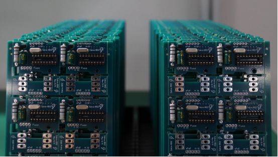
In modern electronics manufacturing, BGA soldering remains one of the most demanding yet critical processes. Hidden beneath the chip package, hundreds or even thousands of tiny solder balls form the only electrical and mechanical link between device and board. A small design flaw or temperature deviation can silently compromise connection quality, leading to failures that are hard to detect and costly to fix. Achieving stable, defect-free joints requires precision at every stage—from pad design to reflow control—where even the smallest oversight can determine the difference between reliability and rework.
Why BGA Soldering Is Challenging
The Hidden Nature of BGA Joints
One of the biggest challenges in BGA soldering is that the joints are completely hidden beneath the package. Unlike traditional leaded components, where solder fillets are visible for inspection, every BGA connection is made underneath the chip through tiny solder balls. Once the component is mounted, these joints are invisible to the naked eye and cannot be checked by standard optical inspection.
Because of this concealed structure, defects such as voids, opens, bridging, or head-in-pillow (HIP) can occur without immediate detection. Manufacturers rely on advanced X-ray inspection or CT scanning to evaluate solder joint quality. However, these methods are time-consuming and costly, making prevention through proper design and process control far more efficient.
Design accuracy plays a critical role here. If pad sizes, solder mask openings, or via placements are even slightly off, the solder balls may not align perfectly during reflow. Inaccurate alignment can lead to weak connections or intermittent electrical contact. Likewise, the reflow temperature profile must be tightly controlled — too low and the solder may not wet properly; too high and the balls can collapse or bridge. For reliable BGA joints, precision in both design and temperature management is not optional; it’s essential.
Factors Affecting BGA Solder Quality
BGA solder quality depends on the combined influence of PCB design, pad geometry, via processing, and reflow profile. These factors are interconnected, and even minor inconsistencies can significantly affect assembly yield.
For example, pad geometry determines how the molten solder ball spreads and bonds. If the pad is too small, the joint may not form a complete connection; if too large, solder can overflow and cause bridging. Similarly, via processing—whether the vias under BGA pads are open, tented, or resin-filled—directly impacts solder reliability. Open vias can draw solder away during reflow, creating voids or incomplete joints.
The layout design also affects heat distribution during reflow. Dense copper areas or uneven thermal masses can cause temperature imbalances, leading to inconsistent melting across the BGA array. A precisely tuned reflow profile helps maintain uniform heating, minimizing issues like voids or head-in-pillow defects.
In practice, a few microns of misalignment or a few degrees of temperature difference can reduce yield dramatically. That’s why successful BGA soldering requires both a robust design foundation and a stable, repeatable reflow process. When these parameters are properly aligned, manufacturers achieve stronger joints, higher yields, and longer product lifespans.
Common BGA Soldering Defects and Their Root Causes
Solder Ball Voids and Incomplete Wetting
Voids are small air pockets or gas bubbles trapped within a solder joint. In BGA soldering, voids form when flux gases or moisture cannot escape during reflow, or when reflow heating is uneven across the board. Contaminated pads, oxidized surfaces, or excessive flux residue can further prevent the solder from wetting properly.
Incomplete wetting occurs when the solder fails to spread evenly over the pad, creating weak or unreliable connections. One common cause is excessive via exposure under the pad — open vias allow molten solder to wick away from the joint, reducing the solder volume and forming cavities. Poor paste printing is another contributor; inconsistent paste thickness can cause uneven reflow behavior and air entrapment.
To minimize voiding, manufacturers should ensure clean pad surfaces, uniform paste application, and controlled reflow heating. Using resin-filled vias or via-in-pad designs can prevent solder from escaping through holes, ensuring consistent joint formation and stronger mechanical integrity.
Solder Bridging and Shorts
Solder bridging happens when two adjacent BGA pads unintentionally connect through excess solder, forming a short circuit. This often results from improper pad spacing, excess solder paste, or misaligned stencil apertures during printing. In fine-pitch BGAs, even a 1–2 mil deviation in pad distance can increase the risk of bridging.
The stencil design directly affects solder volume and distribution. Overly large stencil openings or improper thickness allow too much paste to be deposited, which then flows together during reflow. High reflow temperatures or low surface tension can worsen this effect, especially in densely packed BGAs.
To prevent bridging, engineers should optimize stencil design, control paste deposition volume, and ensure sufficient pad-to-pad clearance. Adjusting the aperture ratio (typically 1:1 or slightly reduced to pad size) helps maintain the right solder volume. Automated inspection after paste printing can detect bridging risks before components are placed, reducing costly rework later.
Head-in-Pillow (HIP) and Open Joints
Head-in-Pillow (HIP) is a distinctive BGA defect where the solder ball and paste appear to touch but do not fully fuse. Under X-ray inspection, it resembles two separate hemispheres — like a “head on a pillow.” This defect occurs when oxidation, contamination, or warpage prevents proper wetting during reflow.
During heating, the PCB and component package expand at different rates. If the board warps, some solder balls lift off the pads temporarily. When cooling begins, the parts may realign physically but fail to form a metallurgical bond, leaving an open joint.
Preventing HIP requires tight control of coplanarity and surface cleanliness. Using nitrogen reflow atmospheres minimizes oxidation, while adjusting soak time and ramp rate ensures the solder remains molten long enough to complete wetting. Proper moisture control in storage and pre-bake procedures can also prevent oxidation-related defects.
Solder Ball Collapse or Misalignment
Solder ball collapse occurs when the solder balls flatten excessively during reflow, often due to overheating or excessive time above liquidus temperature. When the solder remains molten for too long, surface tension weakens, causing the ball to lose its defined shape and spread too far. This can lead to bridging or mechanical stress.
Misalignment, on the other hand, happens when the BGA component shifts during placement or early in the reflow process. Uneven PCB warpage or vibration in the reflow oven can also distort solder ball positioning. Inaccurate placement systems, especially when handling ultra-fine pitch BGAs, further increase the risk.
To avoid these problems, maintain precise temperature control, especially in the preheat and soak zones, and use a flat, rigid PCB structure to reduce warpage. High-accuracy placement machines with closed-loop vision systems are essential for fine-pitch alignment. A stable reflow profile and proper support fixtures can ensure each solder ball retains its shape and position, resulting in consistent and reliable joints.
Design-Level Causes of BGA Soldering Problems
Untreated or Open Vias Under Pads
One of the most common design-level causes of BGA soldering failure is the use of unfilled or open vias directly beneath solder pads. When vias are left untreated, molten solder can wick through the via hole during reflow, draining solder away from the joint area — a problem known as solder starvation. This results in weak mechanical strength and poor electrical connectivity, especially in fine-pitch BGAs where solder volume is already limited.
The solution is to seal via holes using resin plugging or copper filling. These methods block the solder from flowing into the via, preserving the correct solder volume on the pad surface. For high-reliability applications such as aerospace or high-speed networking, via-in-pad with copper filling and planarization ensures both thermal stability and uniform solder joint height. Designers should always check that the via process matches the assembly requirements before fabrication to prevent hidden joint defects.
Uneven Pad Sizes and Inaccurate Mask Openings
Even small variations in pad diameter or solder mask opening size can significantly affect solder joint consistency. When pad sizes are uneven, solder paste volume distribution becomes irregular, leading to overfilled or underfilled joints. Larger pads attract more solder, while smaller ones starve — creating stress concentration points that can crack during thermal cycling.
A best practice is to maintain a consistent pad-to-ball diameter ratio within ±20%, ensuring balanced wetting across all connections. Inaccurate solder mask openings can also alter solder volume by restricting paste flow or allowing overflow. To achieve uniformity, designers should use precise solder mask-defined (SMD) or non-solder mask-defined (NSMD) pad designs depending on reliability needs — NSMD pads are preferred for most BGAs because they promote better solder fillet formation.
Inadequate Trace Escape and Routing Choices
As BGAs evolve toward finer pitches (0.8 mm, 0.5 mm, or smaller), trace routing between pads becomes increasingly challenging. When designers attempt to run traces between pads at less than 10 mil pitch, they risk insufficient clearance, which can cause solder bridging or mask misalignment. Additionally, narrow traces and vias too close to pads can disturb solder flow during reflow, resulting in opens or voids.
To manage dense interconnections effectively, use dog-bone escape routing, where a short trace connects the pad to a via outside the BGA area. For ultra-fine pitch designs, via-in-pad microvias are a more reliable choice — they save space and maintain signal integrity while reducing the chance of solder wicking. Optimized escape routing ensures cleaner solder joints, predictable impedance, and easier assembly with automated placement systems.
Overlapping Solder Mask or Improper Window Design
Solder mask design plays a critical role in preventing short circuits, solder bridging, and exposed copper. If the solder mask overlaps a BGA pad or the mask opening (window) is misaligned, molten solder may spread unevenly, leaving exposed copper traces or bridging between adjacent pads. This often occurs when mask registration tolerances are too tight for the board’s pitch size.
For fine-pitch BGAs, the general guideline is to provide solder mask clearance of 3–5 mils (0.075–0.125 mm) around each pad. This ensures that the mask does not interfere with solder wetting while still protecting nearby copper features. When designing high-density layouts, using solder mask-defined pads can improve alignment precision, but the process must be tightly controlled to avoid reduced solderable areas. Consistent solder mask design and accurate registration are essential to maintaining BGA reliability and long-term electrical performance.
Process Optimization for Reliable BGA Assembly
Solder Paste Printing Control
Solder paste printing is a critical step in BGA assembly because it determines how much solder is available for each joint. Factors such as stencil thickness, aperture shape, and paste viscosity directly affect paste deposition. For instance, thicker stencils deposit more solder, while smaller apertures may restrict flow and create insufficient solder volume.
Uniform paste deposition reduces solder bridging, voids, and open joints. When the paste layer is even across all pads, molten solder melts consistently during reflow, forming strong mechanical and electrical connections. Using proper stencil design — including step-down apertures for fine-pitch BGAs — and controlling paste rheology ensures repeatable printing and higher yield.
Component Placement Accuracy
Accurate placement of BGA components is essential because misalignment or tilting can lead to defects during reflow. High-speed placement machines are ideal for mass production of small components like resistors and capacitors, but their tolerances may not be sufficient for fine-pitch BGAs. Precision placement machines, with closed-loop vision systems, offer higher accuracy for large or sensitive ICs.
Strategies to prevent offset or tilting include proper PCB support during placement, verifying coplanarity of component leads, and calibrating placement nozzles. For example, a slight tilt in a 0.5 mm pitch BGA can result in bridging or head-in-pillow defects, highlighting the importance of machine precision and board flatness.
Reflow Temperature Profile Tuning
The reflow oven profile is a key factor in forming reliable BGA solder joints. Reflow typically consists of four stages:
1. Preheat – Gradually warms the board to activate flux and prevent thermal shock.
2. Soak – Ensures uniform temperature across the PCB and stabilizes the solder paste.
3. Reflow – Melts the solder balls and paste to form metallurgical bonds.
4. Cooling – Solidifies the solder, establishing mechanical strength and electrical continuity.
Ramp rate and peak temperature are crucial. Too rapid a ramp can cause voids or component shift, while excessive peak temperature may lead to solder collapse or thermal damage. Controlled heating ensures consistent wetting and joint formation across all pads.
Inspection and Verification
Because BGA joints are hidden, inspection is essential to verify quality. X-ray inspection (X-ray AOI) allows detection of internal voids, open joints, misaligned balls, and bridging. 3D AOI provides additional height and volume information to ensure proper solder fillets.
For example, an acceptable joint shows uniform solder coverage with minimal voiding (typically <10% of ball volume), while a defective joint may exhibit voids exceeding 25%, incomplete wetting, or misaligned balls. Implementing thorough inspection not only identifies defects before final assembly but also provides feedback for process optimization, including paste volume adjustment, placement accuracy, or reflow profile tuning.
Preventive Design and Manufacturing Strategies
Use Resin-Filled or Plugged Vias in BGA Regions
Resin-filled or plugged vias are a key design strategy for improving solder joint reliability and pad planarity in BGA assemblies. Open vias under pads can cause solder wicking, reducing the effective solder volume and creating weak or incomplete joints. Filling the via with resin or copper ensures a flat, stable pad surface, which helps the solder ball maintain its shape and wet the pad evenly during reflow.
For example, in fine-pitch BGAs (≤0.5 mm), using resin-filled vias reduces void formation and prevents head-in-pillow defects, enhancing both mechanical strength and long-term electrical performance. Designers should specify the via filling method during PCB layout to ensure the assembly process achieves high yield.
Match Pad and Ball Dimensions Early in Layout
The ratio between BGA pad size and solder ball diameter is critical for both mechanical and electrical performance. Pads that are too large can lead to solder spreading or bridging, while pads that are too small can cause incomplete wetting or weak joints.
Maintaining the correct pad-to-ball ratio, typically within ±20% of the nominal ball diameter, ensures consistent solder volume and proper metallurgical bonding. Early layout consideration allows engineers to balance signal integrity, thermal dissipation, and mechanical robustness without requiring costly design adjustments later.
Review Thermal Profiles and Stencil Designs Together
Cross-functional review of reflow thermal profiles and stencil designs is essential for preventing yield-limiting defects. The stencil determines paste volume, while the reflow profile controls melting and wetting behavior. If paste thickness or aperture size is mismatched with the oven profile, issues such as voids, solder ball collapse, or bridging can occur.
A practical approach is to perform DFM (Design for Manufacturability) reviews that involve both layout and process engineers. By simulating paste deposition and thermal behavior together, teams can detect potential problem areas before production, optimizing both assembly reliability and first-pass yield.
Document Design Rules for BGA-Specific Fabrication
Maintaining internal design rules and checklists for BGA fabrication ensures consistency and reduces errors. Key items include pad dimensions, solder mask clearance, via types (filled, plugged, or tented), and trace escape routing. Documenting these standards enables design engineers to follow best practices and preemptively address common soldering problems.
For example, a well-maintained BGA design rule checklist helps prevent issues like misaligned pads, insufficient solder mask clearance, or improperly sized vias, all of which can reduce reliability or cause rework. Over time, this structured approach builds a knowledge base that streamlines future BGA designs and supports high-yield manufacturing.
Summary and Key Takeaways
Most BGA soldering defects trace back to early design decisions, including pad size, via treatment, trace routing, and solder mask alignment. A small miscalculation at the layout stage can lead to voids, bridging, or head-in-pillow defects during assembly. This highlights the importance of strong collaboration between PCB layout engineers and SMT process teams, ensuring that design choices align with manufacturing capabilities and yield requirements.
Conducting early DFM validation and reflow simulation for complex BGA packages can identify potential issues before production, reducing costly rework and improving first-pass yield. By simulating solder flow, thermal profiles, and component placement, teams can proactively optimize the PCB design for reliable assembly.
At PCBMASTER, we emphasize that reliable BGA assembly doesn’t start on the production line—it starts in design. Prioritizing manufacturability, adhering to proven design rules, and integrating process-aware simulations ensures that every BGA joint is strong, consistent, and defect-free, delivering high-performance and long-lasting PCB assemblies.
FAQs
What causes voids in BGA solder joints and how can they be reduced?
Voids are small air pockets trapped inside solder joints. They are usually caused by trapped flux gases, moisture, or uneven heating during reflow. Contaminated pads or open vias under the BGA can worsen void formation. To reduce voids, manufacturers can use resin-filled or plugged vias, ensure clean pad surfaces, maintain uniform solder paste deposition, and apply a controlled reflow temperature profile that allows gases to escape before solder solidifies.
How do via-in-pad designs affect BGA solder reliability?
Via-in-pad designs place vias directly under BGA pads. If left open, they can wick solder away, causing weak or incomplete joints. Using resin-filled or copper-plugged vias ensures solder remains on the pad, improving mechanical strength and electrical reliability. Proper via treatment also maintains planarity, helping the solder balls form consistent, defect-free joints.
What is the ideal reflow profile for lead-free BGA soldering?
A lead-free reflow profile typically includes four stages:
1. Preheat: Gradually warms the PCB to prevent thermal shock and activate flux.
2. Soak: Stabilizes temperature across the board and ensures uniform heating.
3. Reflow: Melts solder balls and paste to form metallurgical bonds.
4. Cooling: Solidifies the solder, forming strong mechanical and electrical connections.
Key parameters include controlled ramp rate, sufficient soak time, and proper peak temperature to prevent voids, solder collapse, or bridging. Lead-free solder generally requires higher peak temperatures than SnPb solder, so careful tuning is essential.
Why does head-in-pillow occur and how can it be prevented?
Head-in-pillow (HIP) is a defect where the solder ball and paste touch but fail to fuse, leaving an incomplete joint. It occurs due to oxidation, contamination, or warpage, which prevents proper wetting during reflow. Prevention strategies include ensuring coplanarity of components and PCB, using a nitrogen reflow atmosphere to reduce oxidation, and adjusting soak and ramp times to allow full solder fusion. Proper moisture control and pre-baking components can also help.
How can X-ray inspection help identify hidden BGA defects?
Since BGA solder joints are hidden beneath the package, X-ray inspection is the only non-destructive method to detect internal defects. It can identify voids, open joints, solder bridging, misalignment, and head-in-pillow defects. 3D X-ray or X-ray AOI provides volume and alignment information, helping manufacturers verify joint quality, optimize reflow processes, and catch defects before final assembly, reducing rework and improving yield.

