


Etched FPC: Complete Guide to Design, Fabrication, and Applications
In the world of modern electronics, flexibility and precision are no longer optional—they’re essential. Etched flexible printed circuits (FPCs) have emerged as the silent backbone behind sleek smartphones, wearable devices, and advanced automotive systems, enabling complex connections in spaces where rigid boards simply can’t fit. With their ability to combine durability, miniaturization, and high-performance signal routing, etched FPCs are reshaping how engineers approach design and innovation. Understanding their potential opens the door to smarter, more efficient, and more compact electronic solutions.
Introduction to Etched FPC
What is an Etched FPC?
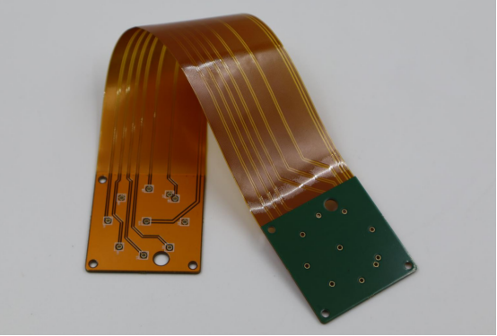
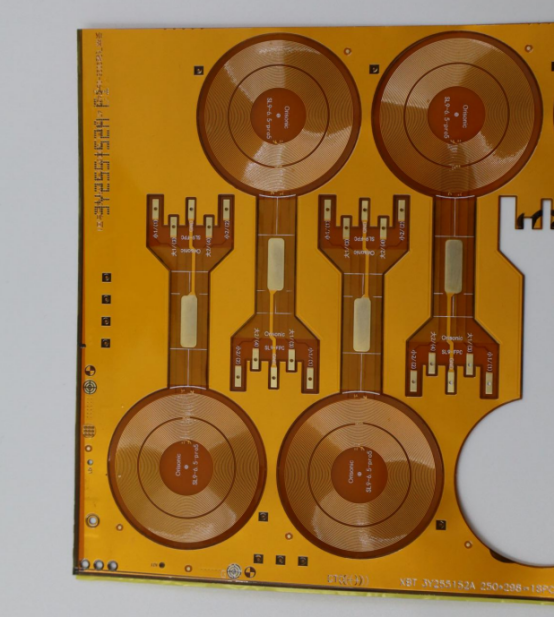
An etched flexible printed circuit (FPC) is a type of flexible circuit board where the conductive pathways are formed by removing excess copper from a copper-clad flexible substrate. Unlike additive methods, where copper is deposited to form circuits, the etching process is subtractive: it starts with a solid copper layer and carefully removes the unwanted areas to create precise circuit patterns.
The basic structure of an etched FPC typically includes:
A flexible substrate, usually polyimide or polyester, which provides mechanical support and bendability.
Copper traces, which are etched to form electrical connections.
Protective layers, such as coverlays or solder masks, to shield the circuits from moisture and mechanical stress.
Compared to traditional FPCs made with additive processes, etched FPCs offer higher precision and finer feature sizes, making them ideal for high-density and miniaturized electronic designs. For example, devices requiring ultra-thin circuits, such as foldable smartphones, rely on etched FPCs to maintain both flexibility and reliable electrical performance.
Why Etched FPCs Are Important
Etched FPCs play a critical role in modern electronics because they combine flexibility, durability, and electrical performance in a compact form factor. Some of their key advantages include:
Miniaturization: Fine etched traces allow designers to pack more circuits into a smaller area.
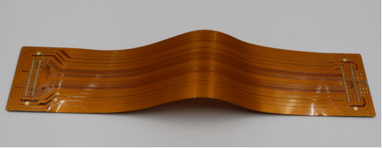
Flexibility: Etched FPCs can bend, fold, or twist without damaging the electrical pathways, enabling designs that rigid PCBs cannot support.
Signal Integrity: Precise copper etching reduces interference and maintains consistent electrical performance, even at high frequencies.
These characteristics make etched FPCs widely used across multiple industries:
Consumer electronics: Smartphones, tablets, wearable devices, and laptops use etched FPCs for compact and reliable internal connections.
Automotive electronics: Dashboard displays, sensors, and infotainment systems require flexible circuits that can withstand vibrations and temperature variations.
Medical devices: Wearable monitors, implantable sensors, and diagnostic equipment benefit from thin, reliable, and highly flexible circuit designs.
By providing both mechanical adaptability and electrical precision, etched FPCs enable innovations in devices where space is limited, reliability is critical, and performance cannot be compromised.
Etched FPC Design Principles
Materials Selection
Choosing the right materials is the foundation of a reliable etched FPC. The flexible substrate provides mechanical support and determines how much the circuit can bend or twist. The most common substrates are:
Polyimide (PI): Offers excellent thermal stability, chemical resistance, and mechanical strength. Ideal for high-temperature applications and high-density circuits.
Polyester (PET): Less expensive than polyimide, suitable for simpler circuits with moderate thermal requirements.
The type of copper used also affects performance:
Rolled Annealed (RA) Copper: Soft, highly flexible, and ideal for circuits that need frequent bending or folding.
Electrodeposited (ED) Copper: Harder and less flexible but offers better dimensional stability for fine-pitch designs.
Selecting the right combination of substrate and copper ensures mechanical durability, electrical reliability, and manufacturability.
Circuit Layout and Trace Design
Proper circuit layout is essential for both functionality and durability. Key considerations include:
Minimum trace width and spacing: Determines the electrical capacity and reduces the risk of short circuits. For high-density designs, widths as narrow as 3–5 mils are achievable with modern etching processes.
High-frequency signal routing: Controlled impedance and minimal crosstalk are critical. Techniques such as differential pair routing and careful grounding help maintain signal integrity.
Example of layout optimization: In a wearable device, traces near a bending edge should follow smooth curves rather than sharp corners. This prevents stress concentrations that could lead to cracking. Designers may also stagger traces across layers to distribute mechanical stress evenly.
Layer Stack-Up and Thickness
The number of layers and total thickness directly influence flexibility, thermal performance, and signal integrity:
Single-layer etched FPCs: Thinner, more flexible, suitable for simple connections where space is limited.
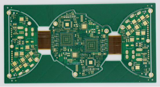
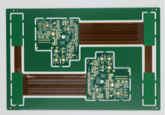
Multi-layer etched FPCs: Allow complex interconnections and high-density circuits but reduce bendability. Designers must balance the number of layers with the required flexibility.
Effect on performance: Increasing thickness improves thermal dissipation and mechanical strength but may introduce signal delay in high-frequency circuits. Optimizing layer stack-up ensures reliability while maintaining performance.
Design Rules for Manufacturability
Design rules ensure that an etched FPC can be manufactured accurately and efficiently. A DRF (Design Rule for Fabrication) provides clear guidelines for trace width, spacing, via size, and layer alignment.
Step-by-step guide from schematic to fabrication:
1. Start with the circuit schematic and define all electrical connections.
2. Translate the schematic into a PCB layout, considering trace routing, bend areas, and layer stack-up.
3. Apply DRF checks to confirm that all traces, vias, and pads meet minimum fabrication limits.
4. Generate fabrication files (Gerber, NC drill, and assembly drawings) ready for production.
5. Review with the manufacturer to ensure compliance with equipment capabilities and tolerances.
Following these principles ensures a high-quality, reliable, and manufacturable etched FPC, reducing errors during fabrication and improving overall product performance.
Fabrication Process of Etched FPC
Overview of Subtractive Etching Process
The subtractive etching process is the core method used to manufacture etched FPCs. It removes unwanted copper from a flexible substrate to create precise circuit patterns. The process typically involves four main steps:
1. Surface Preparation and Cleaning
The copper-clad flexible substrate is thoroughly cleaned to remove dust, oils, and oxidation.
A clean surface ensures strong adhesion of the photoresist and prevents defects during etching.
2. Photoresist Application and UV Exposure
A photosensitive resist is applied evenly over the copper layer.
The circuit pattern is transferred using UV light exposure through a photomask.
Exposed areas of the photoresist harden, protecting the underlying copper.
3. Development and Etching of Copper
The unhardened photoresist is removed, exposing the copper that needs to be etched away.
A chemical etchant selectively removes the exposed copper, leaving behind the desired circuit traces.
Step-by-step etching control ensures accurate trace width and spacing, critical for high-density circuits.
4. Photoresist Removal and Inspection
The remaining photoresist is stripped, revealing clean copper traces.
Initial inspections verify pattern accuracy and detect defects before surface finishing.
Surface Finishing and Treatments
After etching, surface finishes are applied to protect copper, improve solderability, and enhance reliability. Common finishes include:
ENIG (Electroless Nickel Immersion Gold): Provides excellent corrosion resistance and flat solderable surfaces; ideal for high-reliability applications.
OSP (Organic Solderability Preservative): Environmentally friendly, cost-effective, and suitable for short-term storage and simple soldering.
Immersion Tin: Good solderability and flat surface, often used for lead-free assembly.
Choosing the right finish depends on application requirements, assembly processes, and long-term reliability.
Quality Control and Testing
Quality assurance is critical in etched FPC fabrication to ensure durability and electrical performance. Typical QC and testing methods include:
Visual Inspection: Identifies visible defects like scratches, misalignments, or incomplete etching.
AOI (Automated Optical Inspection): Detects trace width deviations, missing copper, and micro-defects automatically.
Electrical Testing: Confirms continuity, correct connections, and controlled impedance for high-frequency circuits.
Mechanical Testing: Includes bending, flexing, and cyclic stress tests to ensure the FPC can withstand real-world mechanical stress.
Comparison With Other FPC Fabrication Methods
Etched FPCs are one of several fabrication approaches, each with strengths and limitations:
Etched vs. Additive FPCs: Etching provides higher precision for fine traces, while additive methods are simpler and cheaper for low-density circuits.
Etched vs. Laser Direct Imaging (LDI): LDI allows ultra-fine patterns without masks, but equipment costs are higher.
Pros and Cons:
- Etched FPCs: High precision, scalable for mass production, slightly higher process complexity.
- Additive FPCs: Lower cost, easier for prototyping, limited density.
- LDI FPCs: Extremely fine resolution, flexible patterning, higher equipment and maintenance costs.
By understanding these differences, engineers can select the optimal fabrication method based on precision, cost, complexity, and production volume.
Applications of Etched FPC
Consumer Electronics
Etched FPCs are widely used in consumer electronics due to their ability to combine flexibility with high-density circuitry. Examples include:
Smartphones, tablets, and laptops: Etched FPCs connect compact components like cameras, displays, and touch sensors while maintaining a thin, lightweight design. These circuits support fine-pitch connections required in miniaturized devices.
Wearables: Fitness trackers, smartwatches, and health monitors rely on flexible sensors and thin connectors. Etched FPCs allow circuits to bend with the device without compromising electrical performance.
By enabling compact layouts and reliable electrical pathways, etched FPCs support sleek product designs and high functionality in the consumer market.
Automotive and Industrial Electronics
In automotive and industrial applications, circuits must handle vibration, temperature changes, and mechanical stress. Etched FPCs are used for:
Dashboard and infotainment systems: Flexible connections between displays, buttons, and control modules require precise, high-density routing.
Engine and sensor electronics: Flexible FPCs are integrated into sensors and engine control units, providing reliable performance in harsh environments where rigid PCBs would fail.
These applications demonstrate how etched FPCs combine durability, flexibility, and high reliability in demanding conditions.
Medical Devices
Medical technology increasingly relies on miniaturized flexible circuits:
Wearable monitors and implantable devices use etched FPCs to fit compact, irregular spaces.
Flexible circuits support sensors, electrodes, and communication modules while maintaining comfort and safety for patients.
Etched FPCs allow medical devices to be smaller, lighter, and more precise, improving usability and patient outcomes.
Emerging Applications
Etched FPC technology is also enabling next-generation electronics:
Foldable displays: Flexible circuits accommodate repeated bending without signal loss.
IoT devices: Small sensors and smart modules use etched FPCs for compact, high-density connectivity.
High-frequency RF circuits: Precision-etched traces maintain signal integrity in 5G, Wi-Fi, and other high-speed communication devices.
These emerging applications highlight how etched FPCs are driving innovation in electronics that demand flexibility, compact design, and high performance.
Design & Fabrication Best Practices
Common Design Pitfalls to Avoid
Even experienced designers can encounter issues when creating etched FPCs. Key pitfalls include:
Trace width too narrow for current load: If traces are thinner than required, they may overheat or fail under normal operation. Designers should calculate the required current-carrying capacity and select trace widths accordingly.
Sharp corners leading to stress concentration: Sharp angles in traces or pads can create weak points that crack during bending or repeated flexing. Using rounded corners or smooth curves improves mechanical durability.
By proactively avoiding these issues, engineers reduce the risk of electrical failure and mechanical damage.
Optimizing for Reliability
Reliability is critical in applications where FPCs experience frequent bending or thermal cycling. Best practices include:
Proper bending radius calculations: The minimum bend radius should be based on substrate type and copper thickness. For example, a polyimide-based FPC can typically bend around 10× the copper thickness without damage.
Thermal stress mitigation strategies: Distributing heat-generating components evenly and using thermal relief pads helps prevent warping or delamination. Layer stacking and material selection also affect thermal performance.
These strategies ensure that etched FPCs maintain consistent electrical and mechanical performance over their operational life.
Cost vs. Performance Trade-Offs
Designing etched FPCs often requires balancing performance with cost:
Material selection: High-performance substrates like polyimide provide superior thermal and mechanical properties but are more expensive than polyester.
Layer count: Multi-layer FPCs support complex routing and high-density circuits but increase fabrication cost. Single-layer designs reduce cost but may limit functionality.
Surface finish choices: ENIG improves solderability and reliability for high-end products, while OSP is more cost-effective for short-term or low-stress applications.
Example comparison: A high-end wearable device may use a multi-layer polyimide FPC with ENIG finish for maximum reliability, whereas a budget IoT sensor might use a single-layer polyester FPC with OSP finish to reduce cost without sacrificing essential functionality.
By understanding these trade-offs, engineers can create optimized designs that meet both performance requirements and budget constraints.
Future Trends in Etched FPC Technology
Miniaturization and High-Density Interconnects
As electronic devices become smaller and more powerful, miniaturization of FPCs is a critical trend. Technologies such as microvias and ultra-fine pitch traces enable designers to pack more connections into a smaller area without increasing board size. For example, foldable smartphones and high-end wearables rely on FPCs with traces narrower than 3 mils and multi-layer interconnections to achieve high-density, compact layouts while maintaining electrical performance.
Flexible and Stretchable Electronics
Next-generation devices demand circuits that not only bend but also stretch or conform to irregular shapes. Etched FPCs are being integrated with soft substrates and elastomeric materials to create wearable electronics, biomedical sensors, and implantable devices. This allows circuits to maintain conductivity under repeated bending, twisting, or stretching, expanding the possibilities for ergonomic and body-compliant electronics.
Advanced Materials and Manufacturing Techniques
Innovations in materials and fabrication methods are driving the future of etched FPCs. Emerging materials include:
Graphene: Offers high electrical conductivity and flexibility, enabling thinner, more durable circuits.
Conductive polymers: Provide lightweight, corrosion-resistant alternatives for flexible circuits.
Hybrid FPCs: Combine rigid and flexible areas on a single board to support complex device architectures.
New manufacturing techniques, such as laser-assisted etching and high-precision additive/subtractive hybrid processes, allow even finer patterning, better yield, and enhanced reliability for high-performance electronics.
These trends indicate that etched FPC technology will continue to evolve, supporting smaller, faster, and more flexible devices across consumer, industrial, medical, and emerging applications.
Conclusion
Etched FPCs are transforming the way modern electronics are designed, offering unmatched flexibility, miniaturization, and reliability across consumer, automotive, medical, and emerging applications. For engineers and designers seeking high-performance flexible circuits with fast turnaround, PCBMASTER provides a proven solution. With the ability to deliver 6–20 layer rigid-flex boards in as fast as 7 days, and support for HDI first- to multi-level flexible-rigid designs using premium materials like DuPont, Panasonic, and New Gao, PCBMASTER makes it easier than ever to bring complex, compact, and reliable designs to life. Whether you need ultra-thin flexible sections down to 0.8 mm or advanced multi-layer interconnects, PCBMASTER combines speed, precision, and quality to power your next-generation electronics.
FAQs
What is the difference between etched FPC and standard FPC?
An etched FPC uses a subtractive process, where excess copper is removed from a copper-clad flexible substrate to form circuit patterns. In contrast, a standard or additive FPC builds the copper traces by adding material to the substrate. Etched FPCs provide higher precision, finer traces, and better suitability for high-density or miniaturized designs, while additive FPCs are simpler and lower cost for less complex circuits.
How is the etching process controlled to ensure precision?
Precision is maintained through careful process steps:
1. Surface preparation ensures clean adhesion of the photoresist.
2. Photoresist application and UV exposure accurately define the circuit pattern.
3. Controlled chemical etching removes only the exposed copper.
4. Final inspection and testing verify trace width, spacing, and overall pattern accuracy.
Modern fabrication also uses automated optical inspection (AOI) to detect micro-defects and maintain consistent quality.
What are the main factors affecting the durability of etched FPCs?
The durability of etched FPCs depends on:
Trace width and layout: Wider traces and smooth curves reduce the risk of cracking.
Bending radius: Following proper bending guidelines prevents stress damage.
Material selection: Polyimide substrates and rolled-annealed copper improve flexibility and mechanical strength.
Thermal and mechanical stress: Proper heat distribution and layer stacking reduce warping and delamination over time.
Can etched FPCs handle high-frequency signals?
Yes. Etched FPCs maintain high signal integrity at high frequencies due to precise trace etching, controlled impedance, and careful routing of high-speed signals. Techniques like differential pair routing and proper grounding help minimize crosstalk and signal loss, making etched FPCs suitable for RF circuits, 5G modules, and high-speed data connections.
What industries benefit most from etched FPC technology?
Etched FPCs are widely used across multiple sectors:
Consumer electronics: Smartphones, tablets, laptops, and wearables.
Automotive: Dashboard systems, sensors, and infotainment electronics.
Medical devices: Wearable monitors, implantable sensors, and compact diagnostic equipment.
Emerging technologies: Foldable displays, IoT devices, and high-frequency RF applications.

