


Essential Guide to the PCBA Function Test Best Practices and Insights
Introduction
In the field of electronic product manufacturing, a fully assembled circuit board must pass its final "graduation exam" before being put into use. This is what we call PCBA Functional Testing.
Have you ever wondered how your smartphone, car, or home appliances manage to operate so consistently and reliably? The answer lies in a crucial process: PCBA Functional Testing. It acts as the "quality gatekeeper" in electronics manufacturing, ensuring every single circuit board performs exactly as intended.
What is PCBA Functional Testing?
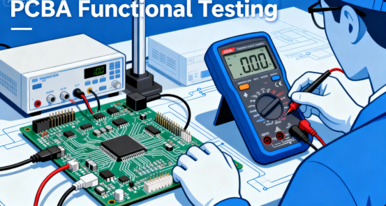
PCBA Functional Testing, short for Printed Circuit Board Assembly Functional Testing, involves placing the pcb assembly under test (UUT) in a simulated operating environment—applying appropriate stimuli and loads. This process makes the PCBA operate in various design states, allowing technicians to measure parameters for each state and verify whether its functionality meets the original design specifications.
In simple terms, it’s about applying the right signals to the pcb assembly and measuring the responses from its outputs to check if they align with design requirements. This is typically the final step and serves as the final verification stage after the board is powered on. Its core purpose is to catch poorly assembled boards. By simulating the board’s complete function as if it were installed in the final product, this test identifies potentially faulty assemblies before they are built into the finished device.
Why is PCBA Functional Testing So Important?
Why does this test hold such critical importance? As labor costs rise and quality standards become ever more stringent, functional testing has become a key process for guaranteeing product quality. Comprehensive testing services are integral to PCB manufacturing, ensuring that high quality PCBs are produced by identifying and addressing defects at every stage.
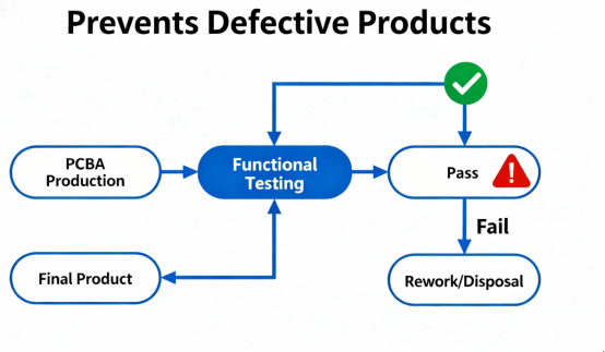
In today’s highly competitive electronics market, functional testing helps prevent defective products from reaching the market, avoiding the enormous costs and reputational damage associated with field failures and product recalls.
By identifying and eliminating problems early in the process, functional testing significantly reduces rework costs later and mitigates the risk of recalls. For industries with strict demands on product quality and reliability—such as medical, automotive, and aerospace—a comprehensive suite of functional testing methods is a non-negotiable requirement to meet regulatory and standard compliances and ensure product reliability.
What Problems Can Functional Testing Uncover?
PCBA Functional Testing can pinpoint a variety of potential issues, including:
·Power Issues: The test can reveal problems with power stability during PCB operation, such as fluctuations, dropouts, or abnormal current consumption, which may indicate defects in power regulation or delivery.
·Signal Integrity Issues: Test procedures can detect distortion, signal noise, or data corruption, especially problems with signal integrity in high-frequency environments.
·Inaccurate Voltages: Incorrect output voltages can stem from missing, defective, or incorrectly installed electronic components. Correct voltage measurement ensures the board and its electronic components function correctly.
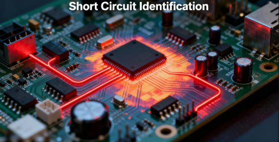
·Continuity and Isolation Problems: It checks electrical continuity and isolation, confirming that traces are correctly connected without any shorts.
·Component Interaction Faults: Functional testing can uncover design flaws that In-Circuit Test (ICT) might miss, failures caused by interaction between components, and complex functional problems. ICT focuses on testing individual components, while functional testing evaluates the performance of the entire assembly.
Functional testing helps identify defects such as missing components, ensuring all parts are properly tested before final assembly.
Common Methods for PCBA Functional Testing
Depending on product requirements, production volume, and budget, several functional testing methods and test types are available as part of the pcb assembly process. These pcb tests are integrated into the overall pcb assembly process to ensure quality and reliability. The processes involved in functional testing are designed to validate the performance of the assembly, and the tests measure key parameters such as electrical functionality, load capacity, and compliance with industry standards.
Reference System Testing
This is the simplest method—placing the Device Under Test (DUT) into a reference system or subsystem identical to its real-world environment to see if it works correctly.
While straightforward, this approach has many drawbacks, is often inefficient, and is sometimes used only to supplement other test solutions.
Test Benches
A test bench is a traditional test setup involving interfaces for stimulating the UUT and measuring its responses, controlled according to a specific test sequence.
Its advantage lies in relatively low cost and simple equipment, but it lacks flexibility when dealing with multiple products.
Special Test Equipment (STE)
This is a system that automates test bench operations. STE consists of specialized testing equipment designed to automate and streamline the testing process. Its core is typically a computer, controlled by a special bus and some programmable instruments.
Through automation, setup times, test times, and overall operation are faster and easier than manual test benches. STEs are commonly used in production or repair centers.
Automated Test Equipment (ATE)
General-purpose Automated Test Equipment is a highly advanced and flexible solution capable of meeting the testing needs of various products and programs.
Beyond the advantage of full instrument integration, ATE often provides superior solutions for signal routing and connectivity, significantly simplifying costs and making test programs easier to implement.
Based on the level of control, these tests can also be categorized as Manual, Semi-Automatic, and Fully Automatic PCBA Functional Testing.
Bed-of-Nails Test Fixtures
This method uses pre-designed test points on the circuit board. Probes bring signals out to perform a complete functional test.
During testing, the board is simply placed into the test fixture. A mechanical action pushes a set of probes (the “bed of nails”) to make contact with the test points on the board. These probes typically use pogo pins, which are spring-loaded contact points that establish reliable electrical connections with the test points on the board. This allows the UUT to be simulated as if it were connected in the final product.
Automated X-Ray Inspection in PCBA Testing
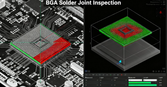
Automated X-Ray Inspection (AXI) has become an increasingly important testing method in the printed circuit board assembly (PCBA) process, especially as electronic devices grow more complex and compact. Unlike traditional visual inspection or electrical testing, AXI is a non-destructive testing method that allows manufacturers to look inside the circuit board without physically altering it. This is particularly valuable for inspecting components such as Ball Grid Array (BGA) packages, flip-chip devices, and other parts with hidden solder joints that are not accessible by standard test probes.
During automated x ray inspection, X-rays penetrate the printed circuit and generate high-resolution images of the internal structure of the circuit board. Advanced computer vision software then analyzes these images to detect defects such as solder voids, cracks, misalignments, and other anomalies that could compromise the proper functioning of the device. This process enables manufacturers to identify potential issues and defects that might otherwise go unnoticed, ensuring that every component and solder joint meets stringent quality standards.
AXI is an essential part of the PCBA testing process, providing valuable insights into the integrity of solder joints and the placement of components within the circuit. By using this testing method, manufacturers can detect defects early, reduce the risk of field failures, and maintain high product quality throughout the electronics manufacturing process.
Flying Probe Testing: An Alternative Approach
Flying Probe Testing offers a flexible and cost-effective alternative to traditional in-circuit testing (ICT) methods for circuit boards. Instead of relying on custom test fixtures, this testing method uses robotic probes—often called flying probes—to make contact with test points across the circuit board. These probes can move quickly and precisely, allowing for the measurement of electrical properties such as resistance, capacitance, and continuity at various locations on the board.
One of the key advantages of flying probe testing is its adaptability. It is particularly well-suited for low-to-medium volume production runs, where the cost and time required to create custom fixtures for each design would be prohibitive. This testing method is also ideal for circuit boards with complex layouts, high-density solder connections, or frequent design changes, as it can be easily reprogrammed to accommodate new test points and components.
Flying probe testing is highly effective at detecting defects such as open circuits, short circuits, and incorrect component values. By thoroughly checking solder connections and verifying the integrity of each component, this testing method helps ensure that the final product meets rigorous quality standards. For manufacturers seeking to improve product quality and reduce the risk of defects in their circuit boards, flying probe testing is a reliable and efficient solution within the broader suite of PCB testing practices.
Key Aspects of PCBA Functional Testing
A typical PCBA Functional Test covers the following areas:
·Power Section Test: Checks if the power supply operates correctly, measuring voltages at various points—often using comparators or other instruments.
·Port (Interface) Test: Checks for abnormalities like shorts and opens.
·Integrated Circuit Module I/O Read/Write Function Test: Includes testing for Flash, EEPROM, CPU, SDRAM, and logic ICs.
·Special Function Test: Tests specific functions required by different boards. For example, a product with infrared functionality would require an external receiver for this test.
·Robustness Testing: Subjects the PCB to temperature cycles, vibration, and shock tests to verify its resilience and durability, ensuring it can withstand different environmental conditions.
Strategies for Improving PCBA Functional Test Efficiency
With rapid technological advancement, and to save costs and boost efficiency, some PCBA functional tests have adopted fully automated solutions. Manual testing can be time consuming, which is why automation is increasingly adopted to improve efficiency. Here are key strategies for enhancing test efficiency:
Automated Test Systems
Automated test systems, like universal automated test systems for PCBA, can test a wide range of boards, becoming a general-purpose solution.
By collecting parameters from a golden sample board and setting acceptable error margins, these systems compare the UUT against the standard and determine pass/fail status. Test speed can be 5-10 times faster than manual testing.
Optimized Test Fixture Design
Well-designed test fixtures significantly improve testing efficiency and accuracy. Key design considerations include:
·Structural Stability and Reliability: The fixture's mechanical structure must be robust enough to withstand repeated pressing and unplugging during testing.
·Accuracy and Low Impedance of Electrical Connections: The connection between probes and test points must be reliable, with contact resistance kept as low as possible.
·Ease of Use and Safety: Fixture design should fully consider the operator's ergonomics and safety.
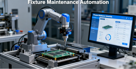
Modularity and Maintainability
Adopting a modular design facilitates fixture maintenance and upgrades. For instance, a removable probe plate allows for easy replacement and servicing, extending the fixture's lifespan and reducing long-term operational costs.
Future Trends
As electronic products trend towards miniaturization and higher intelligence, PCBA Functional Testing faces new challenges and opportunities. Future testing will place greater emphasis on:
·High-Speed Digital Signal Testing: As signal speeds continuously increase, testing for signal integrity becomes more critical.
·RF (Radio Frequency) Testing: With the proliferation of IoT and 5G technologies, more products integrate wireless functions, making RF testing a vital part of functional validation.
·Automation and Intelligence: Fully automated test systems will become more widespread, incorporating AI and machine learning for intelligent diagnostics and predictive maintenance
Conclusion
PCBA Functional Testing is an indispensable and critical step in modern electronics manufacturing. It is not just the "final gatekeeper" for product quality but also a vital means for manufacturers to reduce costs and enhance customer satisfaction. Through comprehensive functional testing, manufacturers can identify and resolve potential issues before products leave the factory, ensuring that every electronic device released to the market is reliable, safe, and conforms to its design standards.
In an era where electronics are increasingly ubiquitous, rigorous PCBA Functional Testing is the essential bridge connecting innovative design with high-quality products. It is a decisive factor for electronics manufacturers striving to win in the competitive marketplace.
FAQs
Q. What is PCBA Functional Testing?
A. Simulating real-world operating conditions to verify whether the PCBA implements its intended functions (e.g., communication, control), ensuring normal operation.
Q. What preparations are needed before testing?
A. Set up a compatible power supply/peripheral environment, define test cases clearly, and prepare tools like multimeters, oscilloscopes, or custom test fixtures.
Q. What are the common testing methods?
A. Manual verification (for simple boards), automated testing with fixtures (for complex boards), and PC software-based testing (for boards with communication interfaces).
Q. What are the most common causes of test failures?
A. Cold solder joints / poor soldering, incorrect / reversed component placement, short circuits / open circuits, firmware issues, and electrostatic discharge (ESD) damage.
Q. How to quickly locate a fault?
A. First, check for shorts between power and ground. Then, use instruments to measure signals at key test points, and analyze circuit/element issues with reference to the design schematics.
Q. What standards must the testing comply with?
A. Refer to IPC industry standards and product design specifications. Certain scenarios require compliance with international (e.g., IEC) or specific industry-specific standards.
Author: Jack Wang

