


Single-Sided Printed Circuit Boards: Benefits, Uses, and Design Tips
In the world of electronics, simplicity often drives efficiency—and that’s where single-sided printed circuit boards (PCBs) shine. These fundamental components form the backbone of countless devices, from everyday consumer gadgets to educational DIY kits. Unlike their multi-layer counterparts, single-sided PCBs feature a single conductive layer, making them cost-effective, easy to manufacture, and ideal for straightforward circuit designs.
Whether you’re a hobbyist embarking on your first electronics project or a designer looking to streamline production, understanding the benefits, applications, and design strategies of single-sided PCBs is essential.
Introduction to Single-Sided Printed Circuit Boards (PCBs)
Definition and Structure
A single-sided printed circuit board (PCB) is a type of PCB that has only one layer of conductive material, usually copper, on one side of an insulating substrate. This single copper layer is used to form the electrical connections between components mounted on the board. The other side of the board is typically used for placing components or left as a plain insulating surface.
Structurally, a single-sided PCB consists of three main parts:
1. Substrate – the non-conductive base, providing mechanical support.
2. Copper layer – etched to create the circuit pathways.
3. Components – mounted on the copper side or opposite side depending on design.
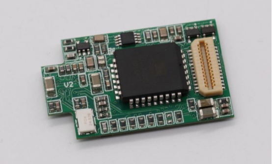
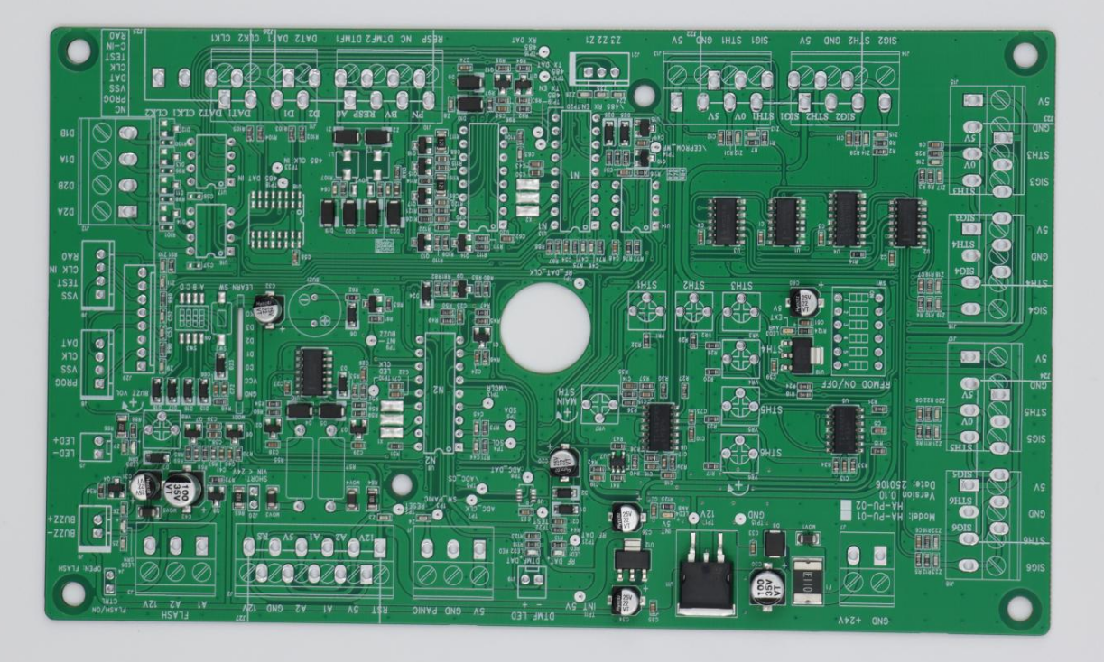
Compared to double-sided PCBs, which have copper layers on both sides of the board, single-sided PCBs are simpler and easier to manufacture but less suitable for high-density circuits. Multi-layer PCBs have multiple copper layers separated by insulating material, offering more compact designs and advanced functionality, but they are costlier and more complex to produce.
Example: A simple LED circuit on a single-sided PCB only requires one layer of copper for all the connections, whereas a more complex microcontroller board may need double-sided or multi-layer construction.
Materials and Components
The most common substrate materials for single-sided PCBs include:
FR-4: A fiberglass-reinforced epoxy laminate, widely used for its durability and flame resistance.
Phenolic paper: A lower-cost option for simple, low-performance circuits.
CEM-1/CEM-3: Composite epoxy materials used in budget electronics.
Typical components mounted on single-sided PCBs include:
Resistors and capacitors for controlling current and voltage.
Diodes and LEDs for signal or light functions.
Integrated circuits (ICs) for processing tasks in small, low-complexity devices.
Step-by-step example: In a basic toy circuit, the IC is mounted on the copper side, with resistors and LEDs connected via etched traces. This straightforward layout highlights the simplicity of single-sided PCBs.
Importance in Electronics
Despite the prevalence of advanced multi-layer boards, single-sided PCBs remain widely used due to their simplicity, reliability, and cost-effectiveness. They are especially important in:
Low-complexity circuits where only a few components are needed.
Consumer electronics, such as calculators, remote controls, and toys.
Educational kits and DIY projects, providing a hands-on learning platform for beginners.
Example: In small household gadgets like a digital clock, a single-sided PCB is sufficient to connect all components, maintain durability, and keep manufacturing costs low.
These characteristics make single-sided PCBs a practical choice for electronics designers who need simple, reliable, and cost-efficient solutions without sacrificing basic functionality.
Key Benefits of Single-Sided PCBs
Cost-Effectiveness
One of the primary advantages of single-sided PCBs is their lower production cost compared to double-sided or multi-layer boards. Because they contain only one conductive layer, the manufacturing process requires fewer materials, less labor, and simpler equipment.
Example: Small consumer electronics such as calculators, remote controls, or simple LED circuits often use single-sided PCBs. These boards provide all necessary electrical connections at a fraction of the cost of more complex PCB types.
Simplicity and Ease of Manufacturing
Single-sided PCBs are simpler to design and assemble because they contain only one conductive layer. Fewer layers reduce the complexity of routing electrical connections and make troubleshooting easier.
Step-by-Step Manufacturing Process for Single-Sided PCBs:
1. Substrate Preparation: Cut the insulating material (FR-4 or phenolic) to size.
2. Copper Lamination: Apply a copper layer on one side of the substrate.
3. Circuit Etching: Remove excess copper using a chemical etchant to form the circuit pattern.
4. Drilling: Drill holes for through-hole components if needed.
5. Solder Mask & Silkscreen: Apply protective layers and mark component positions.
6. Component Assembly: Mount resistors, capacitors, LEDs, and ICs.
This streamlined process makes single-sided PCBs ideal for beginners, small-scale production, and low-volume projects.
Reliability and Durability
Single-sided PCBs are less prone to short circuits and design errors because all connections are on a single layer. The reduced complexity improves reliability, particularly in low-power, low-density circuits.
Case Study: Educational kits and small household appliances frequently use single-sided PCBs. For example, a simple LED kit for learning electronics maintains consistent performance without layer-to-layer shorting risks.
Quick Prototyping
Another major benefit is rapid prototyping. Designers can quickly create functional prototypes without the time and cost associated with multi-layer boards. This makes single-sided PCBs especially useful for Arduino shields, DIY electronics, and experimental circuits.
Example: A hobbyist building a small sensor module can use a single-sided PCB to test the circuit in hours rather than days. Adjustments to the layout or components can be made easily due to the straightforward design.
Single-sided PCBs provide cost savings, ease of manufacturing, reliable performance, and fast prototyping, making them an ideal choice for low-complexity electronics and educational projects. Their simplicity and practicality continue to make them a widely used solution in both hobbyist and professional applications.
Common Uses and Applications
Consumer Electronics
Single-sided PCBs are widely used in consumer electronics because they are cost-effective, simple to produce, and reliable for low-complexity circuits. Typical applications include:
Calculators – connecting keys, display, and power circuitry.
Toys – powering small motors, LEDs, and sound modules.
Remote controls – enabling button inputs to communicate with devices.
LED Lighting Systems
In LED lighting systems, single-sided PCBs provide a simple platform to mount and connect multiple LEDs in series or parallel.
Step-by-Step Design Approach for LED Boards:
Determine LED layout – spacing and orientation based on desired light pattern.
Plan circuit connections – series or parallel configuration depending on voltage and current requirements.
Design copper traces – ensure sufficient width for current-carrying capacity.
Mount LEDs and resistors – solder components onto the single copper layer.
Test for continuity and brightness – verify each LED functions correctly.
Automotive and Industrial Devices (Non-Critical Applications)
Single-sided PCBs are sometimes used in automotive and industrial devices where the circuits are low-power and non-critical. Their simplicity and cost-effectiveness make them suitable for:
Dashboard indicator lights
Small motor controllers
Sensor modules in industrial equipment
Comparison: While multi-layer PCBs are used for high-speed or high-density automotive electronics, single-sided boards are preferred for applications that do not require complex routing.
Educational and DIY Projects
Single-sided PCBs are popular in educational kits and DIY electronics projects because they are easy to understand and assemble. Compared to double-sided PCBs, they allow learners to:
Visually follow the circuit layout without complex layer stacking.
Quickly assemble circuits and troubleshoot errors.
Experiment with modifications and component substitutions.
Example: Beginner Arduino shields and basic sensor modules often use single-sided PCBs to simplify learning and prototyping.
Single-sided PCBs find use across consumer electronics, LED lighting, non-critical automotive and industrial devices, and educational/DYI projects. Their simplicity, cost-effectiveness, and ease of assembly make them the go-to choice for low-complexity applications.
Design Tips for Single-Sided PCBs
Circuit Layout Planning
Effective circuit layout planning is critical for single-sided PCBs because all connections must fit on a single copper layer. Proper component placement reduces trace crossings, improves reliability, and simplifies assembly.
Best Practices for Component Placement:
Place high-power components near edges or areas with better airflow.
Group related components to minimize long traces.
Orient similar components consistently for easier soldering.
Step-by-Step Example: Minimizing Trace Crossing:
1. Identify all components and their connections.
2. Arrange components so that most connections flow in the same direction.
3. Place passive components (resistors, capacitors) close to the IC pins they support.
4. Adjust positions iteratively to reduce crossing traces, using the shortest possible paths.
Trace Routing Techniques
Efficient trace routing ensures electrical performance and prevents short circuits. Since single-sided PCBs have only one copper layer, routing must be strategic.
Guidelines for Trace Paths:
Keep traces as short and direct as possible.
Use consistent widths for current-carrying traces.
Avoid 90-degree bends to reduce signal reflections.
Using Jumpers or Wire Bridges:
When a trace cannot cross another, use a jumper wire to bridge connections.
Example: Two traces need to intersect; route one trace partially on the copper and use a small insulated wire to complete the connection.
Thermal and Electrical Considerations
Even simple PCBs must account for heat and voltage distribution. Poor thermal or electrical design can reduce board performance or cause failures.
Thermal Guidelines:
Place heat-generating components with enough spacing.
Use wider traces for components carrying higher current to dissipate heat efficiently.
Electrical Guidelines:
Keep long traces as short as possible to avoid voltage drops.
Group power and ground traces for stability.
Design Tools and Software Recommendations
Using PCB design software simplifies layout, routing, and validation. Popular tools for single-sided PCBs include:
KiCad: Free, open-source tool with schematic capture and layout capabilities.
Eagle: Offers intuitive interface and library support for small boards.
Altium Designer: Professional-grade software for complex designs, also supports single-layer boards.
Features to Optimize Single-Sided Layouts:
Automatic trace width calculation.
Design rule checks (DRC) for trace spacing and clearance.
Visual guides for component placement and alignment.
Successful single-sided PCB design combines careful layout planning, efficient trace routing, thermal and electrical awareness, and the right software tools. Following these best practices ensures functional, reliable, and easy-to-manufacture boards for both hobbyist and professional applications.
Manufacturing and Testing Guidelines
Fabrication Process
The fabrication process of single-sided PCBs is straightforward due to their single copper layer. A typical step-by-step workflow includes:
Substrate Preparation: Cut the insulating base material (FR-4, phenolic, or CEM) to the desired board size.
Copper Lamination and Etching: Apply a copper layer to one side and chemically etch unwanted copper to form the circuit pattern.
Drilling: Drill holes for through-hole components or mounting points.
Solder Mask Application: Apply a protective layer over copper traces to prevent accidental shorts.
Silkscreen Printing: Print reference labels for components, pin numbers, and orientation markers.
Example: A simple LED driver board uses this process to create a single-layer copper trace layout, ready for component assembly.
Quality Control and Testing
Quality control (QC) ensures that the manufactured PCB functions correctly and meets design specifications. Common QC methods include:
Continuity Testing: Verifies that all electrical connections are intact.
Visual Inspection: Checks for broken traces, scratches, or misaligned components.
Functional Testing: Powers the board and ensures it performs as intended.
Tips for Preventing Common Errors:
Ensure copper etching is complete to avoid unintended shorts.
Verify drill alignment before assembly.
Inspect solder mask coverage to prevent exposed copper areas.
Example: Before shipping a batch of calculator PCBs, manufacturers perform continuity and functional tests to catch defective boards.
Assembly and Soldering Best Practices
Proper assembly and soldering are critical for PCB reliability. Single-sided PCBs support both through-hole and surface-mount components, but each has unique considerations:
Through-Hole Components: Insert component leads into drilled holes and solder on the copper side.
Surface-Mount Components (SMD): Place directly on copper pads; solder using reflow or hand techniques.
Avoiding Solder Bridges:
Maintain adequate spacing between pads.
Use flux to guide solder flow.
Inspect joints visually or with a magnifier to catch accidental connections.
Example: In a small LED kit, through-hole LEDs are mounted on a single-sided board with careful soldering to avoid bridging pins.
By following these fabrication, testing, and assembly guidelines, designers and manufacturers can ensure that single-sided PCBs are functional, reliable, and easy to assemble, whether for hobby projects or commercial products.
Comparisons and Limitations
Single-Sided vs. Double-Sided PCBs
Single-sided and double-sided PCBs differ in cost, complexity, and suitable applications. The following table summarizes the key differences:
Feature | Single-Sided PCB | Double-Sided PCB |
|---|---|---|
Copper Layers | 1 layer | 2 layers |
Cost | Low | Moderate to high |
Complexity | Simple design, easy assembly | More complex routing and assembly |
Density | Suitable for low-density circuits | Supports higher-density circuits |
Applications | Calculators, toys, LED circuits, educational kits | Microcontrollers, communication boards, advanced electronics |
Troubleshooting | Easy | More challenging due to multiple layers |
Example: A small LED night light can efficiently use a single-sided PCB, while a microcontroller-based IoT sensor module often requires a double-sided PCB to accommodate additional connections and components.
Limitations
While single-sided PCBs are practical for many applications, they have inherent limitations:
Not suitable for high-density or high-speed circuits: Single-sided boards cannot accommodate dense component layouts or complex signal routing needed for modern high-speed electronics.
Design constraints in complex applications: With only one copper layer, designers may face difficulty routing all required connections, often needing jumpers or alternative design strategies.
Example: A smartphone motherboard cannot rely on a single-sided PCB because the design requires multiple layers to handle high component density and fast data signals.
Single-sided PCBs excel in cost-efficiency, simplicity, and ease of assembly, but their limited density and routing capacity make them unsuitable for high-performance or complex electronics.
Conclusion
Single-sided PCBs are valued for their cost-effectiveness, simplicity, reliability, and rapid prototyping capabilities. They are particularly well-suited for low-density, low-complexity circuits found in consumer electronics, LED lighting, educational kits, and DIY projects. The straightforward design and assembly process makes them a practical choice for both hobbyists and small-scale production.
Designers should consider using single-sided PCBs when the circuit involves limited components and low signal density, or when budget and simplicity are priorities over advanced functionality. They are also ideal for prototyping and educational applications, where ease of assembly and troubleshooting is important. To maximize performance, careful component layout planning, proper trace width selection, and effective thermal management are essential. Utilizing reliable PCB design software further ensures accuracy and reduces errors during the design process.
For those seeking professional guidance or custom PCB solutions, PCBMASTER offers expert support. Whether you need advice on optimizing single-sided layouts, selecting appropriate materials, or improving board performance, PCBMASTER can provide tailored recommendations to help bring your electronics projects to life.
FAQs
What types of electronic projects are best suited for single-sided PCBs?
Single-sided PCBs are best suited for low-density, low-complexity projects. Common examples include consumer electronics (calculators, toys, remote controls), LED lighting circuits, educational kits, and DIY hobby projects. They are ideal when the design involves limited components and simple connections that can fit on a single copper layer.
Can single-sided PCBs handle high-current applications?
Single-sided PCBs can handle moderate currents if traces are properly sized and copper thickness is sufficient. However, they are generally not recommended for high-current or high-power applications, because the single copper layer may not provide enough conductive capacity, and heat dissipation is limited compared to double-sided or multi-layer PCBs.
How do single-sided PCBs compare with double-sided PCBs in cost and reliability?
Cost: Single-sided PCBs are cheaper due to fewer materials and simpler fabrication processes. Double-sided PCBs are more expensive because they require additional copper layers, drilling, and more complex assembly.
Reliability: Single-sided PCBs are reliable for low-density, low-speed circuits, with fewer chances of layer-to-layer shorts. Double-sided PCBs are needed for high-density or complex circuits but require more careful design and manufacturing to maintain reliability.
What are common mistakes to avoid when designing single-sided PCBs?
Poor component placement, leading to long or crossing traces.
Inadequate trace widths, which can cause voltage drops or overheating.
Ignoring thermal management, especially near heat-generating components.
Failing to plan for jumpers or wire bridges when traces cannot cross.
Overcomplicating designs that would be better suited for double-sided or multi-layer PCBs.
Are there modern alternatives to single-sided PCBs for hobbyist projects?
Yes, modern alternatives include:
Double-sided PCBs: Allow higher component density and more complex layouts.
Flexible PCBs (FPCs): Thin and bendable boards suitable for compact or wearable electronics.
Multi-layer PCBs: Used in advanced hobbyist projects involving microcontrollers, IoT devices, or high-speed circuits.
Breadboards and prototyping shields: For temporary layouts and rapid prototyping without soldering.

