Circuit Board PCB Assembly Process Explained: From Design to Production
From smartphones to industrial control systems, every modern electronic device relies on printed circuit boards (PCBs) to connect and power its components. However, creating a fully functional PCB involves much more than circuit design alone. The PCB assembly (PCBA) process bridges the gap between concept and reality, transforming a bare board into a fully operational electronic product.
Understanding how this process works—from design preparation to final production—reveals the precision and expertise behind reliable electronic manufacturing.
Introduction to PCB Assembly
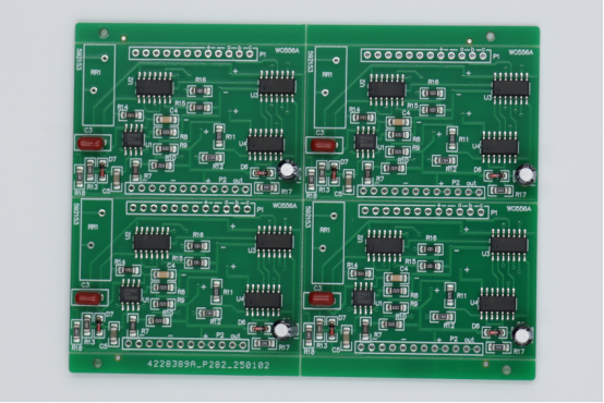
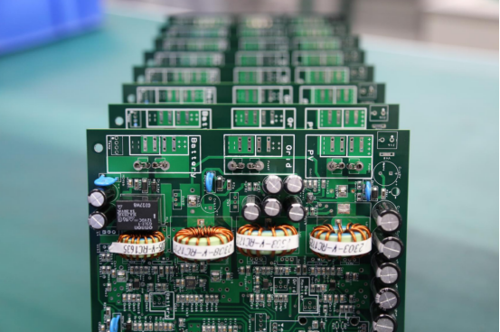
Printed Circuit Board Assembly (PCBA) is the process of mounting and soldering electronic components onto a manufactured printed circuit board (PCB) to create a complete, functional electronic device. It is one of the most critical stages in electronics manufacturing, turning a design concept into a working system that powers everything from consumer gadgets to industrial machinery.
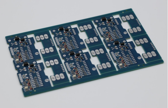
A PCB is the physical platform that provides mechanical support and electrical connections between components. PCB fabrication refers to making this bare board — a flat structure made of copper layers and insulating materials. It involves etching circuit patterns, drilling vias, and applying surface finishes. In contrast, PCB assembly begins once the bare board is ready. This stage includes applying solder paste, placing components such as resistors, capacitors, and ICs, and then soldering them through methods like reflow or wave soldering.
Think of fabrication as building the foundation, while assembly is constructing the house — installing everything that makes it functional. Without fabrication, there’s no base to build on; without assembly, the circuit can’t operate.
The end-to-end PCB production process typically begins with circuit design and schematic creation, followed by fabrication, assembly, and final testing. During testing, engineers check electrical performance, functionality, and quality before the product is approved for use.
Several key players collaborate throughout this process:
Design engineers create the schematics and layout.
Fabricators manufacture the bare boards.
Assemblers place and solder the components.
Quality control teams inspect and test the finished assemblies to ensure reliability.
Together, these roles form a continuous workflow that transforms an electronic idea into a durable, high-performance product ready for real-world application.
Understanding PCB Design – The Foundation of Assembly
Before a single component is placed on a circuit board, the process begins with PCB design — the blueprint that determines how the board will function, fit, and perform. A well-designed PCB not only defines the electrical connections but also ensures that the layout can be efficiently manufactured and assembled without costly revisions.
PCB Layout and Schematic Design
A circuit schematic is a visual map that defines how each electronic component connects within a circuit. It shows symbols for resistors, capacitors, microcontrollers, and other devices, along with the electrical pathways linking them. The schematic acts as the logical design, describing what the circuit should do.
Once the schematic is complete, engineers use Electronic Design Automation (EDA) software—such as Altium Designer, KiCad, or Cadence Allegro—to translate that logic into a PCB layout. The layout represents the physical implementation of the schematic, including copper traces, vias, component footprints, and mechanical outlines.
For example, when designing a microcontroller-based PCB, the schematic might define the microcontroller, power supply, oscillator, and interface connectors. The engineer then converts this design into a multilayer layout, carefully arranging power planes, signal traces, and ground references to minimize noise and ensure signal integrity.
A clear distinction exists between the two:
Schematic design defines electrical function.
PCB layout defines physical structure and manufacturability.
This two-step process ensures that the final board performs exactly as intended while remaining feasible for production.
Design for Manufacturability (DFM) Considerations
Design for Manufacturability (DFM) refers to optimizing a PCB design so that it can be produced accurately, efficiently, and at a reasonable cost. DFM ensures that the layout not only meets electrical requirements but also aligns with real-world assembly capabilities.
Several design elements directly affect manufacturability:
Component spacing: Adequate clearance between parts allows pick-and-place machines and soldering tools to operate without interference.
Pad size and shape: Proper pad dimensions help create reliable solder joints.
Component orientation: Consistent orientation across the board simplifies automated assembly and inspection.
Ignoring DFM guidelines can lead to common problems such as:
Insufficient solder mask clearance, causing solder bridges or shorts.
Misaligned vias, which may break signal continuity.
Non-standard component footprints, requiring manual rework or design changes.
To avoid these issues, designers should:
Follow IPC design standards (such as IPC-2221 and IPC-7351).
Review designs with assembly partners early in the process to catch potential issues.
Use DFM analysis tools within their EDA software to validate spacing, clearances, and tolerances.
By incorporating DFM principles during the design phase, engineers create boards that are not only electrically sound but also ready for seamless PCB assembly and high production yield.
Preparing for PCB Assembly
Proper preparation is essential to ensure a smooth and efficient PCB assembly process. This stage involves organizing all necessary components, files, and tools so that the assembly line can operate without delays or errors. Key steps include creating a Bill of Materials (BOM), preparing assembly files, and readying solder paste stencils.
Bill of Materials (BOM) and Component Sourcing
A Bill of Materials (BOM) is a detailed list of all components required for a PCB, including resistors, capacitors, integrated circuits, connectors, and other parts. The BOM specifies part numbers, quantities, manufacturers, and technical specifications. It acts as a central reference for both procurement and assembly teams, ensuring that no part is overlooked during production.
Component availability, lifecycle, and cost directly affect PCB assembly:
Components that are out of stock or obsolete can cause delays or force redesigns.
High-cost parts may require careful sourcing or alternative suppliers to optimize budget.
Understanding component lifecycles ensures long-term maintainability of the product.
When sourcing components, manufacturers may choose between:
In-house sourcing: The company purchases all components individually and supplies them to the assembly line. Pros include control over quality and inventory. Cons include increased management effort and logistical complexity.
Turnkey assembly services: The assembler handles both component sourcing and assembly. This reduces management overhead and often speeds production but may limit flexibility in choosing suppliers or part brands.
Gerber Files and Pick-and-Place Data
Gerber files are the industry-standard digital files that describe the physical layers of a PCB, including copper traces, solder mask, and silkscreen. Centroid (or pick-and-place) files provide precise X-Y coordinates, rotation angles, and component reference designators for automated placement machines.
Step-by-step use in assembly:
1. Stencil cutting: Gerber files guide the creation of solder paste stencils, ensuring paste is applied precisely to component pads.
2. Component placement: Pick-and-place machines read centroid files to locate and position each component on the board accurately.
3. Verification: Automated optical inspection (AOI) systems compare actual placement to these files to detect errors before soldering.
These files act as digital blueprints, allowing PCB assembly to be automated, repeatable, and accurate.
Solder Paste Stencil Preparation
A solder paste stencil is a thin sheet with openings that match the pads on a PCB, used to deposit solder paste accurately before component placement. Proper stencil preparation is critical for reliable solder joints and overall assembly quality.
Stencil materials include:
Stainless steel: Durable, widely used for high-volume production.
Nickel: Resistant to wear and chemical corrosion.
Laser-cut stencils: Provide precise openings for fine-pitch components.
Example: The thickness of a stencil directly affects solder volume. A thicker stencil deposits more paste, which may cause solder bridging on fine-pitch ICs, while a thinner stencil may lead to insufficient solder, resulting in weak joints. Selecting the right stencil thickness ensures both mechanical stability and electrical reliability.
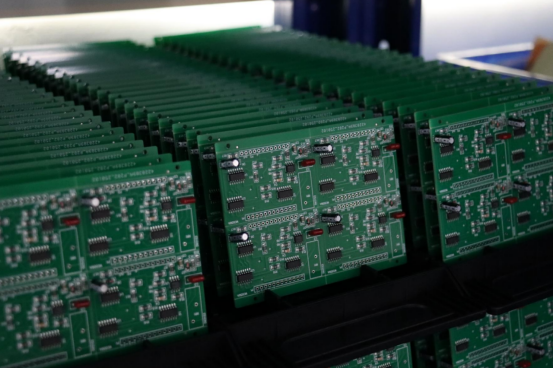
Step-by-Step PCB Assembly Process
The PCB assembly process transforms a bare board into a fully functional electronic device. It involves multiple stages, each critical for ensuring reliability, electrical performance, and manufacturability. Below is a detailed, step-by-step overview.
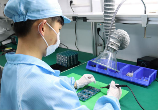
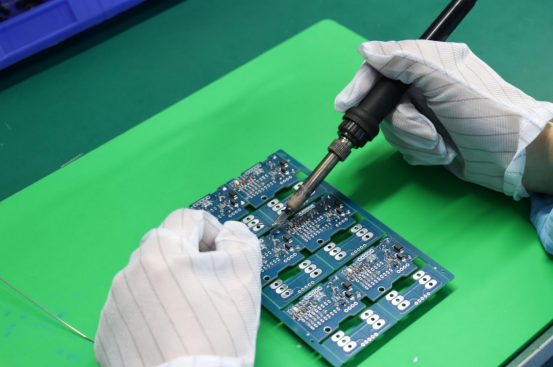
Step 1 – Solder Paste Application
Solder paste application is the first stage in mounting surface-mount components. It involves screen-printing solder paste onto the pads of the PCB, creating a temporary adhesive layer that holds components in place during assembly.
Factors influencing solder paste quality include:
Viscosity: Proper thickness ensures paste flows correctly during reflow.
Temperature: Paste must be stored and applied at controlled temperatures to prevent drying or clumping.
Alignment: Accurate stencil alignment is essential to match pads precisely.
A well-applied solder paste layer is crucial for reliable solder joints and reduces defects such as bridging or insufficient solder.
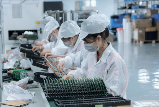
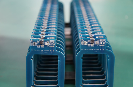
Step 2 – Pick and Place of Components
The pick-and-place step uses automated machines to place components accurately on the solder-pasted PCB.
Key machine features include:
Feeders: Supply components from reels or trays to the machine.
Vision alignment systems: Verify orientation and position before placement.
Vacuum nozzles: Pick up and place components without damage.
Example:
Surface-Mount Technology (SMT) components like resistors and ICs are placed directly onto pads.
Through-hole components such as connectors may require later manual or wave soldering.
Automation increases speed, precision, and repeatability while reducing human error.
Step 3 – Reflow Soldering
After components are placed, the PCB passes through a reflow oven, which melts solder paste to form permanent joints.
Reflow oven temperature profile:
Preheat: Gradually warms the board to avoid thermal shock.
Soak: Activates flux and stabilizes temperature across components.
Reflow: Solder melts and creates electrical connections.
Cooling: Solidifies solder joints without stress.
Common solder alloys:
SAC305: Lead-free, widely used in consumer electronics.
Sn63Pb37: Traditional leaded alloy, known for reliability in certain applications.
Common issues: tombstoning (components lifting), bridging (solder connecting adjacent pads), or cold joints (incomplete solder flow).
Step 4 – Inspection and Quality Control
Inspection ensures the PCB meets quality and functional standards before further processing.
Techniques include:
Automated Optical Inspection (AOI): Detects visible defects like misalignment, missing components, or solder bridges.
X-ray inspection: Checks hidden solder joints, such as under BGAs or fine-pitch ICs.
Rework options:
Manual rework: Technician fixes small defects by hand.
Automated rework: Machines correct errors for high-volume boards.
Key metrics evaluated: solder joint quality, component alignment, correct polarity, and overall board integrity.
Step 5 – Through-Hole Assembly and Wave Soldering
Through-hole technology is used when components require stronger mechanical connections or higher current capacity, such as connectors, transformers, or high-power resistors.
Soldering methods include:
Wave soldering: Entire PCB passes over a wave of molten solder, joining all through-hole leads simultaneously.
Selective soldering: Solder is applied only to specific pads, useful for mixed SMT and through-hole boards.
This stage ensures mechanical durability and electrical reliability for components that endure stress or heavy current.
Post-Assembly Processes
After components are mounted and soldered, the PCB moves into post-assembly processes, which ensure functionality, reliability, and protection during operation. These steps include functional testing, cleaning, coating, and final inspection before shipping.
Functional Testing and Programming
Functional testing verifies that the assembled PCB performs as intended under real operating conditions. One common method is In-Circuit Testing (ICT), which checks for proper electrical connections, component values, shorts, and open circuits.
Examples of functional tests include:
Power-on test: Confirms that the board powers up correctly and voltage levels are stable.
Communication validation: Ensures interfaces like UART, SPI, or Ethernet function properly.
Firmware flashing: Uploading embedded software to microcontrollers or programmable ICs for full operation.
Functional testing is critical for yield optimization and reliability. Detecting defects early prevents costly field failures and ensures consistent product quality.
Cleaning and Conformal Coating
Cleaning removes flux residues, dust, and ionic contamination left after soldering, which can cause corrosion or short circuits over time. Methods include aqueous cleaning, solvent-based cleaning, or ultrasonic cleaning depending on board sensitivity and component type.
Conformal coatings provide an additional layer of protection against moisture, chemicals, and mechanical stress. Common types include:
Acrylic: Easy to apply and remove, ideal for moderate protection.
Silicone: Flexible and heat-resistant, suitable for boards exposed to vibration or high temperature.
Urethane: Offers robust chemical and moisture resistance for demanding industrial applications.
Cleaning and coating increase the longevity and reliability of the assembled PCB in real-world conditions.
Final Inspection and Packaging
Before shipping, every PCB undergoes visual and electrical inspection to confirm correct assembly, solder quality, and component placement. Defects detected at this stage are reworked or rejected to maintain quality standards.
Packaging considerations:
ESD-safe materials protect sensitive components from electrostatic discharge.
Protective trays or bubble packaging prevent mechanical damage during transport.
Clear labeling ensures traceability and compliance with shipping and customer requirements.
Final inspection and proper packaging guarantee that the PCB arrives safe, functional, and ready for integration into the end product.
Quality Standards and Certifications
Maintaining high-quality standards and adhering to recognized certifications is critical in PCB assembly. These standards ensure reliability, safety, and consistency in electronic products, giving manufacturers and customers confidence in the final product.
IPC Standards for PCB Assembly
IPC standards are globally recognized guidelines for electronic assembly quality. Two key standards include:
IPC-A-610: Defines acceptability criteria for electronic assemblies, including solder joint quality, component placement, and board cleanliness. It is widely used for production inspection and auditing.
IPC-J-STD-001: Focuses on requirements for soldering materials, processes, and workmanship, ensuring solder joints are reliable and meet industry expectations.
Class distinctions in IPC standards:
Class 1: General electronics for consumer products where function is important, but occasional failure is acceptable.
Class 2: Dedicated service electronics, where continued performance and extended life are required.
Class 3: High-reliability applications, such as aerospace, or medical electronics, where failure is critical.
Using IPC standards ensures that assembly processes, soldering quality, and inspection criteria meet industry best practices and can be consistently reproduced across batches.
ISO and RoHS Compliance
ISO 9001 is a quality management system standard that defines structured processes for consistent production, documentation, and continuous improvement. Compliance ensures that a manufacturer can deliver reliable PCBs consistently.
RoHS (Restriction of Hazardous Substances) regulates the use of hazardous materials, such as lead, mercury, or cadmium, in electronic products. RoHS compliance ensures that PCBs meet environmental and safety regulations, protecting users and the environment.
Benefits of compliance:
Builds customer trust by demonstrating commitment to quality and environmental responsibility.
Facilitates access to global markets where regulatory compliance is mandatory.
Reduces risk of product recalls, legal issues, and reputational damage.
Together, IPC, ISO, and RoHS standards form a framework for reliable, safe, and high-quality PCB assembly, ensuring that both consumer and high-reliability products meet rigorous expectations.

Common Challenges and Best Practices
Even with advanced automation and careful design, PCB assembly can face challenges that affect quality, reliability, and production efficiency. Understanding common defects and implementing best practices is essential for successful manufacturing.
Common Assembly Defects
PCB assembly defects occur when components or solder joints fail to meet specifications. Common defects include:
Bridging: Occurs when solder unintentionally connects two adjacent pads or leads. Causes include excessive solder paste or poor stencil alignment. Prevention involves precise stencil design, correct solder paste volume, and inspection.
Tombstoning: A small component, such as a resistor, lifts on one end during reflow soldering. Causes include uneven heating or imbalanced pad sizes. Proper temperature profiling and balanced pad design can reduce this defect.
Solder balling: Small spheres of solder appear outside intended pads. Often caused by flux residues or excessive solder paste. Cleaning flux residues and optimizing paste deposition can prevent solder balls.
Example-based analysis:
On a microcontroller board, bridging between fine-pitch pins can short multiple circuits, causing functional failure. Tombstoning on a small resistor may lead to intermittent connections. By analyzing defects in previous batches, assembly engineers can adjust processes and prevent recurrence.
Best Practices for Reliable PCB Assembly
Implementing best practices helps ensure high-quality and repeatable assembly results:
Design collaboration with assemblers: Early coordination between designers and assembly teams identifies potential manufacturability issues and reduces rework.
Regular inspection cycles: Use automated and manual inspections at critical stages. Combine data logging and traceability systems to track defects and production trends.
Continuous improvement via feedback loops: Collect data from production, testing, and customer returns. Use insights to refine processes, update design guidelines, and optimize soldering profiles.
By following these practices, manufacturers can minimize defects, improve yield, and maintain high reliability for both consumer and high-performance PCBs.
Trends and Innovations in PCB Assembly
The PCB assembly industry continues to evolve, driven by the need for smaller, faster, and more sustainable electronics. Emerging technologies and process innovations are reshaping how manufacturers design, assemble, and test printed circuit boards.
Miniaturization and Advanced Packaging
Modern electronics demand smaller and more densely packed components. Technologies such as micro-BGAs (Ball Grid Arrays), CSPs (Chip-Scale Packages), and fine-pitch ICs enable compact designs but also introduce assembly challenges.
Challenges include:
Limited space for soldering and placement.
Increased risk of bridging, tombstoning, or misalignment.
Difficulties in inspection due to hidden solder joints.
Solutions:
High-precision pick-and-place machines with sub-micron accuracy.
Advanced solder paste printing and optimized stencil design.
Use of X-ray inspection and 3D AOI to verify hidden joints.
These innovations allow manufacturers to produce high-density, high-performance PCBs for mobile devices, wearables, and industrial electronics.
Automation and Smart Factories
Automation is transforming PCB assembly into smart, data-driven processes.
Applications of AI and machine learning include:
Optimizing pick-and-place operations to reduce cycle time and placement errors.
Real-time defect detection using vision systems and predictive analytics.
Predictive maintenance of assembly equipment to prevent downtime.
Smart factories integrate IoT sensors, cloud analytics, and machine learning algorithms to continuously monitor production, improve yield, and reduce operational costs. This results in faster production, higher quality, and more consistent assemblies.
Sustainable PCB Assembly
Environmental responsibility is becoming a major focus in PCB manufacturing. Sustainable practices include:
Lead-free soldering processes, reducing toxic materials.
Material recycling and waste reduction, such as reusing solder paste or reclaiming copper from scrap boards.
Energy-efficient equipment, minimizing electricity consumption during reflow and wave soldering.
Comparison:
Traditional assembly lines often rely on leaded solder, solvent-based cleaning, and energy-intensive ovens.
Eco-friendly assembly lines adopt RoHS-compliant solder, water-based cleaning, and optimized thermal profiles to reduce energy use and environmental impact.
Sustainable PCB assembly not only meets regulatory standards but also appeals to environmentally conscious customers and improves the long-term viability of production.
Conclusion
PCB assembly serves as the critical bridge between electronic design and fully functional devices. Without precise soldering, accurate component placement, and thorough testing, even the best-designed circuit cannot perform reliably.
Success in PCB assembly relies on precision, rigorous quality control, and close collaboration between design engineers, fabricators, and assembly teams. Attention to detail at every stage—from layout and component sourcing to inspection and testing—ensures high yield, long-term reliability, and consistent performance.
For businesses and engineers seeking dependable PCB solutions, partnering with experienced assembly providers like PCBMASTER can streamline production, reduce risks, and deliver high-quality, ready-to-use circuit boards that meet both technical and environmental standards.
FAQs
What is the difference between PCB fabrication and PCB assembly?
PCB fabrication is about making the bare circuit board—etching copper traces, drilling holes, and applying solder masks. PCB assembly, on the other hand, is mounting and soldering electronic components onto the board to make it functional. Simply put, fabrication gives you the board, assembly brings it to life.
How long does the PCB assembly process take from design to completion?
The timeline depends on board complexity, components, and production scale. A simple board may take 1–4 weeks, while complex multilayer or high-density boards can take 6–12 weeks or more. The process includes design, BOM preparation, fabrication, component placement, soldering, inspection, and testing.
What factors affect the cost of PCB assembly?
Key factors include:
Components: Rare or expensive parts increase cost.
Board complexity: More layers, fine-pitch ICs, or dense layouts raise difficulty.
Quantity: Larger production runs usually lower the per-unit cost.
Testing and quality: Functional testing, AOI, or X-ray inspection adds expense.
Assembly type: SMT, through-hole, or mixed-technology assembly affects labor and equipment.
What is the role of solder paste in PCB assembly?
Solder paste acts as a temporary adhesive and conductor for surface-mount components. During reflow soldering, it melts to form permanent electrical and mechanical connections. Proper paste application ensures reliable solder joints, prevents shorts, and supports precise automated placement.
How can I ensure high quality in my PCB assembly projects?
To achieve high-quality assembly:
Design for manufacturability (DFM): Use correct pad sizes, spacing, and orientations.
Work with experienced assembly partners: Early collaboration can prevent errors.
Inspect and test thoroughly: Use AOI, X-ray, ICT, and functional testing.
Track processes: Maintain traceability and monitor defect trends.
Follow industry standards: IPC-A-610, IPC-J-STD-001, ISO 9001, and RoHS compliance ensure reliability and safety.