Understanding Rigid-Flex PCB Stack-Up Designs and Materials
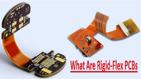
Rigid-flex PCBs are made from a combination of rigid and flexible boards, and are commonly used in the electronics industry. A rigid-flex PCB stack-up involves a complex structure that requires careful attention to both the layer arrangement and the material choices.
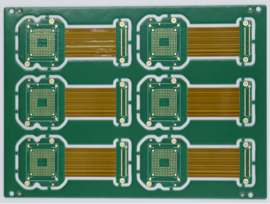
In a rigid-flex PCB stack-up, rigid and flexible parts of the board are integrated into a single assembly. The rigid layers are typically made from FR4 material, while the flexible parts are made from polyimide, known for its high flexibility. The stack-up design places rigid layers on the outside and flexible layers in between, creating a sandwich-like structure. This combination of materials and layer design allows the flexible parts to provide bending and folding capabilities, while the rigid parts offer stability for component connections. Together, the right materials and stack-up structure enable the creation of 3D designs that are ideal for space-constrained applications.
Detailed Analysis of Stack-up Configurations
Simple Stack-up Design (1R+2F+1R)
This is a basic type of rigid-flex stackup that is commonly used. Its layer configuration is that first rigid material layer, then 2 flexible material layers, and in the fourth position, a rigid layer.
Its central flexible layers are made with polyimide material, and their sides have copper layers for interconnection with rigid parts, which maintain electrical continuity through easy bending and folding.
Its main advantage is that fewer layers help to make these boards easily, using low cost, and it also has minimal bonding layers.
The rigid part provides structural support, and the flex layers manage mechanical movement.
Its disadvantage is that the two-layer flex design bears normal bending forces, but if dynamic flexing is involved, it can break the structure.
It is not best to support high-density interconnects or complicated paths of signals since it uses two flexible copper layers. It is also not preferred for controlled impedance applications.
1R + 2F + 1R stack-up is commonly part of compact interconnections and not preferred for high signal routing.
It is normally employed in earbud circuits and smartwatch circuit assemblies. cameras and some medical devices, like health monitoring tools
Complex Stack-Up Designs
In this design of stack-up, extra flexible layers or rigid layers are used for enhanced flexibility and high-density routing.
(1R + 2F + 1R + 1) Stack-Up
In this stackup design, more rigid layers are used for high support, and this structure provides a larger number of signal layers in rigid materials.
The main advantage of this design is that a larger number of layers helps to get a routing channel with compatibility for HDI routing for multilayers. It strongly connects electronic components like resistors, transistors, and connectors.
Its main disadvantage is production of these designs is complicated since it needs more lamination cycles. Layer density also produces more heat. Complex design causes a difficult impedance configuration in HF signals.
These stacks are used in medical diagnostic devices and HF communications systems.
(1 + 1R + 2F + 1R + 1) Stack-Up
In this design, 2 rigid layers are employed on the sides of the flexible layers. These configurations are part of circuits where controlled impedance with dense interconnections is needed.
The main advantages are that on this assembly we can make buried microvias and blind vias.
It maintains signal quality, since power planes and ground planes control noise.
Its disadvantage is that HDI involvement increases the overall cost of the stackup. It is a production and repairing difficult processtake time. also causes a mismatch of thermal expansion between flexible and rigid layers.
It is used in RF antennas and circuits where high frequencies are involved with that limited spacing, such as foldable devices.
(1 + 1 + 1R + 2F + 1R + 1 + 1) Stack-Up
It normally comes with layered structures that are
Layer | Type | Region | Details |
|---|---|---|---|
Layer 1 | Conductive (Cu) | Rigid | signal layer in the rigid part |
Layer 2 | Conductive (Cu) | Rigid | Inner routing/plane layer in rigid |
Layer 3 | Conductive (Cu) | Flex | Flex copper layer 1, exists in the flex part |
| Layer 4 | Conductive (Cu) | Flex | Flex copper layer 1, exists in the flex part |
| Layer 5 | Conductive (Cu) | Flex | 2nd Flex copper layer is part of flex area |
| Layer 6 | Conductive (Cu) | Rigid | End of rigid stack after flex core; return/plane layer |
| Layer 7 | Conductive (Cu) | Rigid | Internal routing layer in the rigid part |
| Layer 8 | Conductive (Cu) | Rigid | lower signal layer in rigid layer |
This stackup configuration provides impedance-controlled lines and a high-density microvia design. It is compatible with high-frequency projects, fifth generations, and radar technology.
Its disadvantage is that its complex design makes it high-cost, and laminations require accurate thermal control.
It also uses X-ray and AOI inspection methods for quality testing, which increases cost.
Special Stack-up Designs for Specific Applications
Specialized design stacks up parts of industries where harsh conditions exist, made with the use of special types of materials.
Roger material used is the best option for radio frequency circuits since it has a low dielectric constant. Polyimide has been used because it has good flexibility and manages heat. An aluminum or copper substrate is used since it provides good heat dissipation and is part of the aviation industry
These rigid-flex designs are part of the aviation industry, where mechanical strength is required. Their high reliability makes them the best option for different medical field surgical tools.
4-Layer, 6-Layer, and 8-Layer Rigid-Flex PCB Stack-ups
4-Layer
Layer No. | Material Type | Details |
|---|---|---|
1 | Top solder mask | Rigid |
2 | Top copper layer | Rigid |
3 | Prepreg | - |
| 4 | Inner copper layer | Flex |
| 5 | Flexible core | Flex |
| 6 | Inner copper layer | Flex |
| 7 | Prepreg | - |
| 8 | Bottom copper layer | Rigid |
| 9 | Bottom solder mask | Rigid |
6-Layer
Layer No. | Material Type | Details |
|---|---|---|
1 | Top solder mask | Rigid |
2 | Top copper layer | Rigid |
3 | Prepreg | - |
| 4 | Inner copper layer | Flex |
| 5 | Flexible core | Flex |
| 6 | Inner copper layer | Flex |
| 7 | Flexible core | Flex |
| 8 | Inner copper layer | Flex |
| 9 | Flexible core | Flex |
| 10 | Inner copper layer | Flex |
| 11 | Air gap | - |
| 12 | Prepreg | - |
| 13 | Bottom copper layer | Rigid |
| 14 | Bottom solder mask | Rigid |
8-Layer
Layer No. | Material Type | Details |
|---|---|---|
1 | Top solder mask | Rigid |
2 | Top copper layer | Rigid |
3 | Prepreg | - |
| 4 | Inner copper layer | Rigid |
| 5 | Core | Rigid |
| 6 | Inner copper layer | Rigid |
| 7 | Prepreg | - |
| 8 | Inner copper layer | Flex |
| 9 | Flexible core | Flex |
| 10 | Inner copper layer | Flex |
| 11 | Flexible core | Flex |
| 12 | Inner copper layer | Flex |
| 13 | Flexible core | Flex |
| 14 | Inner copper layer | Flex |
| 15 | Air gap | - |
| 16 | Prepreg | - |
| 17 | Inner copper layer | Rigid |
| 18 | Bottom copper layer | Rigid |
| 19 | Bottom solder mask | Rigid |
Key Design Considerations of Rigid-Flex PCB Stack-Up
Signal Integrity
A rigid-flex stack-up has a high effect on signal quality since it has different material structures, varied cross sections, and a flex part that has different impedance.
Reflections occur due to different dielectric constant values of polyimide and FR4 rigid and impedance discontinuities due to the adhesive.
To get the required signal quality, we should add constant reference planes over flex and rigid areas and not use splitting planes. We can also maintain quality through using low dielectric constant, low-loss adhesive in high-speed signals.
Thermal Management
In rigid-flex design, different materials are used; each has a certain value of thermal conductivity, like polyimide, which has lower thermal conductivity compared to rigid FR4, which causes a difference for thermal management.
In these conditions, flexible parts do not have accurate heat spreading since they have thin dielectric and do not have high-weight copper planes.
For solving this error or proper heat management, copper planes are used in the flex part that provides thermal conduction like the rigid part. We can also use polyimide that handles temperatures more than 200°C.
For spreading heat to the inner copper layers, thermal vias are employed in the rigid part.
Bending and Mechanical Strength
There is a need to ensure compatibility for electrical features with the mechanical strength of the rigid flex board. If we make a thick design that provides good power distribution and EMI, but affects bendability.
A larger number of flex layers provides a thick flex part but affects the bending features. Similarly, adhesive increases thickness but affects mechanical strength.
To solve this problem, make the flex part thin, about one to two layers. Follow the defined bend radius details. Do not use pads as vias in bending locations
Material Selection in Rigid-Flex PCBs
Material Overview
1. DUPONT - Polyimide (PI) Material
DuPont is a globally recognized supplier of high-performance materials. Their Polyimide (PI) material is widely used in high-end electronic products due to its excellent high-temperature resistance, electrical properties, and mechanical strength. This material is particularly suitable for applications requiring high temperatures, high frequencies, and high reliability.
Features: High-temperature resistance (over 250°C), excellent electrical properties, superior mechanical strength, low dielectric constant.
Applications: High-frequency communication, aerospace, medical devices, smartphones, and other high-end consumer electronics.
2. Panasonic - Polyimide (PI) Material
Panasonic offers Polyimide (PI) materials that provide high thermal stability and excellent electrical performance, making them ideal for high-temperature, flexible, and high-frequency applications. Panasonic materials are commonly used in communication devices and automotive electronics, where durability is crucial.
Features: High-temperature resistance, good mechanical strength, suitable for high-frequency signal transmission, excellent flexibility.
Applications: 5G communication devices, radar systems, automotive electronics, medical equipment, etc.
3. TAIFLEX - Polyimide (PI) and Polyester (PET) Materials
TAIFLEX provides a combination of Polyimide (PI) and Polyester (PET) materials, which are suitable for mid- to low-frequency applications. The PI material is used for high-temperature and high-frequency requirements, while PET material offers a cost-effective solution, making it ideal for budget-conscious products.
Features: PI material offers high-temperature resistance and mechanical strength, while PET material is more cost-effective and suited for lower-frequency applications.
Applications: Consumer electronics, home appliances, standard communication devices, low-frequency applications, etc.
4. TOSHIBA - Polyimide (PI) and Polyester (PET) Materials
TOSHIBA offers Polyimide (PI) and Polyester (PET) materials that strike a balance between cost and performance. PI materials provide good thermal stability, while PET materials are suitable for cost-sensitive markets, making them ideal for lower-frequency applications.
Features: PI material offers high-temperature resistance and mechanical strength, while PET material is suited for low-frequency, cost-effective applications.
Applications: Consumer electronics, home appliances, low-frequency circuits, etc.
PCBMASTER Real-World Example: Using Panasonic (PI) Material in Rigid-Flex PCB Design
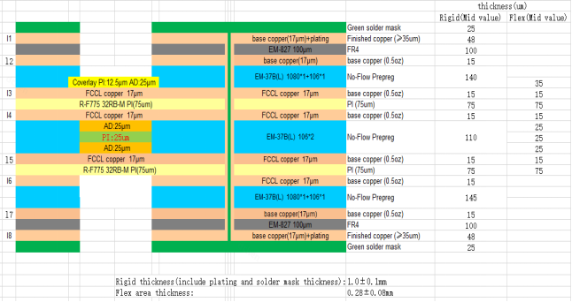
To help understand the material selection process better, let's dive into a detailed analysis of an 8-layer Rigid-Flex PCB design using Panasonic Polyimide (PI) material. We will explore how the choice of material and stack-up structure impact the final product.
Product Specifications
Flexible Area Material: Panasonic Polyimide (PI)
Thickness:
- Rigid Area: 1.0mm
- Flexible Area: 0.20mm
Layer Count: 8-layer structure (2+4+2)
Rigid Area: 2 layers (top and bottom for structural support)
Flexible Area: 4 layers (for bending and connections)
Copper Thickness:
- Inner Layers: 0.5oz
- Outer Layers: 1.0oz
Line Width/Spacing: 2.5/2.5mil
Surface Finish: 2U" Gold Immersion
Solder Mask: Green solder mask with white characters
Copper Foil Type: Rolled copper
Product Features
1. High Temperature Resistance
Panasonic PI material offers excellent heat resistance, capable of withstanding temperatures above 250°C. This makes it ideal for devices operating in high-temperature environments like automotive electronics and 5G communication equipment, ensuring the PCB remains stable over long-term use in hot conditions.
2. Flexibility and Bending Performance
The design uses a 2+4+2 layer stack-up, with the flexible region at only 0.20mm thickness, allowing the PCB to bend or fold without damage. This makes it well-suited for applications that require flexibility, such as wearable devices and medical implants.
3. Excellent Signal Transmission
With low dielectric constant and low loss characteristics, Panasonic PI material ensures stable high-frequency signal transmission with minimal signal degradation. It’s perfect for high-frequency applications like 5G communication and satellite communication.
4. Thermal Management
The use of 1.0oz copper for the outer layers and 0.5oz copper for the inner layers ensures efficient heat dissipation, preventing overheating during high-power operations. This is crucial for applications in automotive electronics and industrial control systems, where effective thermal management is required.
5. Structural Strength and Reliability
The 1.0mm thick rigid regions provide structural support, while the flexible layers maintain stability even under bending or vibration. This makes the PCB highly reliable for demanding applications like medical devices and wearable electronics.
6. High-Quality Surface Treatment
The immersion gold process enhances the PCB's contact performance and corrosion resistance, making it suitable for high-reliability high-frequency electronic devices.
This 8-layer Rigid-Flex PCB made with Panasonic PI material excels in high temperature resistance, flexibility, signal integrity, and thermal management. It is ideally suited for applications in 5G communication, automotive electronics, medical devices, and wearable technology, providing reliable performance in high-frequency, high-temperature, and space-constrained environments.
Conclusion and Practical Advice
There needs to be an expert for understanding complex features of rigid-flex PCB stackup design that helps to make reliable and high-performance projects according to demand. The proper expertise is important for making stable connections of rigid boards and stable structures with flexible circuits that make the required and innovative design of products and functions.
For getting final defined rigid-flex boards, accurate layer stackup material, and strong mechanical strength are needed. For getting optimal board performance, one must get an idea about the material properties used in the board. The use of advanced design software tools helps to make complex designs of rigid flex in simplified simulation. Altium Designer is the best option for board design, and some others are also used.
Engineers and PCB learners must also make close collaborations with PCB manufacturers like PCBMASTER for quality manufacturing. Keep updated on new methods, materials, designing processes, and production methods that make your rigid-flex PCB design innovative.
Further, to avoid redesigning or costly repairs during the board manufacturing process, one must perform detailed work during the planning of the board stack-up.
Simulation tools help to define electrical and mechanical features of the board before starting the manufacturing process.
Make a proper layout of the product from assembly to final delivery during design.
By following this practical advice, you can make high-quality, reliable, and innovative projects.
FAQs
1. What are the main advantages of using rigid-flex PCBs in space-constrained applications?
Rigid-flex PCBs are ideal for space-constrained applications because they combine the benefits of rigid and flexible materials in one design. The flexible portions of the PCB can bend and fold, allowing for more compact designs and the ability to fit into tight spaces, such as in wearable devices, medical implants, and aerospace systems. The rigid areas, on the other hand, provide structural support for the components. This combination enables the creation of 3D circuit boards, which are well-suited for environments where saving space is critical, without compromising functionality or reliability.
2. How does material choice, like polyimide (PI), impact the performance of a rigid-flex PCB?
Polyimide (PI) plays a crucial role in enhancing the performance of rigid-flex PCBs due to its excellent thermal stability, flexibility, and low dielectric constant. In high-temperature environments, such as automotive electronics and 5G communication devices, PI material ensures that the PCB can withstand temperatures above 250°C without degradation. Its flexibility allows the PCB to bend without cracking or losing integrity, making it ideal for dynamic applications like medical implants or wearable electronics. Furthermore, PI’s electrical properties, such as low signal loss, ensure stable high-frequency signal transmission with minimal degradation.
3. What are the potential challenges of designing a high-density interconnect (HDI) rigid-flex PCB stack-up?
Designing an HDI rigid-flex PCB stack-up presents several challenges. First, HDI designs often require more layers, which can increase the overall complexity and cost of the manufacturing process. The lamination cycles required for multi-layer boards are more extensive, which can lead to longer production times and higher risks of defects. Additionally, managing impedance discontinuities and ensuring signal integrity across layers can be difficult due to the differing dielectric constants between rigid and flexible materials. For high-frequency applications, maintaining consistent performance across the entire stack-up and controlling the heat dissipation also pose significant challenges, which require careful planning and material selection.