


4 Key Advantages of Heavy Copper PCBs in High-Power Electronics
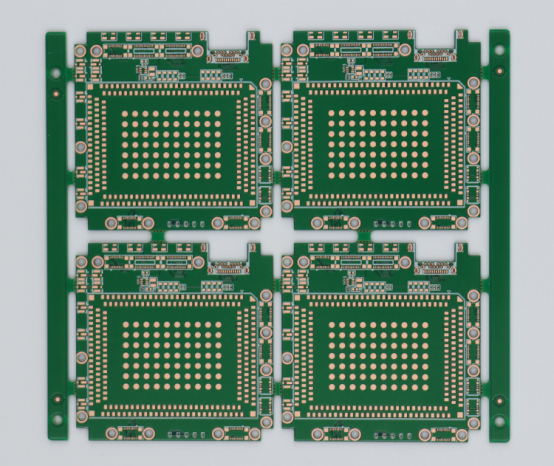
Heavy copper PCBs (printed circuit boards) are specialized boards designed to handle large currents and high-power applications. Unlike standard PCBs, which typically use 1–2oz copper layers, heavy copper PCBs feature copper layers of 3oz (105μm) or more. This extra thickness allows them to carry much higher currents without overheating, making them ideal for demanding systems like electric vehicles (EVs), renewable energy solutions, and industrial machinery.
As the demand for high-power systems continues to rise, heavy copper PCBs have become essential in ensuring performance and reliability. Their ability to manage heat, resist mechanical stress, and support high current flows makes them indispensable in today's most cutting-edge electronic devices. Let's dive deeper into the key advantages that make heavy copper PCBs critical for high-power applications.
Advantage 1: Higher Current Handling Capacity
How Thick Copper Traces Support High Current (Up to 1000A)
Copper traces in a PCB (Printed Circuit Board) act as conductors for electricity. The thickness of the copper in these traces plays a crucial role in how much electrical current can flow through without causing the PCB to overheat or fail. As the copper trace becomes thicker, it reduces the electrical resistance. This is because a thicker trace provides more space for the current to flow, making it easier for the electricity to move through the material.
When the copper is thick enough, it allows the board to handle larger currents without generating excessive heat. For example, a 3oz copper trace can handle 60A of current, while a 10oz copper trace can handle up to 250A. In comparison, a standard 1oz trace might only handle around 30A. This increased capacity helps prevent overheating and ensures safe and efficient operation in high-power applications.
Standard PCBs, with only 1–2oz copper, are not capable of handling the high currents required in power-intensive systems like electric vehicles or industrial machinery. These boards would overheat or become damaged due to their inability to handle large amounts of current over extended periods. Therefore, heavy copper PCBs with thicker copper traces are essential for high-power applications where current handling is crucial for performance and reliability.
Real-World Examples of Current Handling
1. EV Chargers (Electric Vehicle Chargers)
In high-current applications like DC fast chargers for electric vehicles (EVs), heavy copper PCBs are used to manage large currents. These chargers can deliver up to 350kW of power, requiring copper traces in the PCB to handle up to 500A.
For example, a 5oz to 10oz copper PCB is typically used in these systems to ensure efficient power transmission without overheating. These thick copper traces allow the PCB to support high currents, enabling quick charging times for EV batteries. Without heavy copper PCBs, the system would fail to perform optimally or safely under such high electrical loads.
2. Industrial Motor Drives
Heavy copper PCBs also play a critical role in industrial motor drives used in manufacturing and machinery. These systems often require high currents to operate large motors. For instance, a 10oz copper PCB can manage up to 250A, which is crucial for controlling motor power delivery. This ensures the motor runs smoothly and efficiently, even in demanding conditions.
Thicker copper allows for better heat dissipation, meaning that the motor drive operates at a lower temperature despite carrying high currents. The result is improved system reliability and reduced risk of overheating or failure.
3. Data Centers and Power Supplies
In data centers and large power distribution systems, where reliable power supply is crucial, 20oz copper PCBs are used to manage extremely high currents, sometimes up to 1000A. These applications require large, high-capacity copper traces to ensure that the current flows safely and efficiently across the power grid or server network.
For example, power distribution systems in data centers rely on heavy copper PCBs to distribute high current reliably across multiple racks or servers without risk of overheating. These PCBs are engineered to handle the massive power loads required to keep the servers running 24/7, ensuring maximum uptime and preventing costly system failures.
Advantage 2: Superior Thermal Management
Copper’s Thermal Conductivity and Heat Dissipation
Copper is known for its high thermal conductivity, which means it is excellent at conducting heat. The thermal conductivity of copper is 401 W/m·K, making it one of the best materials for heat dissipation. In practical terms, this means copper can transfer heat away from hot components on a PCB (Printed Circuit Board) very efficiently. This is especially important in high-power applications like electric vehicles, industrial machinery, and solar inverters, where excess heat can damage sensitive components.
In these high-power systems, excessive heat is a constant challenge. If heat isn't managed well, it can cause parts to overheat, which reduces their lifespan or causes them to fail. Copper’s ability to spread heat effectively prevents this. It acts as an effective heat sink, absorbing and distributing the heat across a larger area, which lowers the risk of overheating and ensures better performance and long-term reliability for the system.
The Science Behind Copper’s Heat Dissipation Ability
The science behind copper’s excellent heat dissipation ability lies in its atomic structure. Copper's free electrons move easily, which allows heat to spread quickly throughout the material. This makes copper an ideal choice for applications where heat needs to be spread away from sensitive parts, like power transistors, capacitors, and ICs (Integrated Circuits).
In high-power applications, where components generate a lot of heat, copper traces and copper planes help to manage the heat load. They absorb the heat produced by the electrical components and then disperse it across the PCB. Without such heat dissipation, components would quickly overheat, leading to potential failure. This is why heavy copper PCBs, with thicker copper traces (3oz–20oz), are essential for preventing thermal damage in high-power electronics.
Impact on Reducing Temperature Rise and Improving Reliability
One of the most important benefits of heavy copper PCBs is their ability to reduce temperature rise. The thicker the copper, the better it is at absorbing and distributing heat, which prevents hot spots where heat can concentrate and damage components.
For example, when comparing 5oz copper PCBs to 1oz copper PCBs, the 5oz copper design can reduce the temperature rise by 20–30°C. This might not sound like much, but even a small reduction in temperature can significantly increase the lifetime and reliability of sensitive components.
Case Study: 250W Solar Inverter
Consider a solar inverter using 5oz copper PCBs. In this case, the 5oz copper PCB runs 15°C cooler than an equivalent design using 1oz copper. This temperature reduction helps improve the longevity of components like capacitors, which are sensitive to high temperatures. The cooler operating temperature results in lower wear and tear on the system, meaning it performs better over time and requires less maintenance.
System Stability: How Improved Thermal Management Leads to Reduced Stress on Components
Improved thermal management is directly linked to system stability. When components stay cooler, they are under less stress. Heat can cause components to expand and contract, leading to mechanical stress that can wear them out more quickly. By keeping the system cooler, heavy copper PCBs reduce this stress and increase the overall lifespan of the system.
For instance, in electric vehicle powertrains and high-power industrial systems, reliable thermal management ensures that critical parts like motors, power converters, and batteries operate in the ideal temperature range. This not only improves performance but also prevents failures that can occur due to excessive heat, such as thermal runaway in batteries.
By improving thermal dissipation with copper's high thermal conductivity, the system is less prone to overheating, and components can operate within their safe temperature limits. This leads to improved reliability and longer operational life, which is critical for industries that rely on continuous operation and minimal downtime.
Advantage 3: Enhanced Mechanical Durability
Resistance to Vibration, Thermal Cycling, and Physical Stress
Heavy copper PCBs are designed to endure harsh environments where mechanical stress, vibrations, and extreme temperature changes are common. The thick copper used in these PCBs provides enhanced durability compared to standard PCBs with thinner copper traces.
Vibration Resistance: One of the key benefits of thick copper is its ability to withstand vibrations. 3oz copper traces can handle up to 20G of vibration (according to MIL-STD-883H, a military standard), while standard 1oz copper traces can only resist 10G. This makes heavy copper PCBs ideal for applications in environments with constant movement or vibrations, such as automotive and aerospace systems. The thick copper in these PCBs absorbs and distributes the mechanical stress from vibrations, ensuring that the components remain intact and function reliably.
Thermal Cycling Resistance: Heavy copper PCBs are also resistant to thermal cycling, which refers to the expansion and contraction of materials as temperatures change. In applications where temperatures fluctuate drastically (such as between -40°C to 125°C), heavy copper PCBs can endure over 1000 thermal cycles with minimal degradation. This resistance is essential for the longevity and reliability of systems that experience extreme temperature variations, like automotive powertrains or aerospace systems. The thick copper traces help the PCB maintain structural integrity and performance despite the constant thermal stress.
Physical Stress Resistance: Thick copper pads and traces also provide better resistance to physical stress, such as damage from repeated connector insertions or mechanical handling. In systems where the PCB is subjected to frequent physical contact, such as in industrial machinery or automotive power systems, the thick copper ensures the pads and traces remain intact and resistant to cracking or wear. This enhances the overall durability of the PCB, reducing the need for repairs or replacements in rugged environments.
Applications in Harsh Environments
Heavy copper PCBs are especially beneficial in industries and applications where the equipment is exposed to harsh environments. Below are two key areas where the enhanced mechanical durability of heavy copper PCBs plays a critical role:
Aerospace: Aerospace systems are subject to extreme conditions, including high vibrations, temperature fluctuations, and physical stresses during takeoff, flight, and landing. For example, aerospace PCBs are used in navigation systems, flight control systems, and power management circuits, where reliability is critical. The thick copper in these PCBs ensures that they can survive the constant mechanical and thermal stress of flight, maintaining their performance without cracking or failing. The vibration resistance and thermal cycling resistance of heavy copper PCBs are vital for the durability of these systems in the challenging aerospace environment.
Automotive: In automotive applications, heavy copper PCBs are used in powertrains, battery management systems (BMS), and electric vehicle systems. These systems are subjected to vibrations, temperature changes, and physical stresses from road conditions and engine operation. Heavy copper ensures that the PCBs can endure these stresses while maintaining reliable performance. For instance, electric vehicle (EV) battery management systems require high current handling and thermal management, making heavy copper PCBs essential for safely distributing power and maintaining system stability over time. Similarly, automotive powertrains rely on durable PCBs to manage the high currents and extreme conditions that can lead to PCB damage in standard designs.
Advantage 4: Miniaturization and Design Flexibility
Smaller Trace Sizes Due to High Current Capacity
One of the most significant advantages of heavy copper PCBs is their ability to carry higher currents without increasing the width of the copper traces. This means that narrower traces can be used in the PCB design, allowing for more compact and efficient designs. The thicker the copper, the more current it can handle without overheating or failing. This is especially useful for applications where space is limited, but high current capacity is still required.
For example, consider a circuit that needs to carry 60A of current. With a standard 1oz copper PCB, the trace width required to handle this current is about 10mm. However, with 3oz copper (a heavier copper thickness), the same current can be handled with a 5mm-wide trace, effectively saving 50% of space. This reduction in trace width allows for smaller, more efficient PCB designs, which is essential for applications where every millimeter of space counts, such as in compact consumer electronics, automotive systems, and renewable energy devices.
Benefits in Reducing PCB Size for Compact Device Designs
Heavy copper PCBs enable more efficient designs by allowing narrower traces, which results in smaller PCBs without sacrificing performance. This is particularly beneficial in devices that require high power in a compact form factor, such as electric vehicle (EV) on-board chargers, industrial robots, and renewable energy equipment. In these devices, space is limited, but the need for high current handling and reliable performance is crucial. Heavy copper makes it possible to meet both needs.
For example, in an EV on-board charger, heavy copper PCBs enable smaller circuit boards that can handle the high current required for fast charging while maintaining a compact size. This is critical for integrating the charger into the small space available within the vehicle. Similarly, industrial robots that require high power to operate efficiently can benefit from heavy copper PCBs, allowing the power electronics to fit into a smaller, more streamlined design while still performing at high levels.
By enabling miniaturization without compromising power handling capabilities, heavy copper PCBs open up new possibilities for designing portable and space-constrained devices. This is especially important in consumer electronics, where smaller, lightweight devices are in high demand. For example, smartphones or wearable devices can benefit from the ability to pack more power into a smaller space, improving both performance and battery life.
The Role of Heavy Copper in Space-Constrained Applications
Heavy copper's ability to reduce the size of PCBs without sacrificing current-carrying capacity is a game-changer for devices that need to fit into tight spaces while still offering high performance. In renewable energy applications, for example, solar inverters and wind turbine controllers can be made more compact using heavy copper, allowing for easier installation in space-limited environments without compromising the power conversion efficiency.
In consumer electronics, where space constraints are always a challenge, heavy copper PCBs allow designers to create smaller, more powerful devices without overheating issues. This could lead to the development of more energy-efficient products with higher performance and longer operational life, as thermal and mechanical stress are better managed in smaller designs.
Conclusion
In conclusion, heavy copper PCBs offer significant advantages for high-power systems. They provide increased current handling, allowing circuits to carry much larger currents without overheating. Their superior thermal management helps dissipate heat more effectively, ensuring reliable operation. The enhanced mechanical durability of heavy copper PCBs makes them resistant to vibration, thermal cycling, and physical stress, making them ideal for demanding environments. Furthermore, their ability to support narrower trace sizes leads to more compact and efficient designs, enabling smaller devices without sacrificing performance.
These advantages are transforming industries like electric vehicles, renewable energy, and industrial automation, where the demand for high-power, reliable, and space-efficient systems is growing rapidly. As the power densities in next-generation technologies continue to rise—such as in 800V EVs or 1MW solar inverters—the need for heavy copper PCBs will only increase. These advanced PCBs will continue to play a crucial role in enabling efficient, high-performance designs for the technologies of tomorrow.
At PCBMASTER, we specialize in producing high-quality heavy copper PCBs tailored to your specific needs. Whether you're designing complex power systems for industrial machinery or cutting-edge electric vehicles, we provide the precision and durability required to power the next generation of electronic devices.
FAQs
1. Why is thermal management so important in high-power PCBs?
Thermal management is critical in high-power PCBs because as electrical current flows through the traces, it generates heat. Without proper heat dissipation, components can overheat, leading to failure or reduced lifespan. Heavy copper PCBs help manage this issue due to copper's high thermal conductivity, which allows heat to spread quickly and evenly across the PCB. This helps prevent hot spots and ensures the reliability and longevity of the system.
2. How do heavy copper PCBs contribute to the miniaturization of electronic devices?
Heavy copper PCBs allow for narrower traces while still handling higher currents. This means that designers can use smaller PCB layouts without sacrificing performance, which is especially important for compact electronic devices. For example, in electric vehicle chargers or smart grid systems, the use of heavy copper allows for more efficient use of space, enabling designers to build smaller, more powerful devices.
3. Can heavy copper PCBs be used in renewable energy systems like solar inverters?
Yes, heavy copper PCBs are ideal for renewable energy applications, such as solar inverters and wind turbine controllers. These systems require high current handling and effective thermal management due to the large amounts of power they process. Heavy copper PCBs can handle high currents, prevent overheating, and provide the durability needed for long-term performance in harsh outdoor environments, making them essential for renewable energy infrastructure.

