


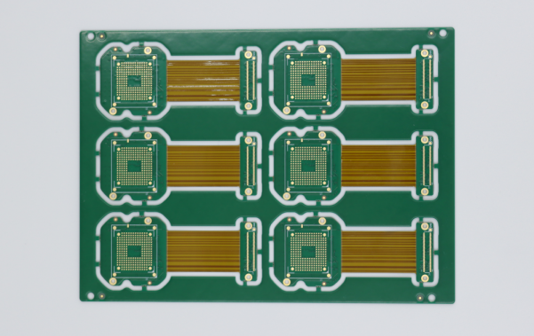
Rigid-Flex PCB Design & Manufacturing Solutions by PCBMASTER
As a high-tech enterprise specializing in precision PCB R&D and manufacturing, PCBMASTER has always been driven by technology and empowered by quality. We focus on Rigid-Flex PCBs and provide high-reliability, customized solutions for industries such as communications, consumer electronics, and industrial control.
Leveraging deep expertise in material properties, precise design optimization, and refined production management, we ensure that each PCB meets the highest standards of performance and reliability.
This guide comprehensively explains our Rigid-Flex PCB technical system across six dimensions: process flow, material selection, material properties, design key points, production control, and quality inspection.
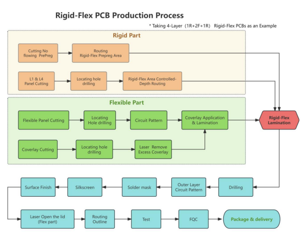
Core Production Process of Rigid-Flex PCB
PCBMASTER’s Rigid-Flex PCB production ensures high precision, stable performance, and full-process control from material preparation to final delivery. Taking a 4-layer (1R+2F+1R) rigid-flex PCB as an example, the standardized production process includes the following stages:
1. Material Preparation
l Flexible Material Cutting
l Coverlay Cutting
l NF PP (Non-Flow Prepreg) Cutting
l L1 & L4 Substrate Cutting
2. Pre-Processing
l Pre-Routing of Rigid-Flex Bonding Area
l Drilling/Punching of Locating Holes (synchronously for substrate, coverlay, and NF PP)
l Depth-Controlled Routing of Rigid-Flex Bonding Area (ensures precise bonding)
3. Inner Layer Fabrication
l Inner Layer Pattern Fabrication
l Punching of Excess Coverlay
l Rigid-Flex Integrated Lamination
l Inner Layer Pattern Etching
4. Through-Hole and Plating
l PTH (Plated Through Hole) & Panel Plating
l Through-Hole Drilling
l Coverlay Lamination
5. Outer Layer Fabrication
l Outer Layer Pattern Fabrication
l Coverlay Pressing
l Solder Mask (Green Oil) Coating
l Surface Finish (customized on demand)
l Outer Layer Pattern Etching
l Secondary Depth-Controlled Routing of Rigid-Flex Bonding Area
6. Final Processing & Testing
l Outline Routing
l Electrical Performance Test (E-Test)
l Final Quality Check (Full-Item Review)
l Vacuum Packaging & Delivery
Core Material Description and Selection Standards
Materials are the foundation of product quality. PCBMASTER follows the principle of “strict qualification access, full inspection before entry” to ensure only high-quality materials are used.
1. Substrates: Precise Matching by Performance Requirements
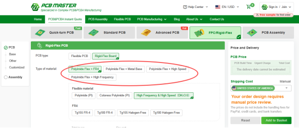
As the carrier of circuits, substrates directly influence high-temperature resistance, electrical performance, and mechanical strength. PCBMASTER offers multiple material combinations for Rigid-Flex PCBs, carefully selected based on application needs:
l Polyimide Flex + FR4 – Standard combination for balanced performance and cost.
l Polyimide Flex + Metal Base – High thermal conductivity for power-intensive applications.
l Polyimide Flex + High Speed – Optimized for high-speed signal transmission.
l Polyimide Flex + High Frequency – Ideal for RF and microwave applications.
1.1 Rigid Section:
To achieve reliability, thermal stability, and excellent signal integrity in the rigid sections of Rigid-Flex PCBs, high-quality rigid substrates are employed. The main rigid material categories include:
As the most commonly used substrate for rigid sections, PCBMASTER utilizes Tg155 FR-4, Tg180 FR-4, Tg155 Halogen-Free, and Tg180 Halogen-Free, all supplied by SYTECH. These FR-4 materials offer excellent heat resistance, CAF resistance (Conductive Anodic Filament resistance), lead-free compatibility, and outstanding through-hole reliability, delivering high cost-performance and wide adoption by customers.
Metal Base
Aluminum Base PCBs and Copper Base PCBs are used when high current carrying capacity, efficient heat dissipation, and structural stability are required. For instance, copper base PCBs can achieve thermal conductivity as high as 380 W/m·K, making them ideal for power-intensive applications.
High-Frequency & High-Speed Materials
High-frequency and high-speed substrates are characterized by a low and stable dielectric constant (Dk: 2.0–3.5), extremely low dissipation factor (Df ≤ 0.005), and excellent thermal stability. High-frequency and high-speed circuits often consume significant power, so substrates must maintain stable Dk and Df across a wide temperature range (-55℃ to 125℃) to prevent impedance drift. Common options include PTFE (Polytetrafluoroethylene), hydrocarbon ceramic substrates, and modified FR-4 substrates, supplied by Rogers, Panasonic, ISOLA, TUC, SYTECH, and others. Detailed parameters and characteristics of these materials will be covered in a dedicated article.
1.2 Flexible Section: Our company mainly selects three types of substrates
High-quality flexible substrates are used to ensure excellent signal integrity, mechanical reliability, and high-temperature performance for FPC and Rigid-Flex PCB applications. The main types of flexible substrates are:
Polyimide (PI)
PI is the core substrate for flexible printed circuits (FPC). It features solder dip resistance up to 260℃/20 sec, high dielectric strength, and excellent mechanical properties, making it suitable for high-temperature applications. PI is moisture-absorbent, so all incoming materials are stored in a constant temperature and humidity environment (humidity ≤40%) to maintain stability.
Colorless Polyimide (CPI)
Compared to traditional polyimide, CPI offers superior properties including good optical performance, low dielectric constant, excellent thermal stability, and outstanding mechanical strength. It is widely used in high-end applications such as microelectronics and optoelectronic devices, including:
l Optoelectronic packaging materials and second-order nonlinear optical materials
l Film alignment in LCD displays
l Flexible cover sheets for OLED devices
l Flexible optoelectronic devices such as flexible displays and FPCs
High-Frequency & High-Speed Flexible Substrate
This type of substrate features low dielectric constant (Dk 3.3 at 10GHz) and extremely low dissipation factor (Df 0.002 at 10GHz), ensuring minimal signal loss. It also exhibits excellent heat resistance, dimensional stability, chemical resistance, and electrical performance, is halogen-free, and meets UL94 VTM-0 flame retardancy standards. It is used for products with extremely high signal transmission requirements, such as:
l Mobile phone antennas
l Microwave communication equipment
l High-speed network devices
l Sensors
l High-frequency circuit boards
For reference, PCBMASTER uses SF701 high-frequency & high-speed flexible substrate supplied by SYTECH, with detailed performance indicators available for customers.
| Items | Test Method | Condition | Unit | Typical Value |
|---|---|---|---|---|
| Peel Strength (90°) | IPC-TM-650 2.4.9D | Accepted | N/mm | 1.0 |
| 288℃, 5s | 1.0 | |||
| Solder Resistance | IPC-TM-650 2.4.13.F | 288℃, 10s | - | No delamination |
| Dimensional Stability | IPC-TM-650 2.2.4B | After Etched | % | -0.0391/-0.0512 |
| Chemical Resistance | IPC-TM-650 2.3.2G | After Chemical Exposure | % | 97 |
| Electric Strength | IPC-TM-650 2.5.6.2A | D-48/50+D-0.5/23 | KV/mm | 159 |
| Volume Resistivity | IPC-TM-650 2.5.17E | C-96/35/90 | MΩ-cm | 1.5×10⁹ |
| Surface Resistance | IPC-TM-650 2.5.17E | C-96/35/90 | MΩ | 5.8×10⁵ |
| Dielectric Constant (10GHz) | SPDR | C-24/23/50 | - | 3.3 |
| Dissipation Factor (10GHz) | SPDR | C-24/23/50 | - | 0.002 |
| Folding Endurance | JIS C-6471 | R0.8×4.9N | Times | >400 |
| Flammability | UL94 | E-24/125 | Rating | VTM-0 |
Remarks:
l Certified to IPC-4204/24 Copper Clad Liquid Crystal Polymer Adhesiveless.
l All the typical values listed above are for your reference only; please consult the PCBMASTER team for detailed information.
2. Coverlay: Equivalent to Solder Mask Function of Rigid Boards
Coverlay in rigid-flex PCBs consists of PI substrate and adhesive, performing the core functions of insulation and solder masking, similar to the solder mask on rigid boards. Its selection is based on board thickness, copper thickness, and flexibility requirements:
l PI Substrate Thickness: Typically 12.5μm, 25μm, or 50μm. The adhesive layer is matched to the copper thickness and only fills the copper gaps after etching to prevent poor adhesion.
l High-Flexibility Applications: For components that undergo frequent bending, such as foldable screens, a 12.5μm thin PI coverlay is preferred to ensure repeated flexing reliability.
3. Adhesive Materials: Ensuring Interlayer Bonding Strength
Adhesive materials are essential for rigid-flex PCBs, providing strong interlayer bonding and maintaining dimensional stability. The main types used in different lamination scenarios are:
NF PP (Non-Flow Prepreg)
NF PP is composed of epoxy resin, glass cloth, and fillers, offering low adhesive bleed. It is suitable for selective lamination of rigid-flex boards and applications requiring high glass transition temperature (TG). For improved thermal stability and reduced Z-axis expansion, NF PP with TG ≥150℃ is employed.
Pure Adhesive (Acrylic Adhesive)
Pure adhesive, typically acrylic-based, has TG ≤100℃ and excellent flexibility. It is used only for multi-layer flexible boards. Due to its high thermal expansion coefficient, it is strictly prohibited in rigid areas to avoid interlayer cracking.
4. Stiffener: Enhancing Local Structural Strength
Stiffeners are used to reinforce soldering or mounting areas of FPC, with material selection tailored to specific scenarios:
PET Stiffener
PET stiffeners are applied in areas without soldering requirements, offering lightweight construction and moderate cost.
PI Stiffener
PI stiffeners are the preferred choice for soldering areas, providing high-temperature resistance compatible with soldering processes. They are bonded using thermosensitive adhesive (TSA), with adhesion strength ≥1.2 N/mm.
FR-4 Stiffener
FR-4 stiffeners are used for thick boards (≥2.0 mm) or high-load-bearing areas. They are bonded with pressure-sensitive adhesive (PSA) to ensure mounting stability.
Metal-Based Stiffeners
l Stainless Steel Sheet: Thickness 0.1–0.5 mm, ultra-high rigidity (tensile strength > 500 MPa) and provides electromagnetic shielding.
l Aluminum Alloy Sheet: Thickness 0.1–2.0 mm, high thermal conductivity (130 W/m·K) and lightweight, ideal for heat dissipation and structural support.
Key Material Properties and Application Specifications
PCBMASTER strictly follows international standards such as IPC-4101 and IPC-6013 to ensure precise matching between material properties and product requirements. The main material categories are:
1. Dielectric Materials (Prepregs)
Prepregs, mainly non-flow or low-flow types, are used to bond rigid layers.
High-TG Prepreg:
High-TG prepregs are designed for demanding applications, offering excellent thermal and mechanical performance. They can withstand high operating temperatures while maintaining dimensional stability. Their low Z-axis coefficient of thermal expansion (≤50 ppm/℃) helps improve through-hole plating reliability and reduces the risk of delamination. These properties make them ideal for use in industrial control products, where long-term reliability and precision are critical.
Design Notes:
High-TG prepregs have a relatively low dielectric strength (≤40 kV/mm), which means that the thickness of the dielectric layer should be increased during design to compensate and ensure reliable electrical performance. In addition, the specific application areas of these materials must be clearly indicated in design drawings to prevent misapplication and ensure that the material is used correctly within the PCB structure.
2. Flexible Adhesive Film
Flexible adhesive films are used to bond multi-layer flexible layers and provide structural support. Core properties include high bonding strength and low TG.
l Formulated with resin TG ≤80℃ to improve adhesion to PI substrate (adhesion ≥1.0 N/mm) and maintain flexibility
l Prohibited in rigid areas: High Z-axis expansion (≥80 ppm/℃) may cause interlayer delamination. PCBMASTER includes a design review check to prevent misuse
3. Flexible Copper Clad Laminate (FCCL)
FCCL is divided into adhesiveless and adhesive-based types, selected based on layer count and temperature requirements:
l Adhesiveless FCCL: PI dielectric is directly coated or deposited on metal foil, avoiding low-TG adhesive. Suitable for rigid-flex boards with ≥8 layers and high-temperature scenarios (≥125℃). PCBMASTER uses this type for all high-layer boards.
l Adhesive-Based FCCL: Used for boards with ≤4 layers and room-temperature scenarios to avoid adhesive failure (TG ≤90℃) at high temperatures
Key Engineering Design Considerations
Based on experience from thousands of projects, three principles guide rigid-flex PCB design: error prevention, efficiency improvement, and reliability guarantee.
1. Expansion-Contraction Control: Ensuring Lamination Precision
Composite materials such as FPC, FR-4, and NF PP can expand or contract differently during lamination, posing a major challenge. PCBMASTER addresses this through a dual-dimension design approach:
l Rivet Hole Count: 8 holes are placed uniformly on the board edges (2 per side) to form a symmetrical positioning system, offsetting expansion-contraction stress.
l Rivet Hole Configuration:
- Rigid Board Holes: CNC-drilled with a 3.20 mm drill bit (compatible with 3.175 mm rivets)
- FPC Holes: Copper layer retained at punching position (copper thickness ≥1 oz) to strengthen hole walls and prevent chipping or misalignment (misalignment tolerance ≤0.05 mm)
2. FPC Circuit Pattern Design: Balancing Electrical and Mechanical Performance
Circuit pattern design should minimize stress concentration and signal loss, following standardized guidelines.
l Circuit Transition: Avoid abrupt changes in width or thickness. Use a teardrop transition at thickness changes with a minimum angle of 135° to prevent circuit fractures during bending.
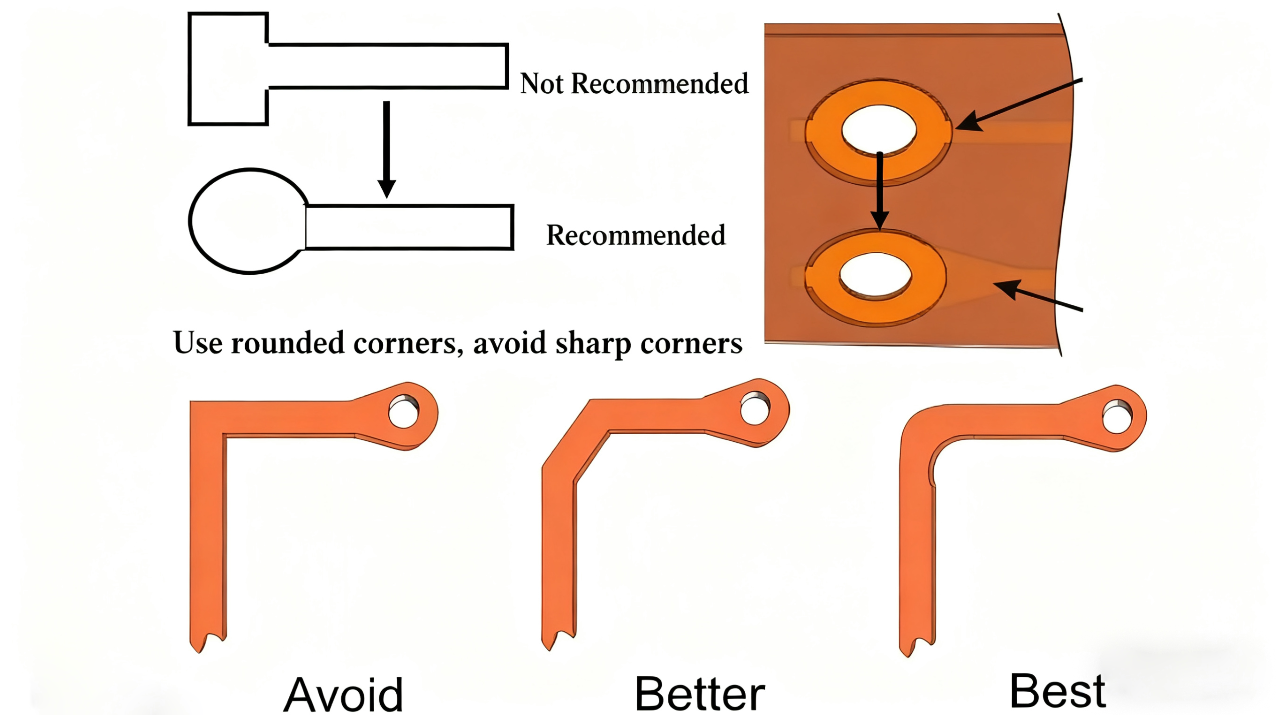
l Pad Design: Use the largest pad size that meets electrical requirements (minimum diameter ≥0.8 mm). Apply an arc transition at the connection between pad and trace (radius ≥0.1 mm) to prevent right-angle discharge.
l Copper Layer Optimization: Use solid copper in scrap areas with a copper ratio of at least 70%. This improves board flatness and reduces etching deformation.
l Special Design for Flexing Areas:
a. Orient the copper layer perpendicular to the bending direction, ensuring uniform coverage across the entire flexing area.
b. Avoid via holes or plated through holes (PTH) to prevent hole wall cracking.
c. Layer Count Control: Limit the number of layers in the flexing area to 2 or fewer to reduce flexing stress.
d. Rolled Copper Selection: Align the copper lattice direction with the bending direction to enable over 100,000 bending cycles at 180°.
e. Edge Reinforcement: Add 0.2 mm-wide copper strips at the edges of flexing areas without large copper foil traces to prevent delamination.
3. Distance and Opening Design: Ensuring Lamination and Insulation Reliability
l Hole-to-Edge Distance: Maintain a minimum distance of 0.5 mm from the outline edge of the flexible or rigid area to the inner hole edge. Include positioning tolerance (±0.03 mm) and processing tolerance (±0.02 mm).
l PTH-to-Edge Distance: Ensure a minimum distance of 0.6 mm from plated through holes (PTH) in the rigid-flex bonding area to the edge of clearance holes. This prevents adhesive bleed from blocking through holes during lamination.
l Coverlay Opening: Create openings on the fabrication edge and board edge to enhance rigid-flex bonding. In flexible areas, the coverlay extends 0.4 mm into the rigid board on one side, and the gap between PTH and the coverlay should be ≥0.5 mm to prevent green solder mask infiltration.
l NF PP Opening: Retract the NF PP used for lamination in the rigid board by 0.25 mm from the board edge to avoid adhesive bleed contaminating the flexible area.
Key Points of Refined Production Process Control
PCBMASTER has established a production management system of "process-specific control and full-process traceability". The control standards for core links are as follows:
1. Cutting: Eliminating Interlayer Bonding Risks
l Direct cutting of single-sided boards is strictly prohibited for rigid boards and FPC. For double-sided boards, etch to single-sided while controlling copper thickness deviation within ±10% to ensure interlayer bonding strength and prevent board explosion or delamination.
l Maintain cutting dimension tolerance within ±0.1 mm to guarantee precision for subsequent lamination.
2. Inner Layer Circuit: Ensuring Pattern Integrity
l Incoming Inspection: FPC must be flat, without creases or adhesive stains. Rejection rate should not exceed 0.1%.
l Developing and Etching: Each FPC must be attached to a dedicated carrier board (1 carrier board per board) to prevent folding during conveyance. Line width tolerance after etching should be within ±0.02 mm.
l Inspection Requirements: 100% of all boards undergo Automatic Optical Inspection (AOI). Wire repair is prohibited for FPC; defective boards are directly scrapped.
3. Lamination: Dedicated Program + Strict Inspection
l Dedicated Program: Use the dedicated lamination program (internal number #535) for rigid-flex boards. Mixed lamination is strictly prohibited. The lamination temperature profile is controlled in three stages: Heating → Constant Temperature → Cooling. Constant temperature is 180±5℃, maintained for 90±5 minutes.
l Riveting Control:
a. FPC Brown Oxidation: Attach a carrier board for processing. Any wrinkles after brown oxidation result in immediate scrapping.
b. NF PP Storage: Store in a dehumidifying cabinet (humidity ≤30%) for at least 12 hours to prevent moisture absorption.
c. Lamination Inspection: After riveting, manually check the number of prepregs (no missing or excess prepregs), then use X-ray to inspect layer alignment. Layer misalignment tolerance ≤0.03 mm.
l Lamination Auxiliary: Cover the riveted boards with 1.0 mm-thick silicone rubber on both top and bottom. Stack 6 layers per box to ensure sufficient resin filling without bubbles or voids.
4. Drilling and PTH & Plating
l Drilling: Use MO (Molybdenum Steel) drill bits with Vigor drilling machines. Focus on the T-joint area of the rigid-flex bond on the flexible board. Residual adhesive or burrs must not exceed 0.01 mm in height. Drilling parameters are adjusted immediately if abnormalities are detected.
l PTH & Plating:
a. Desmear: Use a dedicated program for rigid-flex boards to avoid damage to the PI substrate.
b. PI Adjustment: Maintain chemical concentration at 40% (volume ratio), temperature at 40±2℃, for 4–8 minutes.
c. PTH Inspection: Backlight inspection grade must be ≥9.5 to ensure 100% hole wall coverage.
d. Panel Plating: Copper thickness must be ≥20 μm, with uniformity deviation ≤10%.
5. Cover Opening Technology: Customized by FR-4 Core Insulation Thickness
Cover opening is a core process for rigid-flex boards. Our company selects differentiated schemes according to the FR-4 core insulation thickness (d):
5.1 1R+2F+1R Structure
l Basic Scheme: Use blind routing with depth-controlled butt-joint technology (typical board thickness 1.60 mm). Control the blind slot depth on the FR-4 inner layer before lamination (retain 1/2 residual thickness) and perform cover opening with secondary depth control after lamination.
l Thickness Adaptation:
d ≤0.40 mm: Dual laser blind slot depth control (laser power 15±2 W) to prevent mechanical damage to the flexible board.
d >0.40 mm: For regular straight bonding areas, use “first blind routing + later V-CUT” (V-CUT angle 45±5°) to improve efficiency. For irregular bonding areas, use dual blind routing depth control to ensure outline precision.
5.2 2F+2R Structure
FPC and rigid boards are directly laminated. To ensure circuit reliability, use a combined scheme of laser blind cutting (primary) + routing/V-CUT depth control (secondary). Depth deviation of laser blind cutting must be ≤0.02 mm to avoid copper exposure.
Comprehensive Quality Inspection Standards
PCBMASTER has established a full-process inspection system covering four main categories and 18 inspection items. All products must pass strict inspections before delivery.
1. Inspection Basis
Aligned with international authoritative specifications:
l IPC-A-600: Acceptability of Printed Circuit Boards, used for appearance and dimension evaluation.
l IPC-6012: Qualification and performance specification for rigid printed boards, used for evaluating rigid section performance.
l IPC-6013: Qualification and performance specification for flexible printed boards, used for evaluating flexible section performance.
2. Four Categories of Inspection Items
2.1 Electrical Performance Test
l E-Test: 100% continuity test (≤50 mΩ) and insulation resistance test (≥10^10 Ω at 500 V DC).
l Impedance Test: Customized per customer requirements (±10% deviation); high-frequency products also require insertion loss testing (≤0.5 dB/m @1 GHz).
2.2 Dimensional Precision Test
l Inspection Items: Outline dimensions (±0.1 mm), board thickness (±0.05 mm), hole diameter (±0.02 mm), line width (±0.02 mm), annular ring width (≥0.15 mm), plating thickness (Cu ≥20 μm, Ni ≥5 μm, Au ≥0.8 μm), board warpage (rigid ≤0.75%).
l Inspection Equipment: 2D image measuring instrument (precision ±0.001 mm), plating thickness gauge.
2.3 Appearance Quality Test
l Visual Inspection: No scratches (≤0.01 mm), bubbles (≤0.2 mm diameter, max 2 per board), adhesive stains, or copper exposure.
l Adhesion Test: Solder mask adhesion (100/100 cross-cut test, no peeling), coverlay/stiffener peel strength (≥1.0 N/mm).
2.4 Reliability Test
l Solderability: Solder dip at 260℃ for 5 sec, wettability ≥95%.
l Thermal Shock: -40℃ → 125℃, 30 min each, 100 cycles, no cracking or delamination.
l Flexibility: 180° bending (1 mm radius), normal circuit continuity after 100,000 cycles.
l Other Items: Ion contamination ≤1.5 μg NaCl/cm², moisture and insulation (≥10^9 Ω after 1000h at 85℃/85% RH), cross-section inspection (no interlayer bubbles, no hole wall voids).
Conclusion
PCBMASTER has always been customer demand-oriented, with technological innovation at its core, and continues to deepen its presence in the rigid-flex PCB field. From material selection and engineering design to production control and quality inspection, every step reflects our commitment to precision and reliability.
We provide comprehensive Electronics Manufacturing Services, including PCB Prototype, Quick-turn PCB, Standard PCB, Advanced PCB, FPC/Rigid-Flex, High Frequency & High Speed PCB, Metal Base PCB, Alumina & AN Ceramic PCB, and PCB Assembly. Our solutions help customers’ products excel in high-precision, high-reliability, and high-stability applications.
FAQs
1. What makes Rigid-Flex PCBs suitable for compact and complex electronic designs?
Rigid-Flex PCBs combine rigid layers with flexible circuits in a single board, allowing designers to create compact, multi-dimensional layouts. This reduces the need for connectors and interconnecting cables, making devices lighter and more reliable.
2. How do manufacturers ensure strong bonding between the rigid and flexible sections?
Manufacturers use precise adhesives like NF PP (Non-Flow Prepreg) or acrylic adhesives, control lamination temperatures and pressure carefully, and perform inspections like X-ray layer alignment checks. This ensures the rigid and flexible sections remain securely bonded during use.
3. In what applications are Rigid-Flex PCBs most commonly used?
Rigid-Flex PCBs are widely used in aerospace, automotive, medical devices, industrial control, and consumer electronics. They are ideal for products that require tight space utilization, repeated bending, or high reliability under mechanical stress.

