


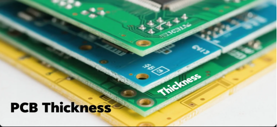
Essential Guide to PCB Thickness Choosing the Right Specifications
Introduction
In electronic device design, a PCB (Printed Circuit Board) acts like an “electronic skeleton,” supporting all components and enabling circuit connections. Printed circuit boards come in a variety of thicknesses depending on their application. However, while designers often focus on PCB layer count and material, they can easily overlook a key parameter—thickness.
You might ask, “Isn’t it just about how thick the board is? Isn’t choosing the most common 1.6mm enough?” Actually, no. Circuit board thickness is more than just a single standard value; it is influenced by design requirements, application, and industry standards. The 1.6mm value is the typical PCB thickness used in most applications, but other thicknesses are also common depending on specific performance or mechanical requirements. PCB thickness directly affects a device’s portability, heat dissipation capability, mechanical strength, and even manufacturing cost. For instance, a smartwatch PCB needs to be as thin as 0.4mm to fit into a compact casing, while an industrial control cabinet PCB might require a thickness of 2.4mm or more to withstand mechanical shock.
This article will use simple language to give you a comprehensive understanding of the secrets behind PCB thickness: from common thickness specifications and selection criteria to practical case studies for different scenarios. It will help you avoid the pitfalls of “wasting money if too thick” or “failing if too thin,” while mastering techniques to optimize design and cost.
Introduction: What is a PCB and Why Does Thickness Matter?
A Printed Circuit Board (PCB) is the foundation of nearly every modern electronic device, from smartphones and laptops to industrial machinery and medical equipment. Acting as the central platform, a PCB connects and supports all the electronic components, ensuring that signals and power flow exactly where they’re needed. But while the layout and number of layers often get the spotlight, the thickness of a PCB is just as crucial.
Standard PCB thicknesses have become the industry norm for good reason—they strike a balance between mechanical strength, manufacturability, and compatibility with automated assembly processes. However, the right PCB thickness isn’t just about following tradition. The thickness you choose directly impacts your circuit board’s mechanical strength, thermal performance, and signal integrity. For example, a board that’s too thin might flex or break under stress, while a board that’s too thick could add unnecessary weight and cost, or even affect how signals travel across the board.
During the design process, considering PCB thickness early on helps ensure your electronic devices are reliable, robust, and cost-effective. Whether you’re working with standard PCBs or exploring custom solutions, understanding how thickness affects your printed circuit board’s performance is key to making the right choices for your application.
Understanding PCB Layer Structure
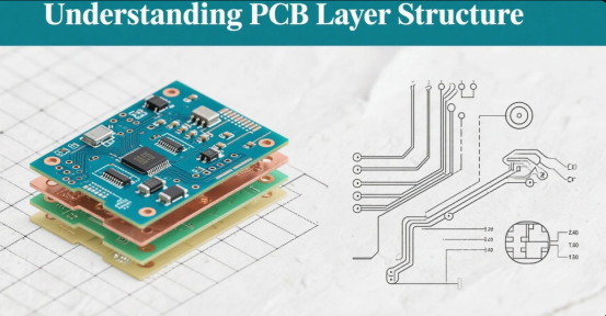
·Every PCB is built from a carefully engineered stack of layers, each serving a specific purpose in the board’s function and durability. At the heart of the board is the substrate, usually made from a dielectric material like FR4 or polyimide, which provides the mechanical backbone and determines much of the board’s thickness and rigidity.
·On top of the substrate are the copper layers, which form the electrical pathways for signals and power. The number and thickness of these copper layers can vary depending on the complexity of the circuit and the current-carrying requirements. Thicker copper layers are often used for power circuits or to improve heat dissipation, while thinner layers are common in high-density signal routing.
·Covering the copper is the solder mask, a protective coating that shields the copper from oxidation, environmental stress, and accidental solder bridges during assembly. The solder mask also plays a role in defining the board’s final thickness and helps with precise component placement by exposing only the necessary pads. Finally, the silkscreen layer adds visual indicators—like component labels and orientation marks—to guide assembly and troubleshooting.
·Understanding how these layers interact and contribute to the overall board thickness is essential for designing a PCB with the appropriate thickness for your application. Each layer, from the copper to the solder mask, must be considered to ensure optimal performance and manufacturability.
Material Selection: How Dielectrics and Substrates Influence Thickness
·The choice of materials in PCB fabrication goes far beyond aesthetics—it’s a critical factor that shapes the board’s thickness, performance, and reliability. The substrate, typically made from dielectric materials such as FR4 or polyimide, forms the core of the board and largely determines its mechanical strength and insulating properties. The thickness of this substrate, combined with the prepreg layers used in multilayer PCBs, sets the baseline for the overall thickness.
·Copper layers are then laminated onto the substrate. Opting for thicker copper layers can significantly enhance the board’s ability to carry higher currents and dissipate heat, which is especially important in power electronics or applications demanding improved heat dissipation. However, thicker copper also increases the total thickness of the PCB and can affect the etching process, so it’s important to balance electrical performance with manufacturability.
·Dielectric constant and thermal conductivity are two key properties of the materials used. A lower dielectric constant can improve signal integrity, making it ideal for high-speed or RF applications, while higher thermal conductivity helps the board dissipate heat more efficiently. Selecting the right combination of dielectric materials and copper weights ensures your PCB meets the demands of both electrical performance and mechanical strength, all while maintaining the optimal PCB thickness for your design.
First, Understand: PCB Thickness Isn’t “Choose Whatever You Want”

·While it might seem like you can simply pick any thickness for your PCB, the reality is more nuanced. The industry relies on standard PCB thicknesses—such as 1.57 mm or 2.36 mm—because they are optimized for compatibility with most components, assembly processes, and manufacturing equipment. These standard PCBs help streamline production, reduce costs, and ensure reliable performance across a wide range of applications.
·Choosing a custom PCB thickness is possible, but it comes with trade-offs. Custom thicknesses can increase material costs, complicate the manufacturing process, and may not be supported by all PCB manufacturers. Non-standard thicknesses might also require special handling during assembly or lead to longer production lead times. That’s why, unless your application has unique requirements, it’s usually best to select from the standard PCB thicknesses available. This approach ensures you get the appropriate PCB thickness for your needs while keeping your project on schedule and within budget.
Key Question: How Thick Should My PCB Be? 4 Core Criteria for Decision
Selecting the right PCB thickness is about more than just picking a number—it’s about balancing the specific needs of your application across four key criteria: thermal management, signal integrity, mechanical stability, and manufacturing constraints.
·Thermal Management: For high-power applications, thicker boards and thicker copper layers can provide better heat dissipation, helping to prevent overheating and ensuring reliable operation. Optimizing PCB thickness for thermal performance is especially important in power electronics and LED lighting.
·Signal Integrity: In high-speed or RF designs, thinner boards can help reduce signal loss and minimize crosstalk between traces, preserving signal quality. The right PCB thickness can make a significant difference in maintaining signal integrity, especially as data rates increase.
·Mechanical Stability: Applications exposed to mechanical stress—such as vibration, bending, or impact—benefit from thicker boards, which offer greater rigidity and resistance to deformation. Mechanical stability is crucial for industrial, automotive, and aerospace circuit boards.
·Manufacturing Constraints: Finally, practical considerations like production costs, lead times, and compatibility with standard assembly processes must be factored in. Thicker boards may cost more and require specialized handling, while thinner boards can be more fragile during manufacturing and assembly.
By weighing these four criteria, you can determine the appropriate thickness for your PCB—whether that means choosing thicker boards for improved heat dissipation and mechanical strength, or thinner boards for better signal integrity and compact designs. The goal is always to find the optimal PCB thickness that meets your technical requirements without compromising on manufacturability or cost.
First, Understand: Standard PCB Thickness Isn't "Choose Whatever You Want"
First, establish this understanding: PCB thickness is a parameter that combines standardization and customization; it’s not decided by a designer’s feeling. The reason standard thicknesses exist in the industry is essentially to balance “performance needs” with “manufacturing efficiency”—for example, standard thicknesses fit universal component pin lengths and assembly equipment fixtures, reducing customization costs. The standard pcb thickness serves as an industry benchmark, ensuring compatibility and reliability across most applications.
The 3 Most Common Standard Thicknesses, Used in 90% of ScenariosCurrently, the most universal pcb board thickness specifications globally are these three types, all derived from the 1.6mm benchmark. If you prioritize choosing from these three types during design, you probably won’t go wrong:
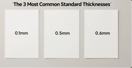
·1.6mm (Standard Version): The most mainstream thickness, equivalent to 63mil (a common imperial unit in electronics, 1mil=0.0254mm). From mobile phone motherboards and routers to household appliances, 80% of consumer electronics PCBs use this thickness. Its advantage is “balance”—it can support most components (like resistors, capacitors, IC chips) without making the device overly thick and heavy, and it fits the fixture sizes of automated assembly lines.
·2.4mm (Enhanced Version): Equivalent to 94.5mil, nearly 1.5 times the thickness of 1.6mm. Suitable for scenarios requiring higher mechanical strength, such as industrial control equipment and automotive electronics (e.g., car navigation motherboards). These devices may face environments with vibration and impact; the 2.4mm thickness reduces the risk of PCB bending and deformation. It also allows more space for copper layers, enhancing heat dissipation capability.
·3.2mm (Heavy-Duty Version): Equivalent to 125.98mil, about twice the thickness of 1.6mm. Mainly used in large equipment, such as server motherboards and medical devices (e.g., ECG machines). These PCBs often have many high-power components (like power modules) soldered on them. The 3.2mm thickness can accommodate thicker copper foil (e.g., 3oz copper, whereas standard PCBs often use 1oz) and enhances the board’s load-bearing capacity, preventing deformation over time due to component weight.
Besides these three, there are also 1.0mm (Thin Version) and 0.8mm (Ultra-Thin Version), but these belong to “non-standard common types.” They are used in extremely slim devices like smartwatches and wireless earbuds. However, you must confirm manufacturer support beforehand to avoid increased production difficulty due to special thickness. Selecting a custom thickness may be necessary for unique applications, but it often involves additional manufacturing considerations and potential cost increases.
The “Invisible Constraints” of Thickness: Manufacturing Process and Materials
Why is it not recommended to arbitrarily choose a non-standard thickness (like 1.2mm, 2.0mm)? Because pcb board thickness is determined by the combination of “substrate + copper foil + solder mask,” and the substrate (like commonly used FR-4) is produced in fixed specifications (e.g., 0.2mm, 0.4mm, 0.8mm). The choice of board material is crucial, as it influences available thickness options, mechanical properties, and compatibility with manufacturing processes. Designers need to achieve the target thickness by “stacking multiple substrate layers.”
For example: If you want a 1.6mm PCB, the manufacturer typically uses “one piece of 1.2mm FR-4 substrate + 0.2mm copper foil on each side + solder mask” layered together. If you insist on a 1.2mm thickness, it might require using “0.8mm substrate + 0.2mm copper foil,” but 0.2mm copper foil is prone to breakage during etching, increasing production yield risk—this is the core reason why non-standard thicknesses lead to higher costs.
Key Question: How Thick Should My PCB Be? 4 Core Criteria for Appropriate PCB Thickness Decision

Choosing PCB thickness shouldn’t be about “following the trend,” like choosing 1.6mm just because others do. You might end up with a device that can’t fit or doesn’t meet performance standards. The correct approach is to judge based on four dimensions: “device scenario, component requirements, mechanical environment, and cost budget.” Selecting different pcb thicknesses is essential to meet the specific electrical, mechanical, and thermal requirements of each project, ensuring optimal performance and durability. Let’s break them down one by one:
1.Device Scenario: The Primary Conflict is “Thin/Light” vs. “Thick/Heavy”
The device’s physical size directly determines the upper limit of PCB thickness—this is the most intuitive criterion:
·Portable Devices (phones, tablets, earbuds): Prioritize thin versions below 1.0mm, even ultra-thin 0.4mm boards. For example, the iPhone motherboard is about 0.8mm thick, needing to fit into a compact body and avoid conflicts with components like the battery and screen. Note: For thin PCBs, the copper foil thickness shouldn’t be too high (recommend 1oz or less), otherwise it increases board rigidity, leading to breakage when bent.
·Desktop Devices (computers, printers):
Choosing the standard 1.6mm version is sufficient. These devices are not sensitive to thickness; 1.6mm balances performance and cost while facilitating later repairs (e.g., less likely to damage the PCB during disassembly).
·Industrial/Outdoor Equipment (frequency converters, base station equipment)
Choose enhanced versions of 2.4mm or above. For example, PCBs in outdoor base stations must endure temperature changes from -30°C to 70°C. Thicker boards have a lower coefficient of thermal expansion, reducing solder joint failure caused by temperature fluctuations, and also better resist erosion from rain and dust.
2.Component Requirements: “Weight and Heat” are Key
The components soldered onto the PCB are the “invisible drivers” determining thickness, mainly based on two indicators:
·Component Weight: If the PCB has high-power power modules, connectors, or other “heavy components” (single component weight >5g), a thicker board is mandatory. For example, a DC-DC power module in industrial equipment weighs about 10g. If a 1.6mm PCB is used, prolonged use might cause the PCB to sag in the middle due to gravity, potentially breaking solder joints; switching to a 2.4mm thick board provides sufficient rigidity to avoid this issue.
·Component Heat Dissipation: High-power components (like LED driver chips, motor controllers) generate heat during operation. A thick PCB can improve heat dissipation by “increasing copper foil thickness.” For example, the PCB in a new energy vehicle charging pile needs to handle power above 200W. Choosing a 3.2mm thick board with 2oz copper foil offers 40% higher heat dissipation efficiency than a 1.6mm thin board, preventing chip shutdowns due to overheating. The pcb copper thickness directly affects the board's ability to dissipate heat efficiently.
·Integrated Circuits: The requirements of integrated circuits, such as pin density and heat output, can also influence the choice of PCB thickness to ensure proper mounting and reliable operation.
3.Mechanical Environment: Consider “Will it be bumped? Will it bend?”
If the device might face mechanical stress like vibration, impact, or squeezing, the PCB thickness must be “increased”:
·Vibration Environment (cars, drones): Continuous vibration occurs during vehicle operation (especially for PCBs near the engine). A 1.6mm thin board is prone to “fatigue fracture,” like solder joints falling off at the edges. Choosing a 2.4mm thick board and adding “stiffeners” (FR-4 material extensions) along the PCB edges enhances vibration resistance.
·Bending Scenarios (wearable devices, foldable phones): PCBs in these devices need to bend slightly, so boards that are too thick cannot be used. For example, the PCB near the hinge of a foldable phone must be controlled between 0.4mm~0.6mm and must use “flexible substrate” (like PI material). Using a 1.6mm rigid board would cause it to snap upon folding.
The mechanical properties of the substrate, including substrate thickness, play a crucial role in determining the board's strength and ability to withstand mechanical stress.
4.Cost Budget: How Much More Expensive is a Thicker Board?
Finally, cost is an unavoidable factor. Generally, for every 0.5mm increase in PCB thickness, the cost rises by 10%~20%, for two reasons:
·Material Cost: Thicker boards require more substrate and copper foil. For example, a 3.2mm PCB uses twice the substrate of a 1.6mm one, and copper foil usage increases accordingly.
·Manufacturing Difficulty: Thicker boards are more prone to defects during drilling and lamination (like drill misalignment, lamination bubbles), leading to lower yield rates. Manufacturers need to charge a “thick board processing fee.”
Example: For the same 10cm×15cm FR-4 PCB, the unit price for 1.6mm thickness is about $5 per piece, for 2.4mm about $6 per piece, and for 3.2mm about $7.5 per piece. If your device has no mandatory thickness requirements, choosing 1.6mm controls costs most effectively.
Other Considerations:
·Signal Integrity: For high-frequency designs, impedance control is a key consideration. The number of pcb layers and the overall thickness directly affect impedance, signal attenuation, and electromagnetic compatibility.
·Thermal Management: Effective thermal management is essential to protect critical components from overheating. The use of heat sinks, along with proper PCB thickness and copper thickness, helps dissipate heat and maintain reliable operation.
Practical Case Studies: PCB Thickness and Copper Thickness Selection Plans for Different Scenarios

Theory alone isn’t enough. Here are 3 case studies for common scenarios to help you visually understand how to choose thickness:
Case 1: Consumer Electronics — Smart Speaker PCB
·Requirements: Size 12cm×8cm, soldered components include Bluetooth chip, audio amplifier chip, 4 speaker interfaces. Device thickness limited to under 5cm.
·Analysis: Smart speakers belong to desktop devices, no severe vibration, light component weight (heaviest amp chip ~3g), but the amp chip generates heat during operation (~10W power). In multilayer boards, insulating layers and epoxy resin are used to provide electrical insulation and mechanical stability. During pcb production, the choice of copper weight (specified here as 1oz) is critical for ensuring the right balance of electrical performance and heat dissipation. Layer counts also influence the overall thickness and design complexity of the board.
Selection:1.6mm thickness + 1oz copper foil. Meets device thickness requirements, 1oz copper foil provides sufficient heat dissipation for 10W power, and cost is controllable (~$4 per piece). The soldering process benefits from an optimal solder mask thickness, which protects the board and ensures precise soldering of components.
Case 2: Industrial Equipment — PLC Controller PCB
·Requirements: Size 15cm×10cm, soldered components include CPU, relays, power module (weight 8g). Installed in factory control cabinet, must withstand -20°C~60°C temperature changes and slight vibration.
·Analysis: Has heavy components (power module) and a vibrating environment, requiring high mechanical strength and heat dissipation capability. Copper plating is essential in pcb production to achieve the required copper thickness for handling high currents and improving reliability. The use of multiple insulating layers and epoxy resin in the board stack-up enhances durability and electrical insulation.
Selection:2.4mm thickness + 2oz copper foil. The 2.4mm thickness supports the power module weight, 2oz copper enhances heat dissipation, and the board’s rigidity is sufficient to resist vibration. Unit price ~$7 per piece. Although more expensive than 1.6mm, reliability is higher due to increased copper thickness and robust copper plating.
Case 3: Wearable Device — Smart Bracelet PCB
·Requirements: Size 4cm×2cm, soldered components include heart rate sensor, Bluetooth chip, lithium battery interface. Device thickness limited to 1.5cm, requires slight bending (to fit wrist when worn).
·Analysis: Extreme thinness/lightness + bending requirement, no heavy components, low heat dissipation needs. Ultra thin pcbs are ideal for such compact and flexible applications, commonly used in wearable devices and medical implants.
Selection:0.8mm thickness + 0.5oz copper foil + Flexible substrate (PI). The 0.8mm thickness fits the bracelet casing, the flexible substrate allows slight bending, and 0.5oz copper foil is sufficient for low power (~2W). Unit price ~$3 per piece, meeting the cost requirements for wearable devices.
Pitfall Guide: The 3 Most Common Mistakes When Choosing PCB Thickness
1. Mistaking “Thickness” for “Layer Count”
Many beginners think “more layers mean a thicker PCB,” which is incorrect. For example, a 4-layer 1.6mm PCB and a 2-layer 1.6mm PCB have the same thickness; only the number of internal copper layers differs. Layer count affects circuit complexity (more layers allow more traces), while thickness affects mechanical performance and heat dissipation—there is no direct correlation.
2. Blindly Pursuing “Thin,” Overlooking Mechanical Strength
To make devices thinner and lighter, some designers might forcefully choose 0.4mm ultra-thin boards but overlook component installation needs. For example, soldering a USB Type-C connector (height ~6mm) onto a 0.4mm PCB might cause the PCB edge to sag under the connector’s weight, leading to poor contact. The correct approach: If there are heavy components, even if the device requires thinness, choose a thickness of 1.0mm or above, or add “support pillars” (e.g., plastic standoffs) under the component. However, using thicker PCBs can introduce challenges such as increased manufacturing complexity, higher costs, and potential issues with EMI shielding and thermal management, so these trade-offs should be carefully considered.
3. Not Confirming “Manufacturability” with the Manufacturer in Advance
Some designers choose non-standard thicknesses (e.g., 1.2mm) without communicating with the manufacturer, only to find out later that the manufacturer’s substrate specifications don’t include that thickness, requiring layers of different substrates (e.g., 0.8mm+0.4mm), leading to increased costs and delayed delivery. The correct approach: Before designing, ask the manufacturer “which standard thicknesses are supported,” and prioritize choosing from their provided specifications to avoid later modifications. The PCB's thickness and the board's thickness can also affect the choice of fabrication techniques; for example, laser cutting may be preferred for separating thicker PCBs from panels due to its precision and ability to handle increased material thickness.
Summary
3 Steps to Quickly Determine PCB Thickness
After reading this article, you should be able to easily choose the right PCB thickness. Here’s a summary in 3 steps for you to apply directly:
·Define the Scenario: First, clarify if the device is portable, desktop, or industrial use to determine the general printed circuit board thickness range (Portable: < 1.0mm, Desktop: 1.6mm, Industrial: >2.4mm).
·Check Components: Check for heavy components (>5g) or high-power components (>10W). If present, increase the thickness by one level (e.g., from 1.6mm to 2.4mm). For unique applications or specific performance requirements, consider using a custom thickness to ensure optimal results.
·Calculate Cost: If the budget is limited, prioritize standard thickness (1.6mm). If the budget is sufficient and there are performance needs, then choose a thicker board.
Printed circuit board thickness is a critical factor in every design, as it impacts durability, electrical performance, and overall device reliability. Hope this article helps you avoid pitfalls and choose the most suitable thickness, making your design both stable and economical. If you have any questions, feel free to leave a comment below, I’ll answer them one by one!
Author: Jack Wang

