High-Precision RF PCB Manufacturing: Key Techniques for Signal Integrity and Reliability
RF (Radio Frequency) circuit boards are crucial for telecommunications, 5G networks, and advanced radar systems. These boards handle high-frequency signals that are essential for smooth communication and accurate data transfer. As the demand for faster, more reliable devices grows, the precision of RF PCB manufacturing plays a vital role in ensuring top performance.
In this article, we will explore the key techniques that ensure high-performance RF PCBs. From Laser Direct Imaging (LDI) to micro-etching, surface treatments, and hole drilling, each of these processes is critical for achieving excellent signal integrity and long-term reliability. These advanced technologies help reduce signal loss, prevent interference, and maintain performance in even the most demanding applications.
Join us as we dive into the cutting-edge manufacturing methods driving the future of RF technology.
Core Technologies in High-Precision RF PCB Manufacturing
Application of Laser Direct Imaging (LDI) in RF Circuit Boards
What is Laser Direct Imaging (LDI)?
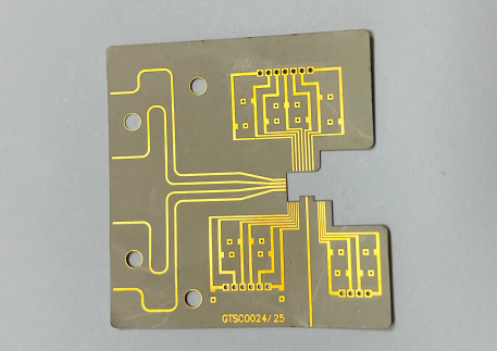
Laser Direct Imaging (LDI) is a highly precise technology used to create intricate circuit patterns on RF PCBs. Unlike traditional photolithography, which uses masks to project circuit designs, LDI uses a focused laser beam to directly write the pattern onto the PCB surface. This method eliminates the need for masks, allowing for greater flexibility and precision in the design process.
How Does LDI Achieve High-Resolution Imaging?
LDI technology achieves high-resolution imaging by using finely focused laser beams with extremely small spot sizes. These lasers can create micro-sized traces with high precision, which is essential for RF PCBs that require intricate, tightly packed signal pathways. LDI's high resolution ensures that even the smallest details in circuit patterns can be accurately reproduced, crucial for high-frequency applications.
The precision required for LDI ensures that even the most complex micro-level signal paths are handled with accuracy. For example, in high-frequency RF designs, where signal integrity is paramount, LDI helps prevent issues like signal loss and interference by maintaining tight control over trace dimensions.
How Does LDI Ensure Precise Circuit Control?
LDI ensures precise control of the circuit layout by using a digital process, where patterns are directly written with a laser, allowing for fine adjustments without the limitations of traditional photomasks. This control enables better line stability and signal integrity, ensuring that the circuit's performance remains consistent even at high frequencies. As a result, LDI is particularly useful in 5G and high-speed communication systems where signal precision is critical.
Micro-Etching Technology and Surface Treatments
How Does Micro-Etching Affect PCB Performance?
Micro-etching is a key process that ensures the surface roughness of copper traces on RF PCBs is controlled precisely. By using chemical or electrochemical methods, micro-etching fine-tunes the surface texture of the copper, optimizing the adhesion of materials and reducing the overall signal loss. The control of copper roughness is especially important in high-frequency applications because it directly impacts signal attenuation and transmission speed.
By achieving a smoother surface, micro-etching helps in reducing the unwanted resistance and parasitic effects that can cause signal degradation. This results in more efficient signal transmission and enhances the overall performance of the RF circuit.
Impact on Impedance Stability and Transmission Efficiency
Micro-etching also plays a critical role in maintaining the impedance stability of the PCB. Impedance mismatches in high-frequency circuits can cause signal reflections, leading to loss of data and performance. By controlling the surface quality of the copper traces, micro-etching ensures that the impedance remains consistent across the entire PCB. This is crucial for applications like 5G or radar systems, where maintaining signal quality is vital for functionality.
ENIG Surface Treatment Advantages
What is ENIG (Electroless Nickel Immersion Gold)?
ENIG is a surface treatment process used to enhance the surface of PCB traces. It involves a two-step process: first, a layer of nickel is electroplated onto the copper surface, followed by immersion in gold to form a thin, durable gold layer. This creates a highly conductive and corrosion-resistant surface that is perfect for high-frequency applications like RF PCBs.
How Does ENIG Improve RF Connector and Soldering Reliability?
ENIG treatment significantly improves the solderability and reliability of RF connectors and joints. The gold layer provides excellent corrosion resistance, reducing the likelihood of oxidation over time, which can compromise the solder joints and connector integrity. This is particularly beneficial in RF communication systems, where reliable connections are essential for signal quality.
For example, in 5G networks, where frequent data transmission requires stable and reliable connections, ENIG treatment ensures that the PCB's connection points remain stable and efficient even under high-frequency conditions.
ENIG's Effect on Corrosion Resistance and Contact Resistance
One of the primary benefits of ENIG is its ability to protect against corrosion, which is a common issue in PCBs exposed to moisture or harsh environmental conditions. The nickel-gold coating provides a robust protective barrier that helps extend the lifespan of the PCB. Additionally, the gold layer reduces contact resistance, ensuring more efficient signal transmission and maintaining high-frequency performance.
The combination of corrosion resistance and low contact resistance makes ENIG an ideal surface treatment for high-performance RF PCBs, particularly in applications like satellite communications and military radar systems, where reliability is critical.
Key Takeaways:
Impedance matching ensures that signals travel efficiently through the PCB without loss or reflection, essential for high-frequency RF circuits.
CO₂ laser drilling enables the creation of micro-sized holes, which reduce parasitic capacitance and inductance, improving signal quality and performance.
Optimizing hole placement and size further enhances electrical performance, ensuring that signal paths remain efficient and free from interference.
These technologies work together to ensure the reliability and high performance of RF PCBs, making them ideal for critical applications such as 5G, satellite communications, and military radar systems.
Ensuring Electrical Performance and Reliability of RF PCBs
The Role of Impedance Matching in RF Circuit Boards
What is Impedance Matching and Why is it Important?
Impedance matching refers to the process of ensuring that the impedance of the RF PCB traces, components, and connectors are consistent throughout the circuit. Impedance is the resistance a signal encounters when passing through a transmission line, such as a PCB trace. If the impedance is mismatched, it can lead to signal reflections, signal loss, and reduced performance. In high-frequency applications, even small mismatches can cause significant issues, including data corruption and communication failures.
For example, in 5G systems, where high-frequency signals are transmitted over short distances, impedance matching is crucial to ensure signal integrity and prevent signal degradation.
How Does Impedance Matching Ensure Signal Integrity and Reduce Signal Reflection?
Impedance matching minimizes signal reflections by ensuring that the RF signal experiences no abrupt changes in impedance along its path. When impedance is mismatched, part of the signal is reflected back to the source, which can interfere with the signal and cause issues such as reduced signal strength or even complete signal loss. By maintaining a consistent impedance, RF signals can travel more efficiently, preserving signal integrity and quality.
In practical terms, this means the source impedance, load impedance, and transmission line impedance must be carefully matched. This is especially important in high-frequency RF circuits, where even slight impedance mismatches can drastically affect signal quality.
How is Impedance Matching Achieved in RF PCB Manufacturing?
Impedance control in PCB design typically involves adjusting the width of the copper traces and the distance between the traces and the PCB's reference ground. Advanced manufacturing techniques, such as Laser Direct Imaging (LDI) and micro-etching, play a significant role in achieving precise impedance control.
LDI enables accurate creation of narrow, consistent trace widths, ensuring that the impedance remains uniform.
Micro-etching is used to control the surface roughness of copper traces, which can also affect impedance.
Both of these technologies ensure that the trace geometry is tightly controlled, reducing variations that can lead to impedance mismatches and maintaining the reliability of high-frequency signals.
Micro-Hole Manufacturing and Electrical Performance
Advantages of CO₂ Laser Drilling for RF Circuit Boards
CO₂ laser drilling is a key technology for creating extremely small and precise holes in RF PCBs. This method uses a high-powered laser beam to vaporize the material, allowing for the creation of micro-sized holes with high precision. These tiny holes are essential for vias, which connect different layers of the PCB and are often critical in high-density designs.
In RF PCBs, minimizing parasitic capacitance and inductance is crucial. CO₂ laser drilling helps achieve smaller hole sizes, which results in reduced parasitic effects. By reducing these unwanted effects, the electrical performance of the PCB improves, particularly for high-frequency signals that are highly sensitive to any form of interference.
How Does Laser Drilling Reduce Signal Interference and Maintain Small Hole Diameters?
The precision of CO₂ laser drilling allows for the creation of micro-holes with minimal thermal impact, reducing the risk of thermal damage to the surrounding copper traces. The small diameter of these holes ensures that signal interference is minimized, as the drill holes are tight and precise, leading to more accurate connections between layers.
In practical terms, smaller vias reduce the surface area of the hole, leading to lower parasitic inductance and capacitance. This helps maintain the signal’s integrity, especially in high-speed, high-frequency applications like 5G or satellite communication systems.
Optimizing Hole Design to Improve Electrical Performance
The design of the holes—specifically, their placement and size—can significantly impact the electrical performance of an RF PCB. Proper hole placement ensures that signal paths are short and direct, reducing the chance of signal degradation or reflection. Additionally, the use of micro-vias—tiny, precise holes used for interconnecting layers—can improve the performance of high-frequency circuits by maintaining cleaner, more efficient signal paths.
For example, in 5G devices, where performance demands are high and signal quality is critical, optimized hole design ensures that RF signals travel with minimal loss and interference, enhancing the overall efficiency and reliability of the system.
Key Takeaways:
Impedance matching ensures that signals travel efficiently through the PCB without loss or reflection, essential for high-frequency RF circuits.
CO₂ laser drilling enables the creation of micro-sized holes, which reduce parasitic capacitance and inductance, improving signal quality and performance.
Optimizing hole placement and size further enhances electrical performance, ensuring that signal paths remain efficient and free from interference.
These technologies work together to ensure the reliability and high performance of RF PCBs, making them ideal for critical applications such as 5G, satellite communications, and military radar systems.
Interlayer Bonding and Manufacturing Processes in RF PCBs
How Vacuum Lamination Technology Optimizes Layer Bonding
Principle and Advantages of Vacuum Lamination Process
Vacuum lamination is a critical process in RF PCB manufacturing, where layers of material are bonded under controlled temperature and pressure in a vacuum environment. The process uses a high-pressure vacuum chamber to eliminate any air trapped between the layers, ensuring uniform adhesion. This ensures that each layer of the PCB is precisely bonded without defects, such as air pockets or voids, which can compromise the integrity of the PCB, especially in high-frequency applications.
The vacuum environment prevents contamination and ensures that no air or moisture remains between the layers, improving the overall durability and performance of the RF PCB. The precise control of the lamination process leads to high-quality bonding, critical for the stable performance of RF circuits, particularly in demanding environments like 5G or satellite communication systems.
How to Avoid Interlayer Voids and Poor Bonding?
To avoid defects like interlayer voids and poor bonding, the temperature and pressure during the lamination process must be carefully controlled. Heat and pressure are applied in a manner that allows each layer to bond evenly without overstressing the material or causing warping. This ensures consistent interlayer bonding across the entire PCB, which is essential for maintaining the mechanical strength and electrical performance of the RF circuit.
In RF PCB manufacturing, achieving a void-free bond is crucial to maintaining signal integrity. Even minor voids between layers can result in signal loss, increased resistance, and reduced overall performance. By maintaining precise control over the lamination process, manufacturers can ensure that the layers remain tightly bonded, enhancing the reliability of the RF PCB over time.
Material Selection and Lamination Process in RF PCBs
Choosing the Right High-Frequency Materials
Selecting the right materials for RF PCBs is vital for achieving the desired performance, particularly in high-frequency applications. Common materials include PTFE (polytetrafluoroethylene), ceramic-filled composites, and high-frequency laminates like RO4000 or Rogers. Each material has its advantages and disadvantages, depending on the specific needs of the application.
PTFE is widely used for high-frequency circuits due to its low dielectric constant and low loss at high frequencies, making it ideal for applications like 5G, satellite communication, and microwave circuits.
Ceramic materials offer excellent thermal stability and low loss at high frequencies, making them suitable for military and aerospace applications, where performance under extreme conditions is critical.
Rogers laminates are popular for their high thermal conductivity and low signal loss, offering a balance between cost and performance in advanced RF applications.
The choice of material significantly affects the signal integrity, thermal management, and electrical performance of the final PCB.
Material and Lamination Process Compatibility
The compatibility between the chosen material and the lamination process is crucial to ensure optimal performance. For instance, materials like PTFE require a specific lamination process due to their non-adhesive nature, meaning they need to be treated with special bonding agents or higher temperatures to achieve reliable bonding.
In contrast, ceramic and Rogers-based laminates can handle higher temperatures during the lamination process, making them more versatile for high-frequency designs. For these materials, controlling the pressure and temperature during lamination helps ensure that the materials bond effectively without degrading their properties.
When selecting materials for specific applications like 5G or satellite communication, it's essential to consider both the electrical performance requirements and the capabilities of the lamination process. The combination of the right material and the optimal lamination technique ensures that the signal quality and long-term reliability of the RF PCB are maintained.
Key Takeaways:
Vacuum lamination ensures precise layer bonding, preventing air pockets and ensuring long-term reliability in high-frequency RF PCBs.
Temperature and pressure control during lamination prevents defects like interlayer voids, which could compromise signal integrity.
The choice of materials like PTFE, ceramics, and Rogers laminates affects signal integrity and performance, and must be paired with appropriate lamination processes.
Compatibility between materials and lamination methods ensures optimal bonding, especially in high-frequency applications like 5G and satellite communications.
These processes and considerations are key to achieving the desired electrical performance and mechanical strength in high-performance RF PCBs. Understanding the intricacies of material selection and lamination technology allows manufacturers to create reliable, high-quality RF circuit boards that meet the needs of demanding applications.
Quality Control and Reliability Testing of RF PCBs
RF PCB Frequency Response Testing and Verification
How to Perform Frequency Response Testing on RF PCBs?
Frequency response testing is essential for verifying the performance of RF PCBs at different signal frequencies. This test ensures that the PCB can handle the required range of frequencies without signal degradation or loss. The most common methods for conducting frequency response tests involve analyzing key parameters such as S-parameters, return loss (also known as reflection loss), and insertion loss.
Key Testing Parameters:
S-parameters: These are a set of measurements used to describe how an RF circuit responds to different input and output signals. S-parameters provide insights into reflection and transmission characteristics, which are crucial for ensuring signal integrity. The most common S-parameters tested are S11 (reflection at the input) and S21 (transmission from input to output).
Return Loss (Reflection Loss): Return loss measures the amount of signal that is reflected back towards the source due to impedance mismatches. A higher return loss indicates better signal transmission, which is critical for ensuring signal quality in RF circuits.
Insertion Loss: This parameter measures the signal attenuation as it passes through the PCB. Minimizing insertion loss is essential to maintain the signal strength, especially in high-speed applications like 5G or satellite communication.
How to Measure These Parameters:
Network analyzers are typically used for S-parameter measurement and return loss testing. These devices apply a range of test frequencies and measure the response of the PCB.
Vector network analyzers (VNA) are used to analyze S11, S21, and other S-parameters, providing precise information on the PCB’s frequency response across its entire operational bandwidth.
By accurately measuring these parameters, manufacturers can validate whether the RF PCB is suitable for high-frequency applications and whether it meets the performance requirements for systems like 5G networks, satellite communications, or radar systems.
Reliability Testing of RF PCBs
Why is Reliability Testing Important for RF PCBs?
Reliability testing is critical for ensuring that RF PCBs can maintain performance under a variety of extreme environmental conditions. Since RF PCBs are used in high-stakes applications like 5G, military communications, and space technology, they must be able to withstand temperature extremes, humidity, vibration, and shock without failing.
How to Ensure Long-Term Stability of RF PCBs in Extreme Environments?
Several types of reliability tests are conducted to simulate harsh operating conditions and ensure that the RF PCB will maintain stable performance over time. These tests include:
Thermal Cycling: This test involves exposing the RF PCB to extreme temperature variations to simulate the environmental conditions it may encounter during operation. The PCB is subjected to thermal stress from both high and low temperatures, checking for issues like delamination or cracking in the material.
Humidity Testing: High humidity can cause corrosion and degrade the performance of the PCB. Humidity exposure tests ensure that the PCB materials are resistant to moisture and that electrical connections remain stable, even in humid environments.
Vibration and Shock Testing: RF PCBs are often used in applications where vibration and shock are common, such as in military or aerospace environments. These tests assess how well the PCB can endure mechanical stress and maintain signal integrity.
Accelerated Life Testing: This involves subjecting the PCB to high-temperature and high-humidity conditions over a shortened time frame, simulating years of use in a fraction of the time. This test helps manufacturers predict the long-term reliability of the PCB.
By conducting these reliability tests, manufacturers can ensure that the RF PCBs will continue to perform as expected, even after prolonged exposure to harsh environmental conditions. The results also help identify potential weak points in the design or materials, allowing engineers to make adjustments before mass production.
Key Takeaways:
Frequency response testing of RF PCBs focuses on parameters such as S-parameters, return loss, and insertion loss to ensure signal integrity and optimal performance in high-frequency applications.
Reliability testing ensures that RF PCBs can withstand extreme temperature, humidity, vibration, and shock conditions, making them suitable for critical applications in 5G, aerospace, and military systems.
By performing these tests, manufacturers can validate the long-term stability and electrical performance of RF PCBs under real-world conditions.
These testing processes are essential for ensuring that RF PCBs are not only effective but also durable, reliable, and ready for use in the most demanding environments.
Conclusion
In conclusion, high-precision RF PCB manufacturing relies on advanced technologies like Laser Direct Imaging (LDI), micro-etching, and vacuum lamination to ensure the stability, reliability, and long-term performance of high-frequency signals. These methods work in harmony to reduce signal loss, minimize interference, and maintain consistent impedance—critical factors for applications in 5G, satellite communications, and other high-performance electronic systems.
Looking to the future, innovations in automation, AI-driven design, and advanced materials will further elevate RF PCB performance, enabling faster, more efficient, and higher-frequency designs. PCBMASTER is at the cutting edge of these advancements, offering a comprehensive suite of solutions that integrate the latest manufacturing technologies with a commitment to exceptional quality and reliability. As a trusted leader in the RF PCB industry, PCBMASTER provides custom-designed circuit boards tailored to meet the stringent demands of modern communication and electronics systems, ensuring the highest levels of performance, durability, and scalability. With PCBMASTER, you gain not only a product, but a partner in creating next-generation electronic systems.
FAQs
What specific performance improvements does Laser Direct Imaging (LDI) technology bring to RF circuit boards?
Laser Direct Imaging (LDI) technology improves the resolution and stability of circuit board designs by precisely forming the traces. This high-precision capability reduces signal distortion and ensures the accurate routing of high-frequency signals, enhancing the overall performance of RF circuits.
What is ENIG surface treatment, and how does it improve RF PCB performance?
ENIG (Electroless Nickel Immersion Gold) surface treatment enhances contact reliability, solderability, and corrosion resistance. This treatment is particularly beneficial for high-frequency signal transmission, as it ensures stable and long-lasting electrical connections, reducing the risk of signal degradation and improving overall PCB performance.
How does CO₂ laser drilling technology help reduce parasitic capacitance in RF PCBs?
CO₂ laser drilling technology enables precise micro-hole designs, minimizing unnecessary electrical interference and reducing parasitic capacitance. This improves signal quality by ensuring clean, uninterrupted signal paths, which is crucial for maintaining high-frequency performance in RF circuits.
How does impedance matching in RF PCBs affect signal quality?
Impedance matching ensures that signals flow through the PCB without reflections or losses. By maintaining consistent impedance across traces, connectors, and components, it significantly improves signal integrity, reducing signal degradation, especially in high-frequency applications such as 5G and satellite communications.
How can manufacturing defects be avoided during the interlayer bonding process in RF PCBs?
The vacuum lamination process effectively prevents manufacturing defects such as interlayer voids or poor bonding. By precisely controlling temperature and pressure during the lamination process, it ensures uniform and defect-free bonding between layers, thus maintaining the integrity and stability of signal transmission.