


Printed Circuit Board Thickness Standards: Industry Guidelines and Best Practices
Printed circuit board (PCB) thickness plays a crucial role in electronics design and manufacturing. Choosing the right thickness is not just a technical detail—it directly affects the board’s electrical performance, mechanical strength, and production reliability.
In this article, we will explain the concept of PCB thickness standards, explore common industry guidelines, share best practices for selecting the right thickness, and provide practical tips for electronics designers and manufacturers. By understanding PCB thickness, you can make better design decisions and ensure your products work safely and reliably.
What is PCB Thickness Standard
1. Definition of PCB Thickness
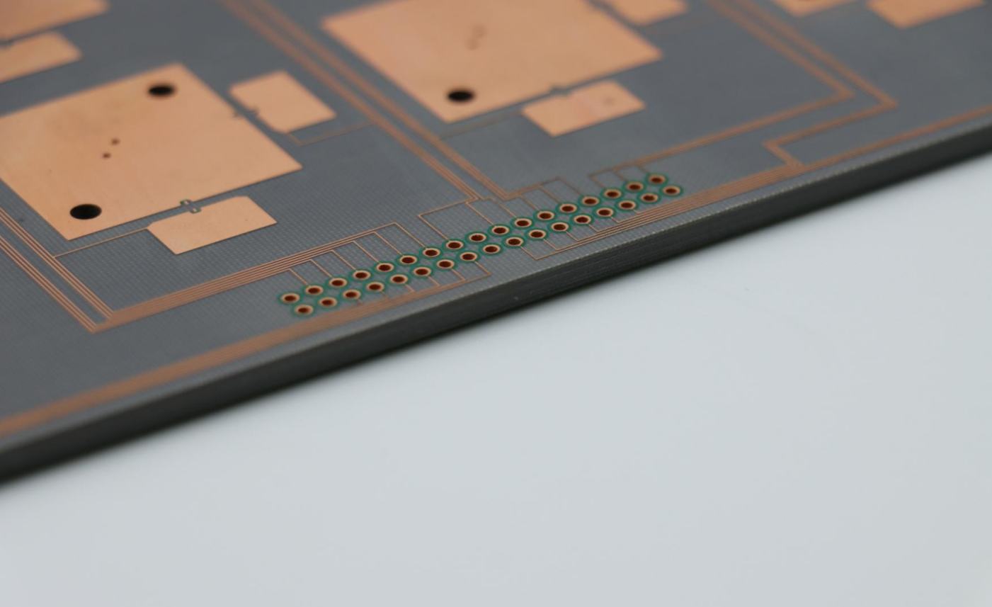
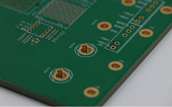
PCB thickness refers to the total distance measured from the top copper surface to the bottom copper surface of the board. This dimension is not just a physical measurement—it plays a crucial role in determining how the PCB performs in both electrical and mechanical aspects. Choosing the correct thickness ensures that the board can handle the intended current, signal integrity requirements, and mechanical stress during operation.
2. Common Thickness Specifications
Common thicknesses are standardized to help designers and manufacturers select the right board easily. Standard sizes include 0.4mm, 0.6mm, 0.8mm, 1.0mm, 1.2mm, 1.6mm (most commonly used), and 2.0mm.
Each thickness has its own application:
l Thinner boards (0.4–0.8mm) are often used in compact electronics where space is limited.
l Thicker boards (1.6–2.0mm) are suitable for supporting heavier components or high-power circuits.
l Specialized PCBs may go beyond these ranges, such as ultra-thin boards under 0.4mm for flexible devices or extra-thick boards over 2.0mm for industrial and high-current applications.
3. Importance of PCB Thickness
The importance of PCB thickness spans several dimensions:
l Electrical Performance: Thickness directly affects impedance, signal integrity, and crosstalk in high-speed circuits. Thicker boards can support higher voltage isolation, while thinner boards may be more suitable for low-voltage, compact designs.
l Mechanical Strength: Thicker PCBs resist bending and warping better, which is crucial for boards with heavy components or in environments with vibration. Thinner PCBs provide flexibility but require careful handling to avoid damage.
l Thermal Management: Board thickness influences heat dissipation. Thicker boards can spread heat more effectively, reducing the risk of component overheating, while thin boards may need additional cooling solutions.
Selecting the right PCB thickness is a balance between electrical requirements, mechanical durability, and thermal efficiency. It ensures the PCB performs reliably throughout its life, whether it’s used in consumer electronics, industrial equipment, or high-frequency communication devices.
Industry Guidelines of PCB Thickness Standard
1. IPC Standards
Following industry guidelines is essential to ensure PCBs are reliable, perform well, and are safe to use. The IPC standards are widely recognized references in the PCB industry. For example:
l IPC-2221 provides general recommendations for PCB design, including layer stacking, trace width, and spacing considerations.
l IPC-6012 focuses on rigid boards, specifying thickness ranges, mechanical strength, and testing procedures.
These standards define acceptable tolerances, inspection methods, and quality requirements, which help prevent common issues such as warping, weak solder joints, or signal integrity problems. Adhering to IPC standards ensures that PCBs produced by different manufacturers remain consistent in quality, which is crucial for commercial products, aerospace, medical devices, and other critical applications.
2. Board Type and Material
The type of PCB and the material used greatly influence the suitable thickness. Designers must consider the number of layers, electrical performance requirements, mechanical strength, and thermal management when selecting thickness.
l Single-layer boards are typically thinner, ranging from 0.4mm to 1.0mm, because they carry fewer components and have simpler routing. They are common in simple electronics like LED boards, small sensors, and toys.
l Double-layer boards usually range from 0.8mm to 1.6mm, providing a balance between mechanical strength and electrical performance. These are widely used in consumer electronics, industrial controllers, and automotive circuits.
l Multi-layer boards often require 1.6mm to 2.0mm or more to accommodate multiple signal and power layers. High-speed computing, communication devices, and advanced electronics frequently use multi-layer boards.
Material choice also affects thickness:
l FR4 is the most common material and typically ranges from 0.4mm to 2.0mm, offering good mechanical strength, electrical insulation, and thermal stability.
l Rogers material is used in high-frequency applications. Its thickness is often thinner or specially customized to maintain signal integrity and controlled impedance.
l Ceramic or metal-core boards may require extra thickness to enhance thermal dissipation, mechanical support, or durability for high-power applications.
3. Manufacturing Tolerances
Even with careful design, the final PCB thickness may slightly differ due to variations in copper layers, lamination, and fabrication processes. For instance, a board with heavy copper traces may be slightly thicker in some areas, while multi-layer lamination can introduce minor deviations.
Manufacturers usually provide tolerance specifications, such as ±0.1mm, to account for these variations. Proper planning of copper weight, layer stacking, and lamination processes ensures that the finished PCB meets electrical, mechanical, and assembly requirements. Ignoring tolerances can lead to problems like poor fit in enclosures, uneven soldering, or signal integrity issues.
4. Special Application Requirements
Certain applications require carefully controlled thicknesses to meet performance standards:
l High-frequency PCBs need precise, often thinner layers to maintain correct impedance and reduce signal loss. Small deviations in thickness can affect transmission lines and cause signal distortion.
l Flexible PCBs require ultra-thin substrates that allow the board to bend without cracking. Thickness selection here balances flexibility with durability.
l Rigid-flex PCBs combine rigid and flexible areas. Designers must carefully manage thickness transitions to maintain reliability while ensuring the flexible parts can bend as intended.
By following these guidelines, designers ensure that the PCB functions correctly, maintains mechanical strength, and meets the intended electrical performance, which is critical for both prototype testing and large-scale production.
Best Practices of PCB Thickness Standard
1. Design Phase Considerations
Choosing the correct PCB thickness starts in the design phase and affects every aspect of the board’s performance. Designers must consider:
l Product Function: For portable or handheld electronics, thinner boards may be necessary to fit compact enclosures. For power electronics or boards with heavy components, thicker boards help prevent bending or mechanical failure.
l Physical Size and Layout: The overall size and component density influence how thick or thin the PCB should be. Large, heavy boards often benefit from added thickness to maintain rigidity.
l Mechanical Structure: Some devices experience vibration, bending, or repeated handling. Designers must choose a thickness that balances flexibility and durability, preventing cracks or fractures during use or assembly.
Proper planning at this stage ensures the board can be manufactured reliably and function safely in its intended environment.
2. Signal Integrity Optimization
PCB thickness has a direct impact on electrical performance, especially in high-speed or high-frequency designs:
l Impedance Control: Trace impedance is influenced by the distance between signal layers and the reference plane. Selecting the correct board thickness ensures consistent impedance, which reduces signal reflection and maintains data integrity.
l Crosstalk Reduction: Adequate thickness and layer spacing help minimize interference between adjacent traces, improving overall signal quality.
l Stable Transmission: For applications like RF communication, high-speed data buses, or digital audio/video circuits, precise thickness selection helps prevent errors and signal degradation over long traces.
Optimizing thickness for signal integrity ensures reliable, high-performance operation in demanding electronic systems.
3. Mechanical Strength and Durability
PCB thickness affects how boards handle physical stress:
l Thin Boards: While flexible, thin boards (<0.8mm) are prone to bending, warping, and cracking during handling, assembly, or vibration. Designers should reinforce critical areas or add mechanical supports where needed.
l Thick Boards: Boards >1.6mm are mechanically stronger but harder to process. They require careful drilling, soldering, and lamination to avoid defects such as delamination, stress cracks, or uneven layers.
l Reinforcement Techniques: Adding support materials, copper planes, or edge stiffeners can help balance flexibility and strength, ensuring durability during the PCB’s lifecycle.
Correctly balancing thickness ensures that boards survive assembly and long-term use without mechanical failure.
4. Manufacturing Process Compatibility
PCB thickness must align with fabrication capabilities to ensure smooth production:
l Drilling and Cutting: Extremely thin boards may tear during drilling or routing, while thick boards may require specialized drill bits and longer processing time.
l Soldering and Lamination: Proper thickness ensures heat is evenly distributed during soldering and lamination, avoiding warping or defects.
l Equipment Limitations: Some automated assembly lines have constraints on board thickness. Designers must verify that their chosen thickness is compatible with the manufacturer’s equipment to prevent delays or additional costs.
Ensuring compatibility avoids production issues and maintains high yield rates during manufacturing.
5. Testing and Verification
After the PCB is fabricated, rigorous testing confirms that thickness and performance meet design specifications:
l Measurement Tools: Micrometers or laser thickness gauges are used to verify total board thickness and individual layer thicknesses.
l Functional Testing: Boards are subjected to electrical tests to ensure proper signal transmission and component performance.
l Reliability Assessments: Mechanical stress tests, bending tests, and thermal cycling simulate real-world conditions, confirming that the board will perform reliably under actual use.
Testing and verification ensure the final PCB meets both mechanical and electrical requirements, avoiding failures in the field.
Tips for Choosing the Right PCB Thickness
1. Think About Your Product Type
Different products have very different requirements for PCB thickness based on size, durability, and functionality:
l Consumer Electronics: Devices like smartphones, tablets, and smartwatches usually require thin boards (around 0.8–1.0 mm). Thin PCBs save space and reduce overall product weight, which is critical for portability. These boards must also handle dense component placement without warping or short circuits.
l Industrial Control Systems: These environments are tough, with vibration, temperature fluctuations, and mechanical stress. Thicker boards (1.6 mm or more) provide extra strength and reliability, helping prevent damage during long-term operation in factories or plants.
l Aerospace Products: Aerospace applications demand high reliability under vibration, extreme temperatures, and mechanical stress. The thickness must be carefully chosen along with special materials (like Rogers or metal-core boards) to ensure the board maintains its electrical and mechanical properties in harsh conditions.
l Medical Devices: Precision and stability are critical. Medical PCBs may need a specific thickness to fit compact enclosures, handle repeated cleaning or sterilization, and ensure accurate, long-term operation. Thickness selection here is tied closely to safety, accuracy, and compliance with regulatory standards.
Understanding the product’s operating environment helps determine the baseline thickness needed for safety, reliability, and usability.
2. Consider Your Design Limits
PCB thickness must fit the physical and functional constraints of your product:
l Limited Space: When the product is compact, thinner boards allow components to fit without increasing device size. This is crucial for wearable devices, compact electronics, or devices with multiple stacked boards.
l Flexibility Requirements: If the board must bend or fold, such as in flexible displays, foldable phones, or wearable sensors, choose very thin or flexible substrates. This prevents cracking and maintains functionality during repeated bending.
l Power and Heat Management: Boards carrying high currents or generating heat need extra thickness and sufficient copper layers for better thermal dissipation. Thick PCBs prevent overheating, support heavier components, and maintain structural integrity under high power loads.
Evaluating these design limits ensures your board meets both physical and electrical requirements without risking performance issues.
3. Match Your Manufacturer’s Capabilities
Not all PCB manufacturers can produce every thickness or material type:
l Standard Thickness Support: Most factories handle common thicknesses like 1.0 mm or 1.6 mm. If your design falls within these ranges, manufacturing is straightforward.
l Special Thicknesses: Ultra-thin (<0.4 mm) or extra-thick (>2.0 mm) boards may require specialized equipment and handling. Confirm that the manufacturer can maintain tight tolerances, proper lamination, and drilling quality.
l Tolerance and Quality: Even small deviations in thickness can affect impedance, mechanical strength, or assembly fit. Choose a supplier who guarantees precise control over thickness and layer alignment.
Matching the board thickness with manufacturing capabilities avoids production delays, reduces defects, and ensures that your PCB functions as intended.
4. Think About the Cost
PCB thickness directly impacts manufacturing cost, so budget planning is important:
l Thin Boards: Extremely thin boards may need extra care during lamination, drilling, and handling to prevent warping or breakage. This can increase labor or processing costs.
l Thick Boards: Boards thicker than 2 mm require longer drilling and cutting times and may need stronger lamination presses or specialized tooling. These factors increase production costs.
l Balance Performance and Budget: Evaluate whether the added cost of very thin or very thick boards is justified by performance needs. Avoid over-engineering—use thicker or thinner boards only when necessary for mechanical, electrical, or thermal reasons.
Careful planning ensures you get the right board for your application without overspending on unnecessary material or processes.
Conclusion
Choosing the right PCB thickness is more than just a number—it directly affects your product’s performance, reliability, and durability. Selecting a proper thickness ensures that your board can handle electrical requirements, mechanical stress, and heat management, while fitting perfectly into your product design.
By following industry standards like IPC-2221 and IPC-6012, and applying best practices—such as considering product type, signal integrity, mechanical strength, and manufacturing capabilities—you can make informed decisions that reduce errors and improve product quality.
Take action today: carefully evaluate your PCB requirements, consult the guidelines, and work with experienced PCB manufacturers like PCBMASTER to select the ideal board thickness for your project. This ensures your designs are not only functional but also reliable and production-ready.
FAQs
1. Can PCB thickness affect heat management in electronic devices?
Yes, PCB thickness plays an important role in handling heat. Thicker boards with good copper layers can spread heat better, which prevents components from overheating. Thin boards may heat up faster, especially if they carry high current. For devices like power supplies or LED boards, using a thicker PCB helps maintain safe temperatures and prolongs the life of the electronics.
2. How does PCB thickness influence bending or flexibility?
The thickness of a PCB determines how much it can bend. Thin boards or flexible PCBs can bend without breaking, which is important for wearable devices or foldable electronics. Thicker boards are stronger and more rigid, but they can crack if forced to bend. Choosing the right thickness ensures that the board matches the product’s mechanical needs.
3. Can choosing the wrong PCB thickness affect signal performance?
Yes, thickness affects electrical performance, especially for high-speed or high-frequency circuits. If the board is too thin or too thick for the signal design, it can change the impedance, cause signal reflection, or create crosstalk between traces. Careful selection of PCB thickness ensures stable signal transmission and reduces errors in sensitive electronics like communication devices or computer boards.

