


How Printed Circuit Board Layers Impact PCB Design and Performance
Behind every well-functioning electronic device lies a carefully engineered printed circuit board (PCB), where the arrangement of layers plays a pivotal role in performance. From the subtle intricacies of signal transmission to the challenge of managing heat, these layers are more than just structural—they’re the foundation of efficient, reliable operation. Yet, the true impact of PCB layers often remains hidden until performance issues arise. The way these layers interact with each other can make or break a design, influencing everything from signal integrity to electromagnetic interference (EMI). As the demands on modern electronics continue to grow, understanding the role of each layer is key to pushing your designs to the next level. Let's explore how these layers shape the performance of every circuit, one connection at a time.
Introduction to Printed Circuit Board (PCB) Layers
What Are PCB Layers?
A printed circuit board (PCB) is much more than a flat piece of material; it’s a multi-layered system designed to connect and support electronic components. The layers of a PCB are crucial for directing electrical signals, providing grounding, and ensuring the board’s overall functionality. At its core, a PCB consists of several different layers, each with a specific role that contributes to the board’s performance.
Signal Layers
These layers are responsible for carrying electrical signals between the components on the PCB. In a basic design, signal layers might be limited to one or two, but in more complex circuits, multiple signal layers are used to separate different types of signals and ensure efficient operation. For example, a high-speed circuit like a microprocessor board may require several signal layers to handle the dense routing of data signals.
Power and Ground Planes
Power and ground layers are typically used to provide consistent electrical power across the board and ensure a solid reference ground for all signals. The ground plane helps to reduce noise and provides a path for current to return, improving overall signal integrity. Power planes distribute power efficiently to different parts of the PCB, making sure each component receives the right voltage. These layers are particularly crucial in designs where high-speed or high-power components are involved, as they help minimize interference and maintain stable operation.
Substrate
The substrate is the base material that forms the foundation of the PCB. It’s typically made from materials like FR4 (a composite of glass and resin) or, in high-performance designs, materials like Teflon or ceramics. The substrate provides mechanical support, insulation, and some thermal management to the board. The material choice for the substrate impacts the PCB’s overall strength, flexibility, and thermal conductivity.
Example
A simple PCB might be a single-layer board that combines a signal layer and a ground layer, often used in basic electronics like resistors or capacitors. In contrast, a multi-layer PCB, often found in smartphones or computers, might have many signal layers interspersed with power and ground planes, each layer contributing to a more complex and higher-performance design.
The Role of Layers in PCB Construction
The structure of a PCB is carefully designed to balance functionality and performance, with each layer serving a distinct purpose. The layered arrangement enables efficient signal transmission, grounding, and heat dissipation, ensuring that electronic components work together seamlessly.
Layered Structure in PCB Fabrication
PCB fabrication starts with the creation of the substrate, which serves as the base for the entire assembly. As the design progresses, additional layers of copper are added to form the electrical connections. These layers are then etched to create the conductive paths that will carry the electrical signals. Depending on the complexity of the design, more layers can be added to separate different functions like power delivery, ground planes, and signal paths. The entire process culminates in the final multi-layered PCB, ready for use in various applications.
Importance of Each Layer for Functionality and Performance
Each layer within a PCB contributes to the overall functionality of the device. Signal layers are critical for routing communication between components, while power and ground planes ensure that electrical energy is distributed efficiently and that signals remain clean and free of noise. The substrate layer, though often overlooked, provides mechanical stability and thermal dissipation, helping to prevent overheating and ensuring that the components remain securely in place.
Signal Layers: Essential for routing high-frequency signals with minimal interference.
Power and Ground Planes: Critical for noise reduction, stable power delivery, and signal reference grounding.
Substrate: Provides mechanical and thermal stability to prevent warping or damage during use.
Step-by-Step Process: From Single-Layer to Multi-Layer PCBs
Single-Layer PCB: The simplest form of PCB, typically used in low-density applications where minimal components are involved. It consists of one conductive layer (usually copper) and one insulating substrate.
Double-Layer PCB: This type includes two conductive layers, one on each side of the substrate, and is used when additional connections are needed.
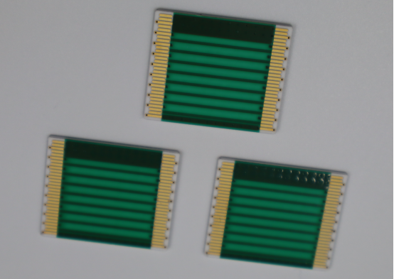
Multi-Layer PCB: Complex designs use multiple layers of conductive material, stacked and interconnected through vias (small drilled holes). Multi-layer PCBs are essential for high-density, high-performance circuits, like those in mobile phones or computers.
The number of layers a PCB has directly affects its complexity, performance, and manufacturing cost. While a single-layer PCB may be suitable for simpler devices, multi-layer PCBs are essential for more complex systems, offering increased capacity for routing, better signal integrity, and reduced electromagnetic interference (EMI).
Types of PCB Layers and Their Functions
Signal Layers
Definition and Purpose
Signal layers are the conductive pathways within a PCB that carry electrical signals between the various components, such as resistors, capacitors, and integrated circuits. These layers are the core element for routing high-frequency signals across the board, ensuring that electrical currents flow efficiently between different parts of the system. Signal layers are often made from copper, etched into precise paths, known as traces, which are then connected to various pads and vias.
Example
In high-frequency circuits, such as those used in telecommunications or Wi-Fi devices, signal layers play a critical role. For example, in a Wi-Fi router, high-frequency signals are routed through multiple signal layers to maintain a clean and uninterrupted data stream. A typical high-frequency PCB may have several signal layers separated by ground or power planes to reduce noise and improve signal integrity.
Impact on Performance
The quality of signal transmission is largely dependent on the design of the signal layers. Proper impedance control and trace width are crucial for maintaining high-frequency signal integrity. For instance, if a signal trace is too narrow or too long, it may lead to signal degradation or reflections, negatively affecting performance. Well-designed signal layers with appropriate trace widths and controlled impedances help reduce these issues, ensuring that signals travel efficiently without interference or loss.
Power and Ground Layers
Purpose
Power and ground layers are dedicated planes within the PCB that provide stable power distribution and a common reference point for all components. The power plane distributes electrical energy from the power source to different sections of the board, while the ground plane serves as the return path for the current. These layers also play a key role in reducing noise and ensuring clean, stable signal operation.
Example
Power and ground planes are essential in high-power applications, such as in power supply units (PSUs) or graphics processing units (GPUs). For example, in a GPU, the power plane ensures that each section of the graphics card receives the correct voltage, while the ground plane minimizes interference between high-speed data signals and the power delivery system.
Effects on Performance
The inclusion of power and ground planes significantly improves PCB performance by:
Reducing Noise: These layers provide a solid reference ground, which helps reduce electromagnetic interference (EMI) and minimizes cross-talk between adjacent signals.
Improving Signal Quality: By maintaining a consistent ground reference, the signal layers experience less fluctuation, leading to cleaner signal transmission.
Better Thermal Management: Power planes help distribute heat more evenly across the board, reducing the likelihood of hot spots that could affect component longevity or performance.
Substrate Layer
Description
The substrate layer is the base material of the PCB, providing mechanical support for all other layers. Typically made from fiberglass-reinforced epoxy resin (FR4), the substrate offers electrical insulation between the conductive copper layers. The choice of substrate material is crucial because it determines the PCB’s strength, flexibility, and thermal characteristics.
Functions
Mechanical Support: The substrate layer provides the structural foundation for the PCB, holding all components and other layers in place.
Insulation: The substrate ensures that the conductive copper traces do not short-circuit each other, providing electrical isolation between layers.
Thermal Conductivity: The substrate also helps in heat dissipation, though its performance depends on the material chosen. For example, materials like Teflon or ceramic substrates are better suited for high-temperature applications.
Example
FR4 is the most common substrate material used in consumer electronics due to its cost-effectiveness and balance between performance and durability. However, for high-frequency applications like radio frequency (RF) circuits, materials like Rogers or Teflon are preferred due to their superior thermal conductivity and lower signal loss. These materials, while more expensive, ensure better performance in specialized applications.
Cost vs. Performance
While FR4 is economical, it’s not ideal for high-speed or high-power applications due to its limitations in thermal conductivity and signal integrity. High-performance materials like Rogers provide superior dielectric properties but come at a higher cost. The choice of substrate depends on the performance requirements of the final product.
Via and Layer Interconnects
Role of Vias in Connecting Multiple Layers
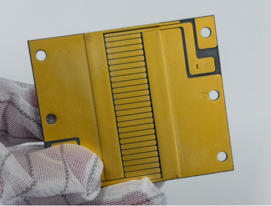
Vias are small holes drilled through the PCB that allow electrical connections between different layers. By placing vias at specific points, designers can interconnect signal layers, power planes, and ground planes to form a complete electrical circuit. Vias are an essential part of multi-layer PCB designs, where multiple signal and power layers need to be interconnected to ensure the proper flow of signals and power.
Types of Vias
There are several types of vias used in PCB design, each with its specific purpose:
Through-Hole Vias: These run from the top layer to the bottom layer of the PCB. Through-hole vias are common in traditional designs, where the via is visible on both sides of the board.
Blind Vias: These only connect an outer layer to one or more inner layers. Blind vias are often used in high-density designs, where routing on the outer layers is limited.
Buried Vias: These connect only inner layers and are not visible on the outer layers of the PCB. Buried vias are typically used in more complex, high-performance designs where minimizing space is crucial.
Example
In a multi-layer PCB, the placement of blind or buried vias can significantly impact signal integrity. For instance, in a high-speed digital board, poorly placed vias can cause signal reflection, creating interference or slowing down data transmission. On the other hand, well-planned vias ensure that signal paths remain uninterrupted, minimizing any loss or delay.
Impact on Signal Integrity and Manufacturing Cost
Via design affects both the performance and the cost of a PCB. In high-speed circuits, using vias can sometimes result in signal distortion or impedance mismatch. The number of vias, their size, and their placement can influence both the electrical performance of the PCB and its manufacturing cost. Minimizing via count by optimizing layer stack-up and using advanced via designs, such as microvias, can reduce manufacturing complexity and cost while improving signal integrity.
Impact of PCB Layer Count on Design and Performance
Single-Layer vs. Multi-Layer PCBs
Definition
Single-layer and multi-layer PCBs differ primarily in their construction and complexity. A single-layer PCB consists of just one conductive layer, typically on one side of a non-conductive substrate, while a multi-layer PCB consists of several layers of conductive material separated by insulating layers. These multiple layers are interconnected via vias, allowing for more complex routing of electrical signals. Multi-layer PCBs enable higher density and more sophisticated designs compared to single-layer boards.
Example
Single-Layer PCB: A simple PCB might be used in basic consumer products like calculators or simple household gadgets. These devices have low-density circuits, making a single-layer PCB sufficient to route the necessary signals.
Multi-Layer PCB: In contrast, complex products like smartphones, laptops, and medical devices require multi-layer PCBs. For instance, smartphones utilize multi-layer PCBs to fit the complex routing of power, ground, and signal lines into a small, compact space. The layers help manage high-frequency signals, reduce interference, and make room for advanced functionalities.
Trade-offs
While multi-layer PCBs offer enhanced performance, there are several trade-offs:
Cost: Multi-layer PCBs are more expensive to manufacture due to the added complexity, materials, and processing steps.
Manufacturing Complexity: Creating multi-layer PCBs requires precise alignment and bonding of layers, making the process more complicated and prone to defects.
Performance: Multi-layer PCBs can improve performance by reducing noise and increasing the routing capacity, but this comes at the cost of potential signal integrity issues if the design is not carefully managed.
When to Use Multi-Layer PCBs
Key Considerations
Space Constraints: Multi-layer PCBs are ideal when the available space is limited. As electronic devices become smaller and more compact, multi-layer designs help pack more functionality into a smaller form factor.
High-Frequency Requirements: High-frequency circuits, such as those used in communication devices, require multi-layer PCBs to maintain signal integrity. The additional layers help reduce the distance signals must travel, minimizing signal degradation.
Design Complexity: Complex systems with a large number of components and connections benefit from the use of multi-layer PCBs, as they allow for better routing and organization of signals.
Example
Consumer Electronics: Devices like smartphones, tablets, and smartwatches need multi-layer PCBs to handle the high-density circuits, power management, and data transmission required in such small packages.
Medical Devices: Advanced medical equipment like MRI machines or implantable devices rely on multi-layer PCBs to integrate various functionalities and ensure high reliability, especially for critical applications where performance and safety are paramount.
Automotive Systems: Multi-layer PCBs are also widely used in automotive electronics, including advanced driver-assistance systems (ADAS), where space and reliability are essential in ensuring safe and effective operation.
Challenges with Multi-Layer PCBs
Manufacturing Complexities
The manufacturing process for multi-layer PCBs involves several steps, each requiring precision:
Layer Stacking: Aligning and stacking multiple layers of copper and insulating materials requires meticulous planning and accuracy to ensure electrical continuity.
Alignment: Ensuring that all layers are properly aligned during the lamination process is crucial, as any misalignment can result in faulty connections or reduced performance.
Layer Bonding: The process of bonding the layers together can introduce defects if not performed correctly, leading to weak connections or delamination over time.
Potential Performance Issues
While multi-layer PCBs offer superior functionality, they also introduce some performance challenges:
Signal Interference: As the number of layers increases, the risk of signal interference, especially between closely packed signal lines, also increases. Cross-talk between adjacent signal layers can lead to degraded signal quality.
Crosstalk: In multi-layer designs, signal traces that run in close proximity can cause unwanted coupling of signals, leading to noise or erroneous data.
Layer Separation: In extreme cases, improper bonding or thermal stress can cause layer separation, which can lead to circuit failure or degradation over time.
Solution Strategies
Controlled Impedance: To mitigate signal integrity issues, PCB designers can use controlled impedance techniques. By carefully controlling trace width, spacing, and layer stack-up, designers can ensure that signals pass through the PCB with minimal interference and loss.
Proper Design Rules: Following best practices in PCB design—such as minimizing trace length, using proper grounding techniques, and separating sensitive signals—can significantly reduce the risk of performance issues.
Via Design Optimization: Using optimized via designs (e.g., microvias) can help minimize the impact of signal degradation by reducing the number of vias and their associated parasitic effects.
How PCB Layer Design Affects Signal Integrity and EMI
Signal Integrity Challenges
Importance of Controlled Impedance and Minimized Crosstalk
Signal integrity is essential for ensuring that electrical signals travel cleanly and accurately between components on a PCB. A key factor in maintaining signal integrity is controlled impedance, which refers to managing the resistance a signal encounters as it travels through the PCB. If the impedance is not controlled, the signal can experience reflections, distortions, or loss of data, leading to poor performance or failure. Additionally, crosstalk, which occurs when signals from adjacent traces interfere with each other, can cause noise and signal degradation, especially at high frequencies.
Example: How Trace Width and Spacing Affect Signal Transmission Quality
The width and spacing of traces on a PCB are directly related to the impedance of the signal path. If traces are too narrow or too close together, the impedance may become inconsistent, leading to signal reflections or noise. For example, in high-speed digital circuits, narrow traces may cause higher resistance, which results in slower signal propagation and potential data errors. By carefully adjusting trace width and spacing, designers can ensure the signal travels at the right speed without distortion or delay.
Design Techniques to Improve Signal Integrity
Differential Pairs: This technique involves routing two traces close together, carrying opposite signals. By doing so, the signals cancel out any noise picked up along the way, improving overall signal quality. Differential pairs are widely used in high-speed designs such as USB, Ethernet, and HDMI.
Controlled Trace Width: Ensuring that trace width is consistent across the board helps maintain stable impedance, crucial for high-speed signals. Designers calculate the trace width based on factors like PCB material, layer stack-up, and the desired impedance.
Proper Layer Stack-Up: The arrangement of signal layers in relation to ground and power planes can significantly impact signal integrity. By placing signal layers closer to ground planes, designers can minimize the effect of noise and interference, ensuring cleaner signal transmission.
Managing Electromagnetic Interference (EMI)
How Multiple Layers Contribute to EMI Reduction
Multi-layer PCBs are highly effective at reducing electromagnetic interference (EMI), which can disrupt signal transmission. The multiple layers in a PCB act as shields, helping to contain EMI within specific regions of the board. Ground planes, placed adjacent to signal layers, absorb and reroute unwanted electromagnetic waves, preventing them from radiating outward and interfering with neighboring components or external devices. This is especially important in high-frequency applications, where EMI can significantly degrade performance.
Example: Shielding and Grounding Techniques Used to Reduce EMI in High-Frequency Designs
In high-frequency designs, shielding and grounding are key to minimizing EMI. A common method involves surrounding sensitive signal traces with a ground plane, effectively creating a Faraday cage that blocks external electromagnetic fields. Shielded traces and vias can also be used to divert EMI away from critical components. For instance, in RF (radio frequency) designs used for telecommunications, a well-placed ground plane and shielding can prevent interference from external radio signals, ensuring clear and reliable data transmission.
Comparison: Effectiveness of Ground Planes vs. Power Planes in Minimizing EMI
Ground Planes: Ground planes are highly effective at minimizing EMI because they provide a direct return path for current, which reduces the risk of creating a loop that could emit electromagnetic waves. By placing signal layers close to a ground plane, designers can shield sensitive signals from noise, especially in high-frequency designs.
Power Planes: While power planes help deliver stable power across the PCB, they are less effective at minimizing EMI compared to ground planes. However, power planes can still reduce EMI when paired with ground planes, as they help maintain a stable reference voltage and prevent fluctuations that might induce noise.
High-Frequency Design Considerations
The Importance of PCB Layers in High-Speed Digital and RF Applications
In high-speed digital circuits and radio frequency (RF) applications, PCB layer design plays a pivotal role in maintaining signal quality and overall performance. For high-frequency designs, signal traces need to be carefully routed and controlled to prevent reflections, loss, or distortion. The layer stack-up, trace width, and the distance between signal layers are critical factors that influence signal transmission at high frequencies.
Example: Design Tips for RF PCBs Used in Telecommunications and Radar Systems
In RF PCB designs, such as those used in telecommunications or radar systems, the goal is to ensure that signals travel with minimal loss and distortion. Techniques like controlled impedance (e.g., microstrip or stripline) are essential to ensure that signals are transmitted at the correct speed and with the right voltage levels. Designers often use co-planar waveguides to control the propagation of high-frequency signals, and special care is taken to route RF traces away from other high-speed digital signals to avoid interference.
Impact on Performance: How Incorrect Layer Stacking Can Lead to Signal Degradation
Improper layer stacking in high-frequency designs can lead to significant performance issues. If the signal layer is placed too far from the ground or power plane, the signal can become noisy or unstable, especially at higher frequencies. Similarly, improper placement of power and ground planes can introduce impedance mismatches or cause excessive noise. These issues can result in degraded signal quality, loss of data, or even complete system failure. Correct layer stacking, with a signal layer close to a ground plane, helps maintain clean and reliable signal transmission, ensuring optimal performance in high-speed or high-frequency applications.
Thermal Management in PCB Layer Design
Heat Dissipation in Multi-Layer PCBs
Role of Power and Ground Planes in Heat Distribution
In multi-layer PCBs, power and ground planes play a critical role in thermal management. These planes not only help with stable power distribution and grounding but also act as heat sinks, spreading heat more evenly across the board. By providing a larger surface area for heat dissipation, the power and ground planes help to lower the overall temperature of the PCB, preventing hotspots that could damage sensitive components. The conductive copper material in these planes allows for efficient heat transfer, which is essential in high-performance designs where heat generation is a significant concern.
Example: Thermal Management in High-Power Devices like CPUs and GPUs
High-power devices like CPUs and GPUs generate significant heat during operation. In these applications, effective thermal management is crucial to prevent overheating, which can lead to throttling or failure. Multi-layer PCBs often incorporate power and ground planes strategically placed to ensure the heat from these high-power components is spread evenly and quickly dissipated. For example, in a graphics card, the power plane can help absorb and distribute the heat generated by the GPU, while the ground plane provides a stable reference and assists with heat transfer.
Techniques for Effective Thermal Management
Several techniques can be employed to manage heat in multi-layer PCBs:
Heat Sinks: These are attached to heat-sensitive components to absorb and dissipate heat away from the device. They are particularly common in high-power applications such as CPUs, power supplies, and LEDs.
Via Stitching: Via stitching involves adding small vias (holes) between layers to enhance thermal conduction. These vias help distribute heat more effectively from high-temperature areas to lower-temperature regions of the PCB, preventing localized overheating.
Copper Planes: Using copper planes, especially in high-power applications, helps enhance thermal conductivity. Copper’s excellent thermal properties make it an ideal material for transferring heat away from sensitive components.
The Impact of Layer Count on Thermal Performance
How Multiple Layers Influence the Ability to Dissipate Heat
The number of layers in a PCB can significantly affect its ability to manage heat. While single-layer PCBs are limited in their capacity to distribute heat, multi-layer PCBs allow for more sophisticated thermal management. The additional layers provide more pathways for heat to spread, as power and ground planes can be strategically placed to absorb and dissipate heat across the board. In multi-layer designs, the heat generated by high-power components can be spread across multiple layers, reducing the chance of localized overheating and improving overall thermal stability.
Example: Comparing Single-Layer PCB with Multi-Layer PCB in Terms of Heat Conduction
A single-layer PCB typically relies on the thin copper traces on the surface to conduct heat. However, its limited surface area and lack of internal planes can make heat dissipation inefficient, particularly in high-power applications. In contrast, a multi-layer PCB offers more internal copper layers, which can be used as power and ground planes for heat conduction. For example, in a power supply unit (PSU), a multi-layer PCB can have dedicated ground and power planes that not only route signals but also spread heat more evenly. The additional layers increase the board’s ability to absorb heat from high-power components and distribute it away from critical areas.
Design Considerations: Thermal Vias, Material Choice, and Layer Structure for Better Heat Management
When designing a multi-layer PCB for optimal thermal performance, there are several key factors to consider:
Thermal Vias: These are specialized vias designed specifically for heat transfer. Thermal vias are placed near high-heat-generating components and help channel heat from the surface to the inner layers or to the board's edge, where it can be dissipated more effectively.
Material Choice: The material used for the PCB substrate also plays a significant role in heat management. Materials like ceramic and Teflon offer better thermal conductivity than traditional FR4 and are often used in high-performance applications that require superior heat dissipation. The thermal conductivity of the substrate material directly influences how quickly heat is transferred away from hot spots.
Layer Structure: The arrangement of the layers in the PCB should be optimized for thermal management. Placing power and ground planes adjacent to signal layers allows heat to be efficiently absorbed and conducted away from sensitive components. Additionally, designers may choose to incorporate multiple thermal vias and copper pours to further enhance heat conduction.
PCB Layer Stack-Up Design Best Practices
Importance of Layer Stack-Up in PCB Design
Definition
Layer stack-up refers to the arrangement of the various layers in a multi-layer PCB. It determines how signal, power, ground, and dielectric layers are stacked and interconnected to form a functional and reliable circuit board. The stack-up design influences electrical performance, thermal management, and overall functionality, making it a critical aspect of PCB design.
Example: Standard vs. Customized Stack-Up Designs
Standard Stack-Up: A typical 4-layer PCB stack-up may consist of:
- Top signal layer
- Ground plane
- Power plane
- Bottom signal layer
This standard configuration is often used for general-purpose devices and offers a balance of cost, performance, and complexity.
Customized Stack-Up: For more complex designs, such as those used in high-speed or high-power applications, a customized stack-up might be necessary. For example, a 6-layer stack-up may include additional power and ground planes or extra signal layers to accommodate higher density and improve signal integrity.
Key Design Factors
Impedance Control: The arrangement of signal traces in relation to the surrounding layers affects the impedance. Controlled impedance is essential for high-speed signal transmission and ensures that signals are transmitted without reflections or data loss.
Signal-to-Noise Ratio: A good stack-up design minimizes noise by properly separating signal layers and placing them near a ground plane. This reduces the chance of external interference.
Cross-Talk Minimization: Careful routing of signal traces and ensuring that signal layers are properly isolated from each other helps minimize cross-talk—an issue where signals from one trace interfere with another, leading to unwanted noise and data errors.
Optimizing Layer Stack-Up for High-Speed and High-Power Circuits
Example: Stack-Up Design Considerations for High-Speed Circuits
In high-speed circuits, where fast signal transmission is critical, the stack-up design becomes even more important. For example, a 6-layer PCB might be used to improve performance, where:
Signal layers are placed between ground planes to reduce noise and ensure clean signal paths.
Power planes are strategically placed to provide a stable voltage reference and to minimize voltage fluctuations that could affect signal quality.
By optimizing the stack-up, designers can reduce signal degradation, improve the timing of high-speed signals, and avoid reflections that can cause data errors.
Tips for High-Speed PCB Designs
Symmetry: To minimize skew and signal delays, it's essential to maintain symmetry in the stack-up. Symmetry ensures that signals travel the same distance across the PCB, reducing timing discrepancies.
Equal Distribution of Signals: Spread signals across layers to avoid routing congestion and ensure that high-frequency signals have clear, efficient paths.
Proper Grounding: Ground planes should be placed directly adjacent to signal layers to provide a stable reference and minimize noise. A dedicated ground plane in the stack-up also ensures that there is minimal impedance mismatch, which is vital for maintaining signal integrity in high-speed designs.
The Role of Ground and Power Planes in Multi-Layer Stack-Up for Effective Signal Transmission
Ground Planes: Ground planes serve as a reference for all signals, helping to reduce noise and providing a continuous path for current to return to the source. In multi-layer designs, the ground plane should ideally be placed directly under or above signal layers, providing shielding and reducing the risk of signal interference.
Power Planes: Power planes help distribute power efficiently across the board and minimize voltage fluctuations. In high-speed designs, stable power delivery is essential to avoid noise and ensure consistent signal performance.
Industry Standards for Layer Stack-Up
Common Stack-Up Configurations Used in Various Industries
Different industries have specific requirements for PCB designs, which impact the layer stack-up. Each sector has established standards to ensure reliability, performance, and safety.
Automotive: In automotive electronics, PCBs are often designed with high durability and thermal management in mind. A common stack-up might include 4 to 6 layers, with extra power and ground planes to deal with the high-power requirements and thermal stress in the environment.
Medical: Medical PCBs, especially those used in life-critical devices, require extremely high reliability. A typical stack-up might have more layers for additional signal isolation, noise reduction, and robust grounding, often using materials like Teflon or ceramics for superior performance.
Aerospace: Aerospace PCBs must withstand extreme environmental conditions and need to be extremely reliable. The stack-up configuration in aerospace devices typically involves multi-layer designs with added focus on shielding, grounding, and heat dissipation.
Example: Common Stack-Up for Consumer Electronics vs. Critical Application Devices
Consumer Electronics: In consumer devices like smartphones or laptops, a 4 to 6-layer stack-up is common, often featuring signal layers sandwiched between power and ground planes. The focus is on signal integrity, cost-effectiveness, and compact design.
Critical Application Devices: For critical devices such as medical equipment or aerospace systems, a more robust stack-up with 8 or more layers might be used. This stack-up design would prioritize minimizing signal interference, enhancing reliability, and providing additional space for power management and shielding.
Best Practices for Designing Efficient and High-Performance PCBs
Design Rule Checks (DRC) and Simulation
How DRCs and Simulations Help Ensure Performance Before Manufacturing
Design Rule Checks (DRC) and simulations are essential tools in PCB design, ensuring that the board will function correctly once manufactured. DRCs automatically verify that the design adheres to specific manufacturing rules, such as trace width, spacing, and via dimensions. These checks help avoid potential manufacturing issues, such as short circuits or untraceable signal paths. Simulation tools go a step further, allowing designers to model how the PCB will behave under real-world conditions, including signal integrity, power distribution, and thermal performance.
Example: Using Simulation Software for Signal Integrity and Thermal Performance Checks
Simulation software can model the PCB's behavior before physical production, saving both time and money. For example, signal integrity simulations help verify that high-speed signals will maintain their integrity across the PCB, identifying potential issues such as impedance mismatches or crosstalk between traces. Thermal performance simulations check how heat will dissipate from high-power components, ensuring that heat-sensitive areas won’t overheat during operation. These simulations can uncover design flaws that would be costly to fix after manufacturing, making them an invaluable tool for high-performance PCBs.
Importance of Continuous Testing Throughout the Design Cycle
Testing should not be limited to the final stage of PCB design. Continuous testing throughout the design cycle helps identify issues early, allowing for faster adjustments and refinements. For example, early-stage simulations of signal integrity can help detect problems before routing becomes too complex, while post-layout DRC checks ensure that all physical constraints are met. Iterative testing at each stage ensures a more efficient, cost-effective design process, reducing the likelihood of costly changes later in production.
Choosing the Right Material for Different PCB Layers
Types of Materials Used for Different PCB Layers
The choice of materials for each layer of a PCB significantly impacts its performance, durability, and cost. Some common materials include:
FR4: The most common PCB material, used for standard, cost-effective designs. It is a glass-reinforced epoxy laminate, offering good electrical performance for low to medium-frequency applications.
Rogers: A high-frequency material that is ideal for RF (radio frequency) applications. Its low loss and stable electrical properties at high frequencies make it perfect for telecommunications, aerospace, and medical applications.
Teflon: Known for its low dielectric constant, Teflon is used in high-speed and high-frequency circuits where minimal signal loss is crucial.
Example: When to Use High-Frequency Materials Like Rogers for RF PCBs
In applications such as radar systems, satellite communications, or microwave circuits, Rogers materials are often preferred. These materials have lower signal loss at high frequencies compared to FR4, making them ideal for high-performance RF applications. For example, in a 5G base station, Rogers material would be used to ensure that the RF signals are transmitted with minimal degradation, helping maintain high-speed data rates and reliable communication.
Cost vs. Performance: Selecting Materials That Align with Project Requirements
While high-frequency materials like Rogers or Teflon offer superior performance, they come at a significantly higher cost than standard materials like FR4. Choosing the right material depends on the specific requirements of the project. If the PCB is used in a low-speed consumer device, FR4 might be the most cost-effective choice. However, if the PCB needs to handle high-frequency signals or operates in harsh environmental conditions, investing in higher-performance materials might be essential for ensuring reliability and performance.
Collaboration Between Design and Manufacturing Teams
Importance of Clear Communication Between Designers and Manufacturers
Effective collaboration between the design and manufacturing teams is crucial to the success of PCB projects. Clear communication ensures that the design intent is accurately interpreted during production. For example, the design team might specify a particular trace width or layer stack-up, but if these specifications are not communicated clearly, manufacturing may struggle to meet the required standards, leading to delays or rework.
Example: How Involving Manufacturers Early in the Design Process Prevents Costly Mistakes
Involving manufacturers early in the design process helps prevent issues like unrealistic tolerances or material constraints. For instance, a designer might specify a trace width that is too small for the chosen manufacturing process, leading to difficulties in production. By working closely with manufacturers from the start, designers can ensure that all requirements, such as fabrication capabilities and material constraints, are considered, avoiding the need for last-minute changes or redesigns.
Key Considerations: Tolerances, Material Properties, and Production Constraints
Tolerances: Ensuring that the design is within the manufacturer’s tolerance range is crucial for successful production. For example, if a PCB’s trace width or hole size is too small for the manufacturer’s capabilities, it could lead to defects or failures in the final product.
Material Properties: Different manufacturers may offer different material choices, and it is essential to ensure that the selected material matches both the performance requirements and the manufacturer’s available materials.
Production Constraints: Manufacturers may have specific limitations in terms of the number of layers, maximum PCB size, or minimum trace width. Designers should understand these constraints to avoid selecting a design that cannot be efficiently produced. Early collaboration helps align design choices with production realities, leading to smoother and faster manufacturing.
Conclusion
In conclusion, the design and performance of PCBs are deeply influenced by the arrangement and composition of their layers. Each layer, whether it's a signal layer, power/ground plane, or substrate, plays a crucial role in ensuring reliable signal transmission, managing heat, and maintaining the integrity of the overall design. By carefully considering the specific requirements of each project, designers can optimize layer stack-up to achieve high performance, minimize interference, and enhance thermal management. Balancing these factors not only improves functionality but also ensures cost-efficiency in the production process.
The importance of layer optimization cannot be overstated. A well-planned PCB layer structure can significantly enhance the quality and longevity of the final product, while poorly executed designs can lead to costly errors, performance issues, and manufacturing delays. For companies seeking a trusted partner to meet these challenges, PCBMASTER stands out as a seasoned PCB supplier with the expertise to produce high-quality, multi-layer PCBs ranging from 1 to 128 layers. With a commitment to meeting the diverse needs of industries—from consumer electronics to aerospace—PCBMASTER ensures that every project receives tailored solutions that optimize both performance and cost. Whether you're developing a simple circuit board or a complex, high-performance system, their expertise helps bring your design to life with precision and reliability.
FAQs
What factors should I consider when deciding the number of layers for my PCB design?
When deciding the number of layers for your PCB design, you should consider the following factors:
Circuit Complexity: More layers are needed if your design involves a high density of components, especially if there are many signal paths that need to be routed.
Signal Integrity Requirements: High-speed or high-frequency circuits benefit from additional layers to ensure proper grounding, shielding, and impedance control.
Power and Ground Distribution: Multi-layer designs offer better power and ground plane separation, improving stability and reducing noise.
Size Constraints: If space is limited, multi-layer PCBs can accommodate more circuits in a smaller area compared to single-layer PCBs.
Thermal Management: High-power designs may require more layers for better heat dissipation and to avoid overheating sensitive components.
How can I improve signal integrity in multi-layer PCBs?
Improving signal integrity in multi-layer PCBs can be achieved through:
Controlled Impedance: Maintaining consistent trace width and spacing, and ensuring that signal traces are routed between power and ground planes helps control impedance, preventing signal reflections.
Proper Layer Stack-Up: Position signal layers close to ground or power planes to minimize noise and reduce cross-talk between layers.
Use of Differential Pairs: For high-speed signals, routing differential pairs (two traces carrying complementary signals) minimizes noise and crosstalk.
Minimizing Trace Length: Reducing trace length for high-frequency signals helps reduce signal degradation and loss.
Use of Ground and Power Planes: A solid ground plane below signal layers and a dedicated power plane can act as shields, minimizing electromagnetic interference (EMI).
What are the best materials for high-speed PCB layer designs?
For high-speed PCB designs, the following materials are commonly used:
Rogers: Known for its low loss and stable electrical properties, Rogers material is ideal for RF and high-frequency applications, such as telecommunications, radar, and 5G devices.
Teflon: Teflon has a low dielectric constant, making it an excellent choice for high-frequency applications where signal loss must be minimized.
High-Frequency FR4: Although standard FR4 is typically used for lower frequencies, high-frequency variants of FR4 can be used for some mid-range speed designs, offering a balance between cost and performance.
Polyimide: This material is used for flexible PCBs and has excellent high-temperature and electrical properties, making it suitable for high-speed circuits.
The choice of material depends on the application’s specific frequency range, required signal integrity, and budget constraints.
How do power and ground planes affect PCB performance in high-frequency applications?
Power and ground planes are crucial for maintaining signal integrity in high-frequency PCB designs. Their impact includes:
Reducing Noise: Properly implemented ground planes act as shields, reducing external interference and providing a stable reference for signals. In high-frequency circuits, any noise or fluctuations in the ground plane can severely affect signal quality.
Improving Signal Integrity: By placing signal layers close to ground or power planes, you can achieve better impedance control, which is crucial for maintaining high-quality signal transmission.
Providing a Low-Impedance Path: Ground and power planes create low-impedance paths for current return, which is essential for high-speed digital circuits. This reduces the risk of signal reflections and power noise.
Minimizing EMI: Ground and power planes help minimize electromagnetic interference by absorbing and rerouting radiated signals, which is especially important in high-frequency designs like RF and telecommunications devices.
What is the impact of PCB layer stack-up on overall product reliability and lifespan?
The layer stack-up has a significant impact on the overall reliability and lifespan of the PCB. Here’s how:
Thermal Management: Proper layer stack-up ensures efficient heat dissipation. By placing power and ground planes strategically, heat can be spread across the board, preventing overheating of components, which can reduce their lifespan.
Signal Integrity: A well-designed stack-up reduces cross-talk and noise between layers, ensuring stable performance, particularly in high-speed or high-frequency applications. Poor signal integrity can lead to data errors and malfunctions, reducing product reliability.
Mechanical Strength: A well-thought-out layer stack-up can provide better mechanical support, preventing issues like layer separation or flexing, which can lead to premature failure.
Reduced Manufacturing Defects: A balanced stack-up with properly chosen materials can minimize issues during manufacturing, ensuring fewer defects and a longer operational lifespan for the final product.
In summary, optimizing layer stack-up improves not only performance but also the overall durability and reliability of the product.

