The Ultimate Guide to High-Speed and High-Frequency PCB Design and Manufacturing
As technology continues to evolve at a breakneck pace, the demands placed on the circuits powering our devices are becoming more intense. High-speed and high-frequency PCBs are essential in this shift, supporting everything from high-speed data transmission to precise, high-frequency communication. But these boards aren’t just about faster speeds or higher frequencies—they are a delicate balance of advanced materials, cutting-edge manufacturing processes, and rigorous testing. While they share common goals, the nuances between high-speed and high-frequency designs are where true innovation happens, shaping the future of electronics in ways we’re only beginning to fully understand.
High-Speed and High-Frequency PCBs: Key Concepts and Differences
Defining High-Speed and High-Frequency PCBs
High-Speed PCBs are engineered to handle high data rates, typically over 10 Gbps. These boards are crucial for applications that require rapid data transfer, such as data centers, 5G communication, and high-performance computing. In these applications, the focus is on ensuring that the PCB can transmit large amounts of data without errors or delays, maintaining a consistent flow of information.
High-Frequency PCBs, on the other hand, are designed for environments where the operating frequency exceeds 1 GHz, such as in RF (radio frequency) applications, 5G infrastructure, radar systems, and satellite communications. These PCBs are built to support microwave signals and radio waves, and they face unique challenges like signal degradation and electromagnetic interference (EMI) at higher frequencies.
Common Goals for Both High-Speed and High-Frequency PCBs
Signal Integrity is critical in both high-speed and high-frequency PCBs. Both types of boards are designed to maintain the clarity and accuracy of the signals they carry. Signal loss, crosstalk, and interference must be minimized, ensuring that signals are transmitted with minimal distortion.
Precision Impedance Control is another shared requirement. Impedance matching (typically within a ±5% tolerance) ensures that signals are transmitted without reflection or loss. For both high-speed and high-frequency PCBs, precise control over impedance helps maintain signal integrity and prevents errors in data transmission or signal reception.
Key Differences Between High-Speed and High-Frequency PCBs
Frequency vs. Data Rate
High-speed PCBs are focused on data throughput and ensuring that large volumes of data can move across the board at high speeds. The emphasis is on optimizing signal pathways to handle the rapid flow of data.
High-frequency PCBs, in contrast, are more concerned with operating at higher frequencies, typically above 1 GHz. These boards must be designed to support radio waves, microwave signals, and other high-frequency phenomena, where signal loss, phase shift, and electromagnetic interference become more pronounced.
Electromagnetic Interference (EMI)
High-frequency PCBs are particularly susceptible to EMI, which can degrade signal quality. At high frequencies, even the smallest electromagnetic disturbances can cause significant signal degradation. To combat this, high-frequency PCBs often require additional shielding and layout strategies to minimize interference, such as ground planes and trace isolation.
High-speed PCBs also need to manage EMI but typically face less severe interference due to the lower frequency signals they carry. However, crosstalk between closely spaced traces remains a concern in high-speed designs, which is why signal routing and grounding play a critical role.
Material Considerations
High-frequency PCBs generally use low-loss materials to minimize signal attenuation and dispersion. Rogers, Isola, and other advanced laminates are commonly used because of their ability to maintain stable impedance and low dielectric loss at high frequencies.
High-speed PCBs, while also requiring precise materials, may focus more on copper foil quality and surface finishes (e.g., ENIG or HASL) that provide reliable signal transmission at high data rates. The materials for high-speed PCBs must support low resistance and high thermal conductivity, but the concerns around dielectric loss are less pronounced than in high-frequency applications.
Core Design Considerations for High-Speed and High-Frequency PCBs
Signal Integrity: Maintaining Quality at High Speeds and Frequencies
Signal integrity is the cornerstone of both high-speed and high-frequency PCB designs. The faster the signal or the higher the frequency, the greater the challenge in maintaining its quality as it travels through the circuit. Poor signal integrity can result in errors, data loss, or device malfunction, making it crucial to address these challenges in both high-speed and high-frequency designs.
Impact of Signal Speed on PCB Design
High-Speed PCBs face challenges related to data rate. As data transfer speeds increase (often exceeding 10 Gbps), signal degradation, timing skew, and signal reflections become more pronounced. At these speeds, even minor imperfections in PCB layout—such as poor routing or inadequate termination—can lead to substantial signal loss and errors. High-speed boards often require low-resistance traces and optimized routing to minimize delays and signal loss.
Challenges in Maintaining Signal Fidelity at Higher Frequencies
For high-frequency PCBs, the primary concern is signal attenuation and distortion as the frequency increases, especially above 1 GHz. At these high frequencies, signal degradation is compounded by skin effect (where high-frequency currents tend to travel along the surface of conductors) and electromagnetic interference (EMI). Signal reflection due to impedance mismatches and crosstalk between nearby traces can degrade signal fidelity. Design considerations at these frequencies must focus on maintaining consistent trace geometry, minimizing noise and distortion, and selecting low-loss materials to preserve the signal over longer distances.
Design Tools and Simulation Techniques
ANSYS HFSS, 3D electromagnetic field solvers, and time-domain reflectometry (TDR) are vital tools for optimizing designs in both high-speed and high-frequency PCBs. These tools allow designers to simulate how electromagnetic waves propagate through the board, identify areas of signal degradation, and optimize trace routing and layout.
ANSYS HFSS: A leading simulation tool for modeling high-frequency signals and understanding their behavior across complex PCB layouts. It helps engineers predict performance before manufacturing, ensuring that high-frequency signals do not suffer from unwanted interference or loss.
TDR (Time-Domain Reflectometry): Used to measure and visualize impedance mismatches, TDR helps designers fine-tune the PCB layout to prevent signal reflection and ensure impedance is maintained within tolerances.
Impedance Control: A Shared Requirement
Both high-speed and high-frequency PCBs require precise impedance control to ensure optimal signal transmission. Improper impedance matching leads to signal reflections and loss, which can degrade overall system performance.
Impedance Matching for High-Speed and High-Frequency Circuits
Impedance control is a technique used to ensure that the characteristic impedance of a PCB trace matches the impedance of the connected components (like chips and connectors). This ensures signals are transmitted efficiently without loss or distortion. Microstrip and stripline are two common types of PCB traces that require precise impedance control.
Microstrip traces are located on the surface of the PCB and are affected by the air around them, making impedance control more challenging. Stripline traces, which are sandwiched between layers of dielectric material, offer more predictable impedance characteristics.
Methods to control impedance in both designs include trace width adjustment, dielectric material selection, and spacing between the trace and reference planes (like ground).
Tolerances and Best Practices for Both High-Speed and High-Frequency PCBs
For both high-speed and high-frequency circuits, impedance tolerance should be maintained within ±5% to ensure proper signal transmission. Straying from this tolerance can result in signal reflections and loss. Best practices include:
Using precision fabrication tools for consistent trace width and spacing.
Optimizing layer stack-up to ensure that the dielectric materials between signal traces and ground planes maintain consistent characteristics.
Using controlled impedance designs, such as coupled traces, to avoid crosstalk.
Material Selection: Shared and Specific Requirements
The choice of materials plays a crucial role in the performance of high-speed and high-frequency PCBs. The right materials ensure minimal signal loss, stable impedance, and reduced electromagnetic interference (EMI).
Common Materials: FR4 vs. High-Frequency Laminates
FR4 is the most commonly used material for general-purpose PCBs due to its low cost and good overall performance. However, for high-speed and high-frequency applications, FR4 can’t meet the stringent demands for low signal loss and stable impedance at high frequencies.
High-frequency laminates, such as Rogers RO4350B and Isola FR408HR, are specifically designed to handle the electrical properties required for high-frequency environments. These materials offer low dielectric loss and stable dielectric constant (Dk) across a wide frequency range, making them ideal for RF circuits, 5G, and satellite communications.
Frequency-Specific Materials: Materials with Low Dielectric Loss and Stable Impedance
For high-frequency PCBs, materials with very low dielectric loss are critical to minimize signal attenuation and delay. PTFE-based laminates (like Rogers RO4003 and Rogers RO3010) are widely used in these applications due to their exceptional performance at frequencies above 1 GHz.
PTFE-based materials are particularly useful in microwave frequencies because they exhibit minimal signal loss and maintain stable impedance even under high-frequency conditions.
These materials also offer low thermal expansion and consistent dielectric properties over a broad range of temperatures, making them highly reliable for harsh environments, such as in aerospace or military applications.
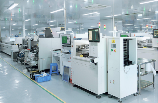
Manufacturing Techniques for High-Speed and High-Frequency PCBs
Precision Fabrication Techniques: Common and Unique Aspects
Precision is essential in the manufacturing of both high-speed and high-frequency PCBs. These boards require advanced fabrication methods to ensure optimal performance, especially when dealing with signal integrity, impedance control, and heat dissipation.
Laser Drilling and Microvias
Both high-speed and high-frequency PCBs rely on advanced drilling techniques, such as laser drilling, to create microvias. Microvias are small, high-density interconnects (HDI) that allow for compact PCB designs with multiple layers and small form factors.
High-speed PCBs often use microvias for routing data signals at fast rates across multiple layers, while high-frequency PCBs use microvias to handle high-frequency signals with minimal signal degradation. The size and aspect ratio of the vias, however, differ significantly between the two:
High-speed PCBs may use slightly larger vias to allow for more efficient signal flow at high data rates.
High-frequency PCBs, on the other hand, require smaller vias with tighter aspect ratios to avoid unwanted signal reflections and impedance mismatches, especially at frequencies above 1 GHz. Too large a via can cause signal attenuation and increased electromagnetic interference (EMI).
Surface Finish and Copper Quality
Surface finish and copper quality are critical to achieving reliable electrical performance in both high-speed and high-frequency circuits.
Copper Cladding for High-Speed and High-Frequency Performance
Copper cladding is the layer of copper that is bonded to the PCB to form the conductive paths for signals. For both high-speed and high-frequency applications, copper quality is a key factor in performance, but the specific needs differ slightly.
Electrodeposited (ED) Copper: Often used for high-speed PCBs, ED copper provides a smooth surface with good conductivity, making it suitable for fast signal transmission over short distances.
Rolled Annealed (RA) Copper: This type of copper is favored for high-frequency PCBs due to its smoother surface and lower surface roughness. The smoothness is important because surface roughness increases signal loss and reflection at high frequencies. RA copper also offers better signal integrity in high-frequency environments, reducing potential signal degradation.
Surface Finishes: ENIG, Immersion Gold vs. HASL
Surface finish refers to the final coating applied to the copper traces to protect them from oxidation and ensure good solderability. Different finishes can impact both signal quality and manufacturing reliability:
ENIG (Electroless Nickel Immersion Gold) and Immersion Gold are commonly used for high-frequency PCBs. These finishes offer smooth, flat surfaces that help minimize signal loss and provide superior conductivity, making them ideal for high-speed and high-frequency applications.
HASL (Hot Air Solder Leveling) is another surface finish commonly used in high-speed PCBs. While it offers a cost-effective solution and good overall performance, it may not be the best choice for high-frequency PCBs due to the rough surface texture that can contribute to signal degradation and EMI at higher frequencies.
Thermal Management and Power Distribution
Effective thermal management is a critical factor in the design of both high-speed and high-frequency PCBs. As circuits speed up or operate at higher frequencies, they generate more heat, which can affect performance and reliability.
Thermal Design for High-Power High-Speed Circuits
In high-speed PCBs, thermal design focuses on managing heat in high-power circuits that transmit large amounts of data at rapid speeds. Copper cladding and thermal vias are essential in conducting heat away from high-power components. Additionally, heatsinks or thermal pads are often added to help dissipate heat and prevent overheating that could lead to signal distortion or component failure.
Thermal vias are drilled holes filled with copper to transfer heat between different PCB layers. The number and placement of thermal vias must be carefully optimized to ensure efficient heat distribution and prevent hotspots.
Thermal Effects at High-Frequencies
For high-frequency PCBs, thermal management is equally important but presents additional challenges. Temperature variations at high frequencies can significantly impact the signal integrity of RF signals. For example, as the temperature changes, the dielectric constant of the materials can fluctuate, leading to impedance mismatches and signal distortion.
To address these challenges, temperature-stable materials such as PTFE-based laminates or ceramic composites are often used in high-frequency PCB designs. These materials maintain consistent dielectric properties over a wide temperature range, ensuring stable impedance and reliable performance even in extreme thermal conditions.
Testing and Quality Assurance for High-Speed and High-Frequency PCBs
Advanced Signal Integrity Testing
Signal integrity is a key factor in ensuring that high-speed and high-frequency PCBs function as intended, especially when operating at data rates above 10 Gbps or at frequencies above 1 GHz. Several advanced testing methods are employed to verify and enhance signal performance:
TDR (Time Domain Reflectometry) for Impedance Verification
TDR is one of the most widely used techniques for testing the impedance of high-speed and high-frequency PCB traces. By sending a signal through the PCB and measuring reflections caused by impedance mismatches, TDR helps to identify areas where signal reflection may occur, which can result in signal degradation or data errors. Ensuring that impedance is consistent across the board is critical to maintaining high-speed data integrity and minimizing signal loss in high-frequency designs.
TDR can pinpoint issues such as poorly matched vias, incorrect trace widths, or improperly positioned ground planes that could negatively affect the signal quality.
Eye Diagram Analysis: Signal Quality for High-Speed Circuits
Eye diagrams are a visual representation of signal quality in high-speed circuits. This method captures the shape of the signal over time, allowing designers to analyze characteristics like signal jitter, amplitude distortion, and timing errors. A clean "eye" in the diagram indicates optimal signal quality, whereas a closed eye suggests excessive noise, timing skew, or signal attenuation. This test is crucial in ensuring that high-speed data transmission remains error-free under various operating conditions.
Spectrum Analyzers: Signal Degradation and Interference
Spectrum analyzers are used to measure the frequency spectrum of high-frequency signals. This tool helps detect signal degradation and electromagnetic interference (EMI) that might be present in the PCB design. Spectrum analyzers are particularly valuable in identifying unwanted harmonics, noise, and cross-talk between traces, which can significantly impact high-frequency applications like RF circuits, 5G, and radar systems. By analyzing the spectrum, designers can adjust the layout to reduce interference and improve signal fidelity.
EMI and Crosstalk Testing for High-Frequency PCBs
High-frequency PCBs are more susceptible to EMI and crosstalk, which can disrupt signal integrity and cause performance issues in applications like communications, aerospace, and medical devices. Therefore, specialized testing methods are necessary to address these concerns:
EMI Shielding for High-Frequency PCBs
Electromagnetic interference (EMI) can cause signal degradation in high-frequency PCBs by introducing unwanted noise into the signal paths. Effective shielding is required to prevent EMI from affecting the performance of sensitive circuits.
Shielding can be achieved by adding ground planes, using conductive enclosures, or applying metallic coatings on the PCB. Shielding is especially critical for high-frequency applications such as 5G and radar systems, where even small amounts of interference can significantly impact performance. Testing the effectiveness of the shielding is done through EMI measurements, ensuring that the PCB meets regulatory standards and operates reliably in its intended environment.
Crosstalk Management: Reducing Noise Between Traces
Crosstalk occurs when signals from adjacent traces interfere with one another, especially in high-density designs. It is a common issue in both high-speed and high-frequency PCBs, but it is more pronounced in high-frequency applications due to the smaller trace widths and higher signal frequencies. Crosstalk can result in data errors or noise that corrupts the signal.
Managing crosstalk involves careful layout techniques, such as increasing the spacing between traces, using shielding between signal lines, or employing differential pairs for sensitive signals. Crosstalk testing ensures that traces are sufficiently isolated to prevent noise interference, especially in circuits where signal clarity is critical.
Reliability Testing for Both High-Speed and High-Frequency PCBs
Reliability is a major concern in high-speed and high-frequency PCB applications, where components are subjected to extreme conditions like temperature variations, vibration, and high operational stress. Comprehensive testing methods are employed to ensure long-term durability and functionality under challenging environments:
Thermal Cycling and Vibration Testing
Thermal cycling tests simulate the effects of rapid temperature fluctuations on PCB materials and components. This is particularly important for aerospace, automotive, and military applications, where the PCB may face extreme temperatures over time. The test ensures that the PCB can withstand repeated cycles of thermal expansion and contraction without causing component failures or delamination.
Vibration testing is also essential for PCBs used in aerospace and automotive environments. It ensures that the board can endure constant mechanical stress without signal loss or physical damage. Vibration tests check for weak solder joints or poorly secured components that may fail under real-world conditions.
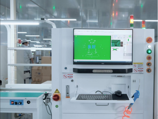
X-ray and Automated Optical Inspection (AOI)
X-ray inspection is a non-destructive method used to check for internal defects such as voids, misalignment, or soldering issues in multi-layer PCBs. This is particularly useful in high-frequency PCBs, where internal defects can cause signal degradation or impedance mismatches that are hard to detect through visual inspection alone.
Automated Optical Inspection (AOI) uses high-resolution cameras and computer algorithms to detect surface-level defects such as scratches, contamination, or incorrect component placement. AOI is essential for ensuring that high-speed and high-frequency PCBs meet the strict quality standards necessary for optimal performance. AOI can quickly identify areas of concern, allowing manufacturers to correct issues before they impact the final product.
Prototyping and Scaling Up Production for High-Speed and High-Frequency PCBs
Rapid Prototyping: Overcoming the Challenges of High-Speed and High-Frequency PCB Designs
Prototyping is an essential step for testing high-speed and high-frequency PCB designs before full-scale production begins. Given the specialized needs of these types of PCBs, prototyping must be fast, accurate, and capable of handling complex design features.
Prototyping in 24-48 Hours for High-Speed and High-Frequency Designs
In high-speed and high-frequency designs, where data rates and signal integrity are critical, prototyping must be quick to allow for fast iteration. Advanced manufacturing processes and technologies, such as laser drilling, HDI (high-density interconnect) techniques, and automated assembly, allow manufacturers to deliver working prototypes in as little as 24 to 48 hours.
The rapid prototyping process allows designers to evaluate the performance of high-speed circuits and high-frequency RF components before committing to mass production. In cases of failure or performance issues, this rapid turnaround time enables adjustments to be made quickly, reducing the overall development timeline.
Handling the Complexity of Multi-Layer High-Frequency Circuits in Prototype Testing
High-frequency PCBs often consist of multi-layer designs that require precise impedance control and signal routing. For example, the stack-up of layers must be carefully engineered to reduce signal loss and ensure electromagnetic compatibility (EMC).
Testing prototypes with multiple layers involves complex factors like via integrity, trace width consistency, and material selection (e.g., low-loss laminates like Rogers or Isola). Prototype testing ensures that the board performs optimally with minimal signal attenuation and that the RF signals maintain fidelity even as the design scales up.
Scaling Production: Ensuring Consistent Performance Across Large Runs
Once the prototype has been validated, the next step is to scale up production while maintaining the signal integrity and performance characteristics tested in the prototype phase. This requires a balance between maintaining high-quality standards and optimizing the manufacturing process for volume production.
Volume Production: Achieving Uniformity in High-Speed and High-Frequency PCB Designs
Scaling up production for high-speed and high-frequency PCBs presents the challenge of maintaining uniform performance across large production runs. Small discrepancies in via size, trace width, or material quality can affect signal transmission and lead to performance degradation, especially in high-frequency designs.
To ensure consistency in mass production, manufacturers rely on automated inspection tools like Automated Optical Inspection (AOI) and X-ray inspection to identify issues early in the production process. These tools allow for precise detection of defects such as misalignment, soldering issues, or trace imperfections, which can cause signal problems.
Strict quality control measures, such as automated testing (e.g., TDR and eye diagram analysis), ensure that each board produced meets the required impedance and signal quality standards.
Automated and Digital Workflows to Ensure Precision and Reduce Manufacturing Time
In high-speed and high-frequency PCB production, digital workflows and automation are critical for achieving precision and reducing lead times. CAD (computer-aided design) systems integrated with automated fabrication tools help streamline the entire manufacturing process, from design validation to component placement and soldering.
Digital fabrication technologies, such as laser etching and automated pick-and-place machines, help maintain the required precision for both high-speed data and RF signals. These technologies also enable real-time monitoring and adjustments during production, ensuring that each board is manufactured according to strict tolerances, even in high-volume runs.
Digital workflows also facilitate faster response times to changes in design or material specifications, ensuring that production stays on schedule and that the final products meet performance expectations.
Applications and Case Studies for High-Speed and High-Frequency PCBs
Telecommunications: 5G Networks and High-Speed Data Transmission
Telecommunications relies heavily on high-speed and high-frequency PCBs to support the latest advancements in communication technology. From 5G networks to fiber optic systems, these PCBs ensure high-performance data transmission and reliable connectivity across global networks.
Case Study 1: 16-Layer PCB for 5G Antenna Arrays
Design Challenges: Designing PCBs for 5G antennas involves managing complex mmWave (millimeter-wave) signals, which operate at extremely high frequencies (28 GHz and beyond). At these frequencies, traditional PCB materials and designs may introduce significant signal loss or reflection, undermining the performance of the communication system.
Solution: A 16-layer PCB was created to minimize insertion loss and provide precise impedance matching for the mmWave signals. Specialized low-loss materials, such as Rogers RO4350B laminate, were chosen for their ability to handle high-frequency signals with minimal attenuation. Additionally, microvia technology allowed for high-density interconnections while maintaining signal integrity.
Outcome: The 16-layer PCB enabled the deployment of 5G antennas that offered high data throughput with low insertion loss, ensuring seamless communication for 5G networks even at high frequencies.
Case Study 2: High-Speed Data Transmission in Fiber Optic Networks
Implementation: High-speed fiber optic networks require PCBs that can handle the high data rates of modern backbone communication systems. These PCBs are designed to maintain signal integrity over long distances and manage the speed of the data transfer.
Solution: High-speed multi-layer PCBs were implemented in the fiber optic transceivers and switching equipment. Advanced signal integrity tools, such as ANSYS HFSS simulations and TDR testing, were used to optimize trace impedance and reduce signal degradation.
Outcome: The PCB designs enabled high-performance data transmission, supporting the increasing demands of global communications infrastructure and maintaining optical signal integrity in high-speed data paths.
Aerospace: High-Frequency PCBs for Radar and Communication Systems
In the aerospace industry, high-frequency PCBs are critical for the design and operation of advanced radar systems, navigation equipment, and communication devices. These systems must perform reliably in environments with extreme conditions, including fluctuating temperatures, high altitudes, and mechanical stress. High-frequency PCBs ensure that signals are transmitted accurately and consistently, even in the most demanding aerospace applications.
Case Study 1: Civilian Aircraft Radar Systems
Design Challenges: Civilian radar systems in aircraft must be capable of detecting and tracking objects with precision while operating in environments that include extreme temperatures, vibrations, and high mechanical stress. The high-frequency circuits involved in these systems are highly sensitive to signal degradation, which can affect system accuracy and reliability. Moreover, maintaining signal clarity without interference is crucial for optimal radar performance, especially for navigation and collision avoidance systems.
Solution: High-frequency PCBs used in radar systems were designed with PTFE-based laminates such as Rogers RO4350B or Isola FR408HR, known for their low dielectric loss and ability to maintain stable impedance even under temperature fluctuations. The PCB designs also incorporated multiple layers and microvias to minimize signal loss and improve the efficiency of high-frequency signal transmission. Thermal cycling and vibration resistance were incorporated into the PCB design to ensure that it could withstand the stresses typically encountered during flight.
Outcome: The high-frequency PCBs allowed the radar systems to deliver precise, high-quality signals, ensuring reliable detection and tracking capabilities. These systems could perform under harsh environmental conditions, supporting the safety and operational efficiency of civilian aircraft.
Case Study 2: Satellite Communication Systems
Design Challenges: Satellite communication systems require high-frequency PCBs to handle RF signals in both uplink and downlink communications, often operating in the Ku-band or Ka-band frequencies (12–40 GHz). These systems are subjected to high-altitude conditions where temperatures and pressures vary significantly. Signal interference or attenuation could degrade the communication quality, especially when transmitting data over long distances to and from satellites.
Solution: For these systems, high-frequency PCBs were designed using specialized low-loss materials like PTFE and ceramic-based laminates to ensure minimal signal degradation during transmission. The boards were also designed to handle the high frequency of communication signals while maintaining stable impedance and minimizing crosstalk. The PCBs were tested to meet rigorous standards for thermal stability, vibration resistance, and electromagnetic shielding to protect against external interference.
Outcome: The high-frequency PCBs enabled seamless communication with satellites, ensuring reliable data transmission and clear signal reception. The low-loss materials helped achieve optimal performance in the harsh conditions of space, making them ideal for satellite communication systems used in global communication networks.
Medical Electronics: PCB Design for Imaging and Diagnostics
Medical electronics demand high-frequency PCBs that are not only capable of precise signal transmission but also need to meet stringent standards for signal clarity and reliability. Imaging systems like MRI scanners require PCBs that can handle sensitive signals with minimal electromagnetic interference (EMI).
Case Study: High-Frequency PCBs for MRI Systems
Design Challenges: MRI systems generate high-frequency signals that are critical to capturing detailed images of the human body. Any signal interference or signal degradation can affect image quality and diagnostic accuracy. Additionally, the size constraints of medical devices require compact, yet highly efficient, PCB designs.
Solution: The high-frequency PCB designed for the MRI system utilized low-loss laminates, such as Isola FR408HR, and precise impedance control to ensure minimal signal reflection and attenuation. The PCB also employed shielding techniques to prevent EMI from affecting the sensitive MRI sensors.
Outcome: The high-frequency PCB ensured high-quality images with minimal noise, improving the diagnostic capabilities of the MRI system and ensuring reliable, clear medical imaging for patients.
Conclusion
As the demand for faster, more reliable electronics continues to rise, the role of high-speed and high-frequency PCBs is more critical than ever. Next-generation materials such as ceramics and PTFE composites are paving the way for even higher performance, enabling low-loss transmission, stable impedance, and superior signal integrity in the most demanding environments. These innovations are essential for maintaining the integrity of high-frequency circuits in applications like 5G networks, satellite communications, and autonomous vehicles.
Looking ahead, the evolution of high-speed and high-frequency PCBs will be a driving force behind emerging technologies. As communications systems push toward higher data rates, automotive electronics demand more sophisticated systems, and aerospace seeks more robust radar and navigation solutions, the need for advanced PCB design and manufacturing will only grow. Companies like PCBMASTER, with extensive expertise in high-frequency and high-speed PCB design and production, are playing a crucial role in meeting these growing demands. With a focus on precision engineering and cutting-edge materials, PCBMASTER continues to deliver PCBs that meet the performance, durability, and reliability standards of the next generation of technology.
The future of high-speed and high-frequency PCBs is bright, offering unprecedented performance for a wide range of industries, and the continuous innovations in materials and design techniques will ensure these PCBs remain at the core of technological advancements for years to come.
FAQs
What is the difference between high-speed and high-frequency PCBs?
High-speed PCBs focus on handling data rates, typically above 10 Gbps. These designs are concerned with ensuring fast data transmission while minimizing signal loss, crosstalk, and delay across the board. They are commonly used in communications systems and high-performance computing.
High-frequency PCBs, on the other hand, are designed to handle radio frequencies (RF) typically above 1 GHz, used in applications like 5G networks, radar systems, and satellite communications. The primary concern for these designs is maintaining signal integrity and minimizing interference in high-frequency environments.
Key distinction: High-speed focuses on data throughput while high-frequency is concerned with operating at higher frequencies where signal loss and electromagnetic interference (EMI) become significant concerns.
Can I use standard FR4 for high-speed or high-frequency applications?
FR4 is a common PCB material, but it has limitations in both high-speed and high-frequency environments. For high-speed applications, FR4 can cause signal degradation and skew, especially at higher data rates, because it has a relatively high dielectric constant and loss factor. For high-frequency applications, the signal loss in FR4 becomes even more problematic, as it cannot adequately maintain impedance stability or handle the effects of electromagnetic interference (EMI) at frequencies above 1 GHz.
When to use specialized materials: For high-speed and high-frequency designs, it’s better to use low-loss laminates like Rogers RO4350B, Isola FR408HR, or PTFE composites, which are designed to handle high-frequency signals with minimal attenuation and stable impedance.
What are the challenges of testing high-frequency PCBs compared to high-speed PCBs?
Testing high-frequency PCBs presents different challenges compared to high-speed designs:
EMI Shielding: High-frequency PCBs are much more susceptible to electromagnetic interference (EMI), which can distort signals, so proper shielding is crucial during testing.
Signal Integrity at High Frequencies: High-frequency designs require careful impedance testing and verification of signal quality at microwave frequencies using tools like TDR (Time Domain Reflectometry) and vector network analyzers (VNA). At these frequencies, signal degradation and reflection can be more severe.
Crosstalk and Noise: High-frequency circuits also experience more noise due to their higher susceptibility to crosstalk between traces, requiring specialized testing to identify unwanted signal interference.
How does thermal management affect high-speed and high-frequency PCBs?
Thermal management plays a crucial role in ensuring the reliability and performance of high-speed and high-frequency PCBs:
High-speed applications generate heat due to the high data rates, which can cause signal distortion or component failure. Copper cladding, thermal vias, and heatsinks help dissipate the heat effectively.
High-frequency applications generate heat due to the power consumption of RF components. The high-frequency signals themselves can cause local heating on the PCB, and if not managed properly, this can lead to signal attenuation or even thermal damage to sensitive components.
In both cases, thermal vias, copper cladding, and heatsinks are used to distribute heat efficiently and maintain optimal performance. For high-power applications, active cooling methods may be required.
What is the role of impedance control in high-speed and high-frequency PCBs?
Impedance control is critical in both high-speed and high-frequency PCBs to ensure signal integrity and reduce signal loss or reflection:
High-speed PCBs: Impedance matching ensures that signals are transmitted with minimal reflection and that the high-speed data remains uninterrupted. It is usually maintained to ±5% tolerance using 3D electromagnetic simulations and testing techniques such as Time Domain Reflectometry (TDR).
High-frequency PCBs: Impedance control is even more important in high-frequency designs as higher frequencies are more susceptible to signal distortion and reflection due to small deviations in trace width or material properties. For RF signals, precise impedance matching is needed to prevent signal loss and to maintain stable signal transmission over long distances or in complex designs.
In both cases, tight impedance control ensures that the PCB’s traces match the desired impedance, reducing signal degradation, reflection, and other issues related to signal integrity.