


Populated Printed Circuit Boards vs. Bare PCBs: Key Differences Explained
In the world of electronics, a tiny board can make the difference between a device that works flawlessly and one that struggles to function. Some boards arrive empty, waiting for components to bring them to life, while others come fully equipped, ready to perform complex tasks the moment they leave the factory. Understanding how these two types of boards differ isn’t just for engineers—it’s key for anyone curious about how modern devices are built and why the right choice matters for performance, cost, and reliability.
Introduction to PCBs
What is a Printed Circuit Board (PCB)?
A Printed Circuit Board (PCB) is the foundation of most modern electronic devices. It mechanically supports and electrically connects electronic components using conductive pathways, also called traces, that are etched from copper sheets laminated onto a non-conductive substrate. PCBs are essential because they organize components in a compact and reliable layout, enabling devices to function efficiently.
A typical PCB consists of several basic components:
Substrate: The base material of the board, often made of fiberglass (FR4) or other insulating materials, providing structural support.
Copper Traces: Thin conductive lines that connect different components, acting as the board’s “wiring.”
Solder Mask: A protective layer that prevents accidental short circuits and protects traces from corrosion.
Silkscreen: Printed labels on the board that help identify components and assist in assembly.
Example: In a smartphone, a PCB serves as the backbone connecting the processor, memory, cameras, and other sensors. Without the PCB, these components could not communicate efficiently, and the device would not function.
Difference Between Bare and Populated PCBs
PCBs can exist in two main forms: bare and populated. Understanding the difference is crucial for designers, manufacturers, and hobbyists.
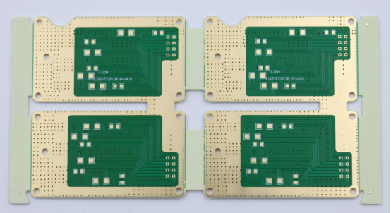
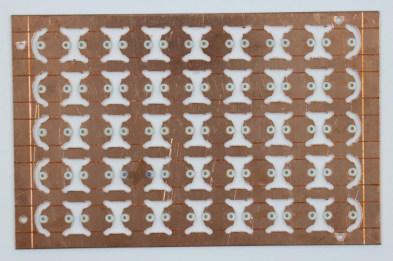
Bare PCB: This is a board that contains only the substrate, copper traces, solder mask, and silkscreen. It has no electronic components installed. Bare PCBs are typically used for prototyping, testing circuits, or educational purposes.
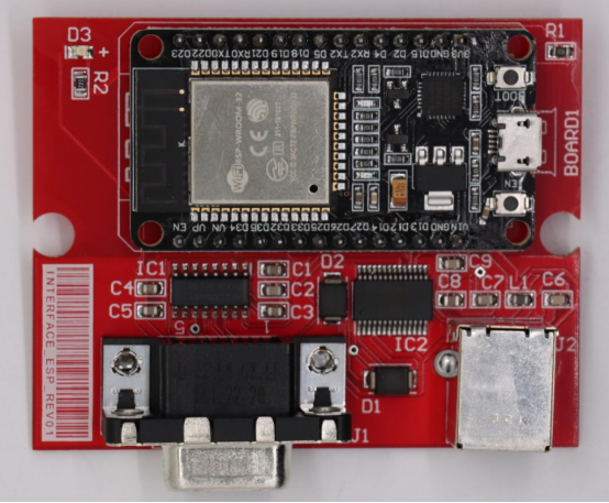
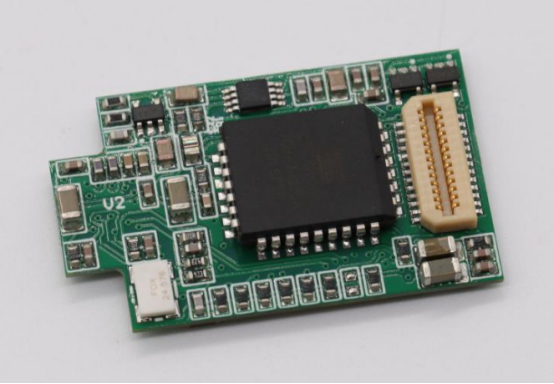
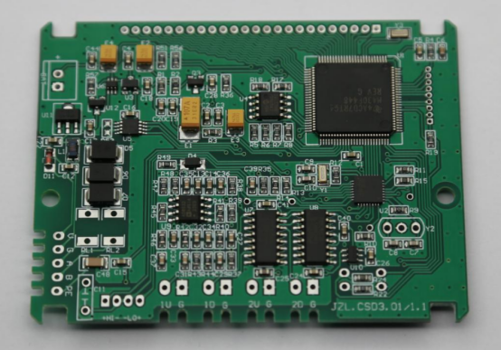
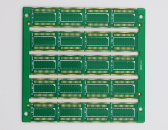
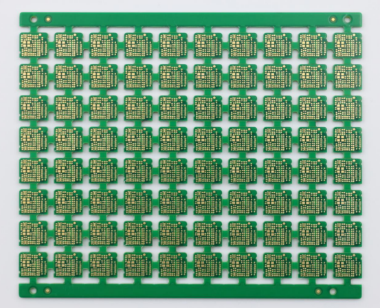
Populated PCB: Also known as an assembled or loaded PCB, this board has all required electronic components soldered onto it. Populated PCBs are ready for immediate use in devices, from consumer electronics to industrial machinery.
Quick Comparison Table: Bare vs Populated PCBs
Feature | Bare PCB | Populated PCB |
|---|---|---|
Components Installed | None | All required components |
Use Case | Prototyping, testing | Final product assembly |
Cost | Lower initial cost | Higher cost due to assembly |
| Readiness for Function | Non-functional | Fully functional |
| Complexity | Simple | More complex due to assembly |
By distinguishing between bare and populated PCBs, engineers can plan production, estimate costs, and ensure devices meet performance requirements. Even a small decision between the two can impact the efficiency, reliability, and scalability of electronic products.
Manufacturing Process of PCBs
Steps in Bare PCB Production
Producing a bare PCB involves several precise steps that ensure the board is ready for later component assembly.
Material Selection
The substrate is chosen based on mechanical strength, thermal stability, and electrical performance. Common materials include:
FR4: A standard fiberglass epoxy resin widely used for consumer electronics.
CEM-1: A paper-based material suitable for low-cost, simple boards.
Polyimide: High-temperature-resistant material used in flexible or high-performance PCBs.
Choosing the right material impacts durability, signal integrity, and production cost.
PCB Layering, Etching, Drilling, and Plating
Layering: Multiple layers of copper and substrate are stacked for multilayer boards.
Etching: Unwanted copper is removed to form the required circuit patterns.
Drilling: Precise holes are drilled for vias and component leads.
Plating: Conductive plating is applied inside drilled holes to create electrical connections between layers.
Example: A 4-layer bare PCB in a router will have signal, power, and ground layers precisely aligned and connected.
Quality Checks
Continuity Test: Ensures all intended electrical connections are complete.
Impedance Test: Confirms traces meet high-frequency signal requirements.
Visual Inspection: Detects defects such as scratches or misaligned layers.
Steps in Populated PCB Production
Once a bare PCB is ready, it can be transformed into a populated PCB by installing components.
1. Component Selection and Sourcing
Components include resistors, capacitors, ICs, connectors, and more.
Sourcing reliable parts ensures board performance and reduces production delays.
Example: Using automotive-grade ICs for a car’s electronic control unit ensures high reliability under harsh conditions.
2. Soldering Techniques
SMT (Surface Mount Technology): Components are placed on the board surface and soldered using reflow ovens.
Through-Hole Soldering: Components with leads are inserted into drilled holes and soldered, typically for high-stress parts.
Many boards use a hybrid approach, combining SMT and through-hole for optimal performance.
3. Testing
In-Circuit Testing (ICT): Checks individual component placement and electrical connections.
Functional Testing: Verifies that the assembled PCB performs its intended operation in real conditions.
Example: A populated PCB in a smartphone undergoes automated functional testing to ensure touchscreen and camera circuits work correctly.
Key Differences in Manufacturing
Manufacturing bare and populated PCBs differs in complexity, time, and cost.
Additional Complexity in Assembly: Populated PCBs require precise placement of components and careful soldering, increasing the risk of defects.
Lead Times and Costs Comparison:
Bare PCB: Faster production, lower cost, suitable for prototyping.
Populated PCB: Longer production time, higher cost due to assembly and testing.
Step-by-Step Example: From Bare PCB to Fully Populated Board
1. Start with a fabricated bare PCB.
2. Source and organize all required electronic components.
3. Apply solder paste and place components using pick-and-place machines.
4. Reflow soldering or through-hole soldering as required.
5. Conduct ICT and functional testing to ensure full operation.
6. Result: A fully populated PCB ready for integration into the final product.
Understanding these manufacturing steps helps engineers optimize design, cost, and production schedules while ensuring high-quality electronics.
Applications of Bare vs. Populated PCBs
When Bare PCBs are Used
Bare PCBs are primarily used in situations where the board itself, without components, is needed for testing, experimentation, or learning.
Prototyping and Testing: Engineers often use bare PCBs to test circuit designs before committing to full assembly. By working with just the traces and layers, they can quickly identify design flaws or routing issues without incurring the cost of components.
Educational Purposes: Bare PCBs are valuable in classrooms and labs where students learn electronics fundamentals. They allow hands-on practice in soldering, circuit tracing, and understanding board layouts.
Example: In an engineering lab, students might receive a bare PCB of a simple microcontroller board. They can then populate it with resistors, LEDs, and sensors themselves, learning how each component affects the circuit.
Bare PCBs are cost-effective, flexible, and ideal for iterative design processes or learning environments. They allow engineers and students to experiment without the risk of damaging expensive components.
When Populated PCBs are Used
Populated PCBs are used when a fully functional board is required for integration into a final product.
Final Product Assembly: Populated PCBs are assembled with all necessary components and are ready to be installed into devices like computers, smartphones, or industrial equipment.
High-Reliability Devices: Applications that demand high precision and durability, such as medical equipment, aerospace systems, and automotive electronics, rely on populated PCBs to ensure consistent performance.
Example: A laptop motherboard contains a densely populated PCB with processors, memory chips, connectors, and sensors soldered in place. This fully populated board allows the laptop to operate as intended immediately after assembly.
Populated PCBs reduce assembly time at the device level and minimize errors, ensuring the product is ready for deployment or sale. They are essential for high-volume manufacturing and applications where reliability is critical.
Performance and Reliability Considerations
Electrical Performance Differences
The electrical performance of a PCB depends heavily on whether it is bare or populated.
Impact of Components on Signal Integrity:
A populated PCB includes resistors, capacitors, and integrated circuits that shape how electrical signals travel through the board. These components influence signal integrity, controlling parameters like impedance, noise, and crosstalk. For instance, bypass capacitors can stabilize voltage and reduce interference in high-frequency designs.
In contrast, a bare PCB carries only copper traces without active or passive components, so it cannot regulate or amplify signals. It may show excellent raw conductivity, but without components, it cannot manage signal timing or filtering.
Comparison in High-Speed Circuits:
In high-speed circuits, populated PCBs perform significantly better because components like termination resistors and decoupling capacitors maintain clean signal transmission.
Bare PCBs, however, can be used for impedance testing and simulation during early design stages, helping engineers verify trace width and spacing before assembly.
Example: In a 10 Gbps data link, a bare PCB may demonstrate the designed impedance of 50 ohms, but only a populated PCB—with matching resistors and filters—ensures stable communication without reflection or jitter.
In summary, bare PCBs are used for electrical layout verification, while populated PCBs deliver actual circuit performance under real-world operating conditions.
Reliability Factors
The reliability of a PCB depends on its structural integrity and how it withstands mechanical, thermal, and electrical stresses.
Mechanical Stability:
Populated PCBs are generally more rigid because the attached components and solder joints add physical support and mass. Bare PCBs, while lighter, can flex more easily, making them less durable in environments with vibration or shock.
Failure Modes:
Bare PCB Failures: Typically occur from trace damage, delamination, or plating defects in vias. These failures usually result from manufacturing errors or mechanical stress.
Populated PCB Failures: Often arise from component failure, solder joint fatigue, or thermal stress during operation. Component aging or poor soldering can also degrade reliability over time.
Example: Vibration Testing Comparison:
In vibration testing, a bare PCB might show minor flexing or cracking at corner holes, while a populated PCB faces stress at solder joints and component leads. Engineers analyze both results to design boards that balance flexibility and strength—critical for applications such as automotive control units or aerospace electronics.
Overall, bare PCBs are easier to inspect for structural flaws, while populated PCBs require both mechanical and electrical reliability validation to ensure long-term performance.
Cost and Production Implications
Cost Factors for Bare PCBs
The cost of a bare PCB is primarily determined by materials, design complexity, and fabrication processes.
Material and Fabrication Costs:
The choice of substrate (such as FR4, CEM-1, or polyimide) affects the overall price. Standard FR4 boards are inexpensive, while high-performance materials like polyimide or Rogers add cost for their superior thermal and electrical properties.
Additional factors—such as the number of layers, trace width precision, and via types (blind, buried, or through-hole)—also influence fabrication expense.
Lower Upfront Cost for Prototyping:
Bare PCBs have lower initial costs because they exclude components and assembly labor. This makes them ideal for prototyping, circuit validation, or small-batch runs. Engineers can modify or test multiple board iterations quickly without committing to expensive assembly stages.
Example: A 4-layer FR4 bare PCB for a prototype might cost only $10–$15 per unit, while the same design, once populated, can exceed $80–$100 due to component and labor additions.
Cost Factors for Populated PCBs
A populated PCB incurs higher costs due to additional stages like component sourcing, assembly, and testing.
Component Cost and Labor/Assembly Cost:
Each resistor, capacitor, IC, and connector contributes to the total cost. Prices fluctuate based on availability and specifications—especially for specialized or high-tolerance components.
Assembly adds another major expense: SMT (Surface Mount Technology) and through-hole soldering require skilled labor or automated pick-and-place machinery. Setup time and rework can further increase the total.
Testing and Quality Assurance Expenses:
Every populated PCB undergoes multiple testing steps—in-circuit testing, functional testing, and automated optical inspection (AOI)—to ensure reliability. These processes require both time and specialized equipment, making the cost per unit higher than bare PCB fabrication.
Example: For a mid-complexity consumer electronics board, testing and quality control can represent 10–20% of total manufacturing costs, but they are essential for ensuring product reliability and minimizing warranty risks.
Cost-Benefit Comparison
The decision between producing a bare PCB and purchasing a populated PCB depends on production goals, volume, and timelines.
Step-by-Step Cost Example:
1. Bare PCB Fabrication: Material and process cost = $12 per board
2. Component Procurement: Components (resistors, capacitors, ICs, connectors) = $40 per set
3. Assembly Labor and Equipment: SMT placement, reflow, and inspection = $25 per board
4. Testing and Quality Control: Electrical and functional testing = $10 per board
Total Cost (Bare PCB + Assembly) = $12 + $40 + $25 + $10 = $87 per board
By contrast, ordering a pre-populated PCB directly from a contract manufacturer might cost $80 per unit, as bulk assembly and component sourcing reduce overhead.
Conclusion:
For small runs or prototypes, producing and assembling in-house can be more flexible.
For mass production, buying fully populated PCBs from an experienced manufacturer offers better cost efficiency and consistency.
Design and Customization Considerations
Design Flexibility
The design flexibility of a PCB depends largely on whether the board is in its bare or populated form.
Bare PCB: Ideal for Iterative Design Changes
Bare PCBs provide maximum design flexibility because they can be easily modified, tested, and re-fabricated during the development phase. Engineers can adjust trace layouts, layer configurations, or hole placements without the added complexity of mounted components.
This flexibility makes bare PCBs perfect for prototyping, circuit optimization, and design verification, especially when product requirements are still evolving.
Example: A hardware startup testing multiple sensor layouts might produce several versions of a bare PCB to refine trace routing and minimize noise before committing to full assembly.
Populated PCB: Design Locked Once Assembled
Once a PCB is populated with components, its design becomes fixed. Changing even a single component often requires reworking or redesigning the entire board. This is because soldered parts and precise component spacing make post-assembly modifications difficult and expensive.
As a result, populated PCBs are best suited for final, validated designs where the circuit has already passed all functional and performance testing.
Scalability
The scalability of PCB production determines how easily a design can transition from small-scale testing to mass manufacturing.
Populated PCBs: Essential for Mass Production
Populated PCBs are critical for high-volume manufacturing, where consistency, speed, and quality control are essential. Contract manufacturers can use automated SMT (Surface Mount Technology) and pick-and-place machines to assemble thousands of identical boards efficiently.
This scalability ensures uniform performance across all units and reduces per-unit cost over large production runs.
Example: In smartphone manufacturing, a single populated PCB design can be replicated millions of times with minimal variation, ensuring identical functionality in every device.
Bare PCBs: Best for Small-Scale Testing
Bare PCBs are more suitable for low-volume production, early testing, or educational use. They allow engineers to validate concepts before investing in automated assembly lines. Small design iterations can be made quickly and inexpensively, providing agility during product development.
Example: A research team developing a new IoT sensor may use ten bare PCBs to test different antenna configurations before scaling up with fully populated versions for pilot production.
In summary, bare PCBs excel in adaptability and experimentation, while populated PCBs deliver consistency and scalability—two complementary stages of the same product lifecycle.
Conclusion
Bare and populated PCBs serve different but equally important roles in electronics manufacturing. Bare boards are cost-effective and flexible, ideal for prototyping and early design validation, while populated PCBs deliver complete functionality, reliability, and readiness for final product integration. The right choice depends on your project stage, budget, and performance requirements. Whether you need precision bare boards or fully assembled PCBs, PCBMASTER—a professional PCB and PCBA supplier—offers reliable, high-quality solutions to help you move efficiently from prototype to production.
FAQs
Can a bare PCB be converted to a populated PCB at home?
Yes, a bare PCB can be converted to a populated PCB at home, but it depends on the circuit’s complexity. Simple boards with through-hole components can often be hand-soldered using basic tools like a soldering iron and multimeter. However, high-density or surface-mount (SMT) designs require precise soldering techniques, reflow equipment, and careful component handling. For complex or multi-layer boards, it’s best to rely on professional assembly services to ensure accuracy and performance.
How long does it take to assemble a populated PCB?
The assembly time varies based on board complexity and production method. A simple hand-soldered prototype might take a few hours to complete, while automated assembly for high-volume production can populate hundreds of boards per hour. Generally, professional PCB assembly — including soldering, inspection, and testing — can take anywhere from 1 to 5 days, depending on component availability and testing requirements.
Are populated PCBs more prone to failure than bare PCBs?
Populated PCBs are not inherently more prone to failure, but they do have more potential failure points because of the added components and solder joints. Bare PCBs, having no active parts, rarely fail unless physically damaged. In contrast, populated PCBs can experience issues such as component fatigue, solder joint cracking, or overheating during use. Proper design, high-quality soldering, and thorough testing minimize these risks and ensure long-term reliability.
What testing methods are used specifically for populated PCBs?
Populated PCBs undergo several specialized tests to ensure they function correctly:
In-Circuit Testing (ICT): Verifies that components are placed correctly and electrical connections are sound.
Functional Testing: Simulates real operating conditions to confirm that the board performs as expected.
Automated Optical Inspection (AOI): Uses cameras to detect soldering defects or misaligned components.
X-ray Inspection: Checks internal solder joints and hidden connections, especially for BGAs (Ball Grid Arrays).
These tests help detect both electrical and mechanical issues before the product reaches customers.
Can bare PCBs be reused or recycled?
Bare PCBs can sometimes be reused if they remain undamaged and free of solder residue, but it’s usually impractical for complex boards. Recycling, however, is common. Bare PCBs are often recycled to recover valuable materials like copper, gold, and fiberglass. Specialized recycling processes separate metal layers from non-conductive substrates, reducing electronic waste and promoting sustainability in PCB manufacturing.

