


PCBA Means: What It Really Stands for in Electronics
In the world of electronics, a seemingly simple board can carry the weight of an entire device’s functionality. Every smartphone, laptop, and smart gadget relies on a hidden layer of complexity that connects countless components into a cohesive system. Understanding what PCBA means is the first step to unraveling how modern electronics come to life, bridging the gap between raw circuit boards and fully functional devices.
Introduction to PCBA Means
What PCBA Stands For
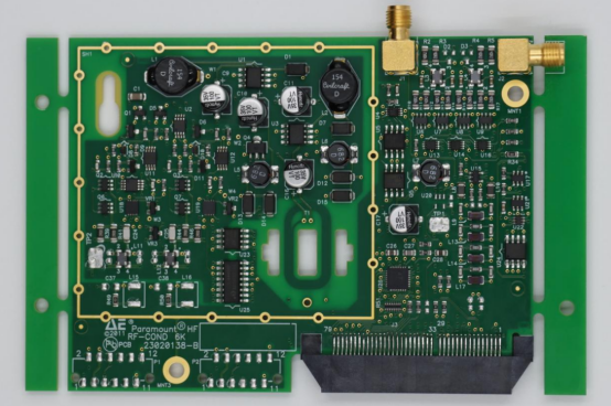
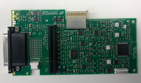
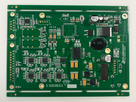
PCBA stands for Printed Circuit Board Assembly, which refers to a PCB that has all its electronic components soldered and interconnected to form a functional unit. In simple terms, while a bare PCB is just a board with copper traces, a PCBA is the complete electronic assembly ready to perform its intended function.
The word “Means” in this context highlights the practical significance of PCBA—it represents not just a physical board, but the entire system that enables electronic devices to operate. PCBA essentially means the stage at which a circuit board transforms from a passive substrate into an active, functional component of electronics.
Understanding what PCBA means is essential for anyone involved in electronics, whether professionals designing complex systems or hobbyists assembling simple gadgets. It helps in grasping how components interact, how signal paths are established, and why assembly quality directly affects device performance. For example, a misaligned component or poor soldering can cause the entire device to fail, which underscores the importance of proper PCBA practices.
Importance of PCBA in Modern Electronics
PCBA plays a central role in modern electronics by integrating multiple components onto a single PCB to create functional circuits. Each component—resistors, capacitors, ICs, and connectors—works together to carry out specific operations. This integration is what allows devices to become smaller, faster, and more reliable.
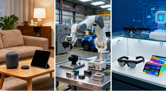
For instance, smartphones, laptops, and IoT devices all rely on PCBAs. In a smartphone, the PCBA connects the processor, memory, sensors, and wireless modules seamlessly, allowing the device to function as a compact, high-performance system. Similarly, IoT devices use PCBAs to combine sensors, communication chips, and power management circuits efficiently.
PCBA also impacts reliability, cost, and manufacturing efficiency. A well-designed assembly reduces the likelihood of component failure, lowers production costs by minimizing waste, and speeds up mass production. In short, PCBA is the backbone of electronic devices, bridging the gap between individual components and fully operational electronics.
Components and Materials of PCBA
Key Components on a PCBA
A PCBA consists of various components that work together to create a functional electronic circuit. These components can be broadly categorized into passive, active, and hardware elements.
Passive components include resistors, capacitors, and inductors. Resistors control the flow of current, capacitors store and release electrical energy, and inductors manage magnetic fields to regulate signals. These components do not generate power but play critical roles in shaping circuit behavior.
Active components are devices that can amplify, switch, or process electrical signals. Examples include integrated circuits (ICs), transistors, and diodes. ICs can contain thousands of tiny components inside a single chip, performing complex tasks such as processing, memory storage, or signal management. Transistors control current flow, while diodes ensure electricity flows in only one direction.
Additionally, PCBAs include connectors, switches, and other hardware that allow the board to interact with external devices or circuits. Connectors provide interfaces for power, data, or peripheral connections, while switches and buttons enable user input or control functions. Together, these components form a complete, functional assembly.
Materials Used in PCBA Manufacturing
The choice of materials in PCBA manufacturing significantly affects durability, performance, and signal integrity.
PCB substrates provide the structural base for all components. Common materials include FR4, a fiberglass-reinforced epoxy laminate ideal for most electronics; Rogers materials, which offer superior high-frequency performance for RF circuits; and flexible PCB materials, which allow bending and folding for compact or wearable devices.
Solder types are used to attach components to the PCB. Traditional leaded solder contains tin and lead, offering excellent wetting and mechanical strength. Lead-free solder meets environmental regulations but may require higher temperatures and careful handling.
Surface finishes protect the exposed copper on PCBs and ensure reliable soldering. Examples include HASL (Hot Air Solder Leveling), ENIG (Electroless Nickel Immersion Gold), and OSP (Organic Solderability Preservative). Each finish has its advantages: ENIG provides excellent surface flatness and long-term reliability, while OSP is cost-effective for simple assemblies.
For example, a high-frequency communication board using Rogers material and ENIG finish will maintain better signal integrity than a standard FR4 board with HASL. In contrast, a consumer gadget with low-speed circuits may perform perfectly with FR4 and OSP, offering cost savings without compromising functionality.
The PCBA Assembly Process
Step-by-Step Overview of PCBA Manufacturing
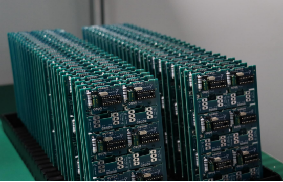
The PCBA manufacturing process transforms a bare PCB into a fully functional electronic assembly. Each step ensures that components are properly attached and the board meets quality standards.
1. Solder Paste Application
Solder paste is printed onto the PCB pads using a stencil. This paste contains tiny solder particles mixed with flux, which helps components adhere during soldering. Proper paste application is crucial, as an uneven or insufficient layer can lead to defects such as solder bridges or weak solder joints, impacting the overall reliability of the PCB.
2. Component Placement
Components are positioned onto the PCB using automated pick-and-place machines. These machines accurately place resistors, ICs, capacitors, and other components within millimeter tolerances. Compared to manual placement, this automated process is much faster and ensures higher precision, which is particularly important for high-density or complex boards.
3. Reflow Soldering
After components are placed, the PCB passes through a reflow oven where heat melts the solder paste. This process creates secure electrical and mechanical connections between the components and the board. Temperature profiles are carefully controlled during reflow to prevent damage to sensitive components, ensuring both functionality and reliability.
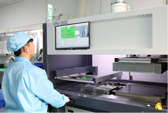
4. Inspection and Quality Control
Once soldering is complete, automated optical inspection (AOI) is performed to check for missing or misaligned components. For more complex assemblies, X-ray inspection is used to detect hidden solder defects, such as those under Ball Grid Array (BGA) packages. Finally, functional testing verifies that the board operates as intended before it is shipped to customers.
Differences Between Manual and Automated Assembly
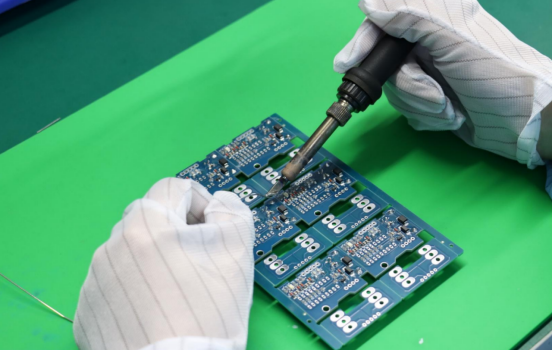
Manual soldering involves technicians hand-soldering components, often using a soldering iron.
Pros: Flexible for small quantities, prototypes, or repair work.
Cons: Slower, less consistent, higher risk of human error.
Automated assembly relies on machines for placement and soldering.
Pros: High precision, faster production, suitable for large-scale manufacturing.
Cons: Higher upfront cost and setup complexity.
Example: A startup producing a few prototypes may rely on manual assembly, while a smartphone manufacturer producing millions of units requires automated assembly lines for efficiency and consistency.
Common Challenges in PCBA Assembly
Even with careful manufacturing, some issues can occur:
Misalignment: Components placed incorrectly, potentially causing short circuits or failures.
Solder bridging: Excess solder connects adjacent pads unintentionally.
Cold joints: Poor soldering results in weak or intermittent electrical connections.
Step-by-step troubleshooting tips:
1. Inspect visually or with AOI to locate misaligned components.
2. Use rework stations or soldering irons to correct cold joints.
3. Adjust solder paste application and placement machinery to prevent recurring defects.
By understanding these challenges, manufacturers can reduce errors, improve reliability, and ensure that PCBAs function as intended in electronic devices.
Applications of PCBA in Electronics
Consumer Electronics
PCBA is at the heart of consumer electronics, enabling devices to function reliably and efficiently. In smartphones, PCBA connects processors, memory modules, cameras, sensors, and wireless communication chips to create a compact, high-performance device. Laptops rely on PCBAs to integrate CPUs, GPUs, storage, and connectivity interfaces, ensuring smooth operation and multitasking. Wearables such as smartwatches use PCBAs to combine small batteries, sensors, displays, and wireless modules in a miniaturized form factor.
In each case, PCBA ensures that components communicate correctly, power is managed efficiently, and the device performs as intended.
Industrial and Automotive Electronics
PCBA is equally critical in industrial and automotive electronics, where reliability and precision are paramount. Robotics use PCBAs to control motors, sensors, and communication systems. Automotive sensors rely on PCBAs to monitor vehicle performance, safety systems, and environmental conditions. Industrial controllers employ PCBAs to manage machinery, production lines, and process automation.
Compared to consumer electronics, industrial and automotive PCBAs are generally more complex and must withstand harsher conditions, such as extreme temperatures, vibration, and electrical noise. While consumer PCBAs prioritize compactness and cost-efficiency, industrial boards focus on durability, accuracy, and long-term reliability.
Emerging Technologies
PCBA plays a crucial role in emerging technologies that demand innovation and high performance. IoT devices use PCBAs to integrate sensors, wireless modules, and microcontrollers in small, low-power designs. Medical electronics, such as diagnostic equipment or wearable health monitors, rely on PCBAs for precise data acquisition and signal processing. Aerospace applications require PCBAs that can handle high-speed signals and extreme environmental conditions.
Current trends in these areas include miniaturization, enabling smaller and lighter devices, and high-speed signal boards, which support faster data transmission and real-time processing. PCBAs in these applications must balance size, power efficiency, and performance to meet evolving technological demands.
Key Terms Related to PCBA Means
PCB vs PCBA
A PCB (Printed Circuit Board) is a bare board with copper traces, designed to connect electronic components. It is the foundation of an electronic circuit but does not function on its own. A PCBA (Printed Circuit Board Assembly), on the other hand, is a PCB that has been populated with components such as resistors, ICs, and connectors, making it a fully functional unit.
Example / Step Comparison:
PCB stage: Only copper traces and pads are visible. No components are attached.
PCBA stage: Components are soldered onto the board, creating electrical connections. The board can now perform its intended function.
This distinction is critical for designers, engineers, and hobbyists to understand the stages of electronic assembly.
SMD vs Through-Hole Components
SMD (Surface-Mount Device) components are mounted directly onto the surface of a PCB. They are smaller, lighter, and suitable for high-density or miniaturized designs. SMD components are commonly used in smartphones, laptops, and wearables.
Through-hole components have leads that pass through holes in the PCB and are soldered on the opposite side. They offer stronger mechanical connections and are preferred for high-stress applications, such as connectors, power components, or boards exposed to vibration.
Example: For a compact smartwatch, SMD resistors and ICs are ideal to save space. For an industrial controller subject to mechanical stress, through-hole connectors provide durable and reliable connections.
High-Density and Multi-Layer PCBAs
High-Density Interconnect (HDI) PCBAs use finer traces, smaller vias, and multiple layers to achieve compact, high-performance designs. Multi-layer PCBAs can have 4, 6, or even more layers, enabling complex circuits in a small footprint.
Benefits:
Improved signal integrity for high-speed circuits.
Smaller board size for portable devices.
Ability to support more components and complex functionality.
Example: Modern smartphones and aerospace electronics rely on HDI PCBAs to integrate processing, memory, and communication modules without increasing the board size.
Troubleshooting and Best Practices
Common PCBA Failures
PCBAs can experience a variety of failures, often affecting device performance or causing complete malfunction. Some common types include:
Solder joint failure: Weak or cracked solder joints can interrupt electrical connections.
Component failure: Individual components like ICs, resistors, or capacitors may fail due to overvoltage, overheating, or manufacturing defects.
Trace breakage: Copper traces on the PCB can crack or break, disrupting the circuit path.
Step-by-step guide for identifying failure points:
1. Visual inspection: Look for obvious signs of damage, misalignment, or solder defects.
2. Electrical testing: Measure voltage, current, and resistance across suspected components.
3. AOI or X-ray inspection: Detect hidden defects such as cold joints or BGA issues.
4. Functional testing: Run the device to identify which part of the PCBA is not performing as expected.
By following these steps, engineers and technicians can pinpoint failure locations quickly and reduce downtime.
Tips for Reliable PCBA Design and Assembly
Ensuring PCBA reliability starts at the design phase and continues through assembly. Key practices include:
Proper component placement and orientation: Align components correctly according to polarity and datasheet specifications. Incorrect placement can cause shorts or failure.
Thermal management strategies: Use heatsinks, thermal vias, and proper spacing to prevent overheating of components, especially ICs and power devices.
Design for Manufacturability (DFM): Plan pad sizes, trace widths, and component spacing to facilitate automated assembly and minimize defects.
Example: When designing a power supply board, placing high-current components away from heat-sensitive ICs and ensuring proper solder mask coverage can improve longevity and reduce assembly errors.
Following these best practices not only improves the functional reliability of PCBAs but also reduces manufacturing costs and increases production efficiency.
Conclusion
PCBA, or Printed Circuit Board Assembly, is the process that transforms a bare PCB into a fully functional electronic system by adding components and creating electrical connections. Understanding PCBA is crucial for electronics professionals and hobbyists, as it affects device performance, reliability, and manufacturability. Key points include the types of components used, the assembly process, applications in consumer, industrial, and emerging technologies, and best practices for design and production.
For those looking to deepen their knowledge, exploring assembly guides, tutorials, and datasheets can provide practical insights. Related topics such as PCB design software, soldering techniques, and high-density board design are also valuable for further learning. For businesses and engineers seeking reliable solutions, PCBMASTER offers high-quality PCB and PCBA products, combining experience and expertise to ensure dependable performance for both prototypes and large-scale production.
FAQs
What PCBA Means in simple terms for beginners?
PCBA, or Printed Circuit Board Assembly, is a PCB that has all its electronic components attached and soldered, turning it into a functional electronic circuit. In simple terms, it’s what makes a bare circuit board “work” in a device, like a smartphone or wearable.
How does PCBA differ from a bare PCB?
A bare PCB is just the board with copper traces and pads; it cannot perform any function on its own. A PCBA is a PCB that has components like resistors, ICs, capacitors, and connectors mounted on it, making it a fully operational circuit ready for use.
What are the most common materials used in PCBA?
PCB substrates: FR4 (standard), Rogers (high-frequency), flexible materials (bendable boards).
Solder types: Leaded and lead-free solder for attaching components.
Surface finishes: HASL, ENIG, and OSP for protecting copper and improving solderability.
The choice of materials affects durability, signal integrity, and overall board performance.
Why is PCBA important in modern electronics manufacturing?
PCBA integrates multiple components into a single board, allowing devices to be compact, functional, and reliable. It impacts manufacturing efficiency, product quality, and cost. Without proper PCBA, electronic devices would fail to operate or be prone to defects.
How can I ensure quality in PCBA assembly at home or in small-scale production?
Use proper soldering techniques: Apply correct temperature and solder amount.
Check component placement and orientation: Ensure polarity-sensitive components are aligned correctly.
Inspect visually or with simple testing tools: Look for cold joints, misalignment, or bridging.
Follow small-scale assembly guides: Start with low-complexity boards before attempting high-density designs.

