


Mastering PCB High Precision Routing for Optimal Circuit Performance
Introduction
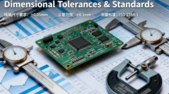
The difference of a millimeter can determine success or failure: In the field of precision electronics, the dimensional accuracy of a circuit board’s outline is as crucial as its internal circuitry. Precise molded dimensions are essential for circuit reliability, as even slight inaccuracies can compromise stable operation and long-term performance.
While most people focus on layer count, routing precision, and component integration density when evaluating PCB quality, one frequently overlooked yet critically important aspect is the PCB’s molded dimensions. Key factors such as molded dimensions, routing precision, and component integration density all contribute to high-precision routing.
So-called “molded dimensions” refer to the mechanically processed measurements of the PCB’s final outline, internal slots and cutouts, mounting holes, and gold fingers. While most designers concentrate on “electrical performance,” even minor deviations in these mechanical dimensions can cause disastrous outcomes during actual assembly. This article delves into why, in high-precision electronic devices, there’s zero tolerance for error in PCB molded dimensions.
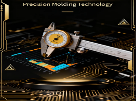
What Are High-Precision Molded Dimensions for Printed Circuit Boards?
PCB high-precision molded dimensions involve processing PCBs into specific shapes and structures with tight tolerances through CNC milling machines, laser cutting, or precision die punching.
These dimensions typically include:
·Overall Outline: The board's final length, width, and shape.
·Internal Slots and Cutouts: Non-circular openings used to accommodate heat sinks, connectors, or structural components.
·Mounting Holes: Screw holes used to securely fasten the PCB to enclosures or heat sinks with precision.
·Gold Fingers: Require precise chamfering and smooth edges to ensure smooth insertion into card slots.
High-precision molding typically demands tolerances controlled within ±0.10mm or even ±0.05mm, far exceeding the standard ±0.20mm tolerance for conventional PCBs.
Core Reasons: Why Are High-Precision Molded Dimensions Indispensable for Signal Integrity?

Ensuring Strict Assembly Compatibility and Interconnection Reliability
This represents the most direct and common reason. In many applications, the PCB doesn’t exist in isolation—it needs to interface precisely with enclosures, connectors, and other modules.
·Case in point: Gold finger cards: Components like graphics cards, network cards, and industrial control cards all insert into motherboard slots via gold fingers. If the board thickness or outline dimensions in the gold finger area exceed tolerances, it can lead to difficult insertion, poor contact, or excessive looseness causing disconnection during vibration. Precise chamfering and thickness control are prerequisites for maintaining stable connections through countless insertion cycles.
·Case in point: Enclosure assembly: In modern consumer electronics like smartphones and smartwatches, internal space is at a premium. The PCB must fit perfectly into the structure specifically designed for it. Oversized dimensions prevent installation, while undersized dimensions allow internal movement that can damage the device during drops.
Meeting Miniaturization and High-Density Integration Trends
As electronic devices become increasingly compact, the available space for PCBs leaves virtually no redundancy. Engineers maximize every bit of space in their designs.
A PCB with out-of-tolerance dimensions in miniaturized devices is like “wearing shoes one size too large”—it either won’t fit at all, forcing entire product batches to undergo structural redesign or scrapping, resulting in significant time and financial costs.
Enabling Effective Thermal Management
In many high-power devices (such as CPUs, GPUs, power modules), the PCB itself forms part of the thermal path. Heat transfers through mounting holes or specific areas on the PCB to metal enclosures or heat sinks.
If the positional accuracy or diameter of these mounting holes is imprecise, gaps form between the PCB and heat sink, preventing tight contact. This creates an air insulation layer between them, severely impeding heat conduction and causing chips to throttle performance or even fail due to overheating. High-precision molding ensures tight contact at thermal interfaces, forming the foundation for effective thermal design.
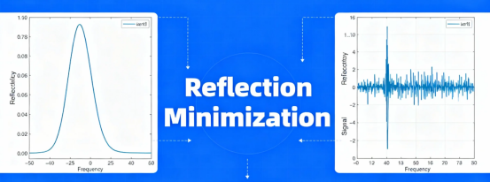
Guaranteeing High-Frequency/High-Speed Signal Integrity
This might be surprising, but mechanical structure indeed affects electrical performance. In fields like 5G communications, radar, and high-speed computing, signal frequencies are extremely high with very short wavelengths.
·Impedance continuity: The PCB’s outline edges, particularly near high-frequency transmission lines, affect the signal’s return path. Irregular board edges can disrupt impedance control continuity, introducing signal reflection and jitter. Improper routing on internal layers and outer layers can further exacerbate signal integrity issues, especially in complex multilayer PCB designs.
·Electromagnetic shielding: Some precision shields (EMI Cans) clip or solder onto specific grooves on the PCB. If molded dimensions are inaccurate, the shield won’t make proper contact with the board surface, causing electromagnetic leakage. The device becomes susceptible to external interference while potentially radiating excessive electromagnetic waves itself, leading to failure in EMC certification.
For high-frequency transmission lines, techniques such as using differential pairs are often employed to maintain signal quality and minimize signal integrity issues in high-speed designs.
Adapting to Automated Mass Production Requirements
Modern electronics manufacturing relies on highly automated pick-and-place machines and component inserters. These machines use fiducial marks and mounting holes on the PCB for accurate identification and positioning.
If molded dimensions vary between boards, the machines encounter deviations when grasping and positioning them. These deviations cause misalignment between component pads and solder paste during placement, triggering widespread solder bridging, cold joints, and other quality issues that severely reduce production yield. High-precision molded dimensions form the cornerstone of efficient, high-yield automated production.
PCB Stack-Up Design for High-Precision Routing
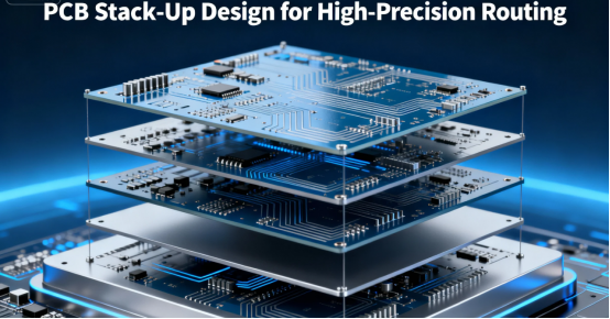
A well-planned PCB stack-up is foundational to achieving high-precision routing and optimal circuit performance. The arrangement of signal layers, power planes, and ground planes within the printed circuit board directly influences signal flow, heat dissipation, and the ability to maintain signal integrity. By carefully designing the stack-up, engineers can minimize electromagnetic interference (EMI) and ensure that critical signals are shielded from noise sources.
Proper PCB routing techniques, such as serpentine routing for length matching and differential pair routing for high speed signals, are most effective when supported by a robust stack-up. Controlled impedance is easier to achieve when signal layers are adjacent to continuous ground planes, reducing the risk of signal distortion and reflections. Following established PCB routing guidelines during stack-up design helps maintain uniform impedance and signal quality across the circuit board.
Additionally, a thoughtful stack-up enhances heat dissipation by strategically placing power planes and ground planes to act as thermal paths. This not only improves the reliability of the printed circuit board but also supports the overall signal integrity required for high-performance applications. By prioritizing stack-up design, engineers lay the groundwork for precise, reliable, and efficient PCB routing.
Trace Width and Spacing: Achieving Consistency and Performance
Selecting the appropriate trace width and spacing is essential for consistent and high-performance PCB routing. The trace width determines the current carrying capacity of each signal path, ensuring that electrical signals are transmitted safely without excessive voltage drops or overheating. At the same time, the spacing between traces plays a crucial role in minimizing electromagnetic interference and preventing signal distortion.
Proper PCB routing techniques require careful calculation of trace widths and spacing, often using advanced PCB design software to tailor these parameters to the specific needs of the circuit. Maintaining uniform impedance across all traces helps reduce signal reflections and ensures signal integrity, especially in high-speed or high-frequency designs. Incorporating buried vias and blind vias can further enhance routing density while minimizing the risk of crosstalk and signal quality degradation.
By adhering to established PCB routing guidelines and optimizing trace layouts, designers can achieve reliable, high-performance PCB designs that meet stringent electrical and mechanical requirements. Consistent trace width and spacing not only improve overall signal integrity but also contribute to the long-term reliability and manufacturability of the printed circuit board.
Signal Integrity Improvement in High-Precision PCB Routing
Signal integrity is a cornerstone of high-precision PCB routing, directly impacting the performance and reliability of the circuit board. To ensure that electrical signals reach their destination without degradation, designers employ a range of advanced PCB routing techniques. Differential pair routing is particularly effective for high speed signals, as it minimizes electromagnetic interference and enhances signal quality by ensuring that paired traces carry equal and opposite signals.
Length matching is another critical strategy, especially for clock signals and data lines, as it ensures that signals arrive simultaneously, reducing signal skew and timing errors. Impedance control throughout the routing process is vital for maintaining uniform impedance, which helps prevent signal reflections and distortion along the signal paths.
By following proper PCB routing guidelines and leveraging techniques such as controlled impedance and differential pair routing, engineers can significantly improve overall signal integrity. These practices are essential for achieving high-performance PCB designs that meet the demanding requirements of modern electronic systems.
Routing on Multiple Layers: Strategies for Precision and Reliability
As PCB designs become more complex, routing on multiple layers has become standard practice to accommodate dense component placement and intricate signal paths. However, multilayer routing introduces new challenges, particularly in maintaining signal integrity and minimizing electromagnetic interference.
To address these challenges, designers often route critical signals on inner layers, where they are shielded by adjacent ground planes and power planes. This approach reduces EMI and helps maintain consistent signal quality. Proper via placement and sizing are also crucial, as they ensure reliable electrical connections between layers without introducing unwanted parasitic effects.
Utilizing advanced PCB layout tools and auto routing features can streamline the routing process, improve manufacturing efficiency, and help manage the complexity of multiple layers. Strategic component placement, careful routing of clock signals, and robust power supply distribution further enhance the reliability and performance of the final PCB design.
By adhering to proven PCB routing techniques and guidelines, engineers can achieve precise, reliable, and high-performance circuit boards—even in the most demanding multilayer configurations.
Technical Challenges and Solutions for Achieving High-Precision Molded Dimensions and Impedance Control
Primary Challenges:
·Material characteristics: PCB substrates (like FR-4) comprise woven fiberglass and epoxy resin composites. Their anisotropic nature causes varying degrees of burrs and fiber tear-out during processing.
·Machining stress: Cutting bits generate stress on the board material during routing. Improper parameter settings easily lead to board warping or edge chipping.
·Coefficient of Thermal Expansion (CTE): Heat generated by high-speed tool rotation during processing can cause local material expansion, affecting final dimensional stability.
Key Technical Solutions:
·CNC milling and "secondary routing" process: Utilize high-rpm, multi-flute cutting tools with a "rough cut + finish cut" secondary routing process. The rough cut leaves excess material, while the finish cut makes the final precise trim in one pass, effectively enhancing edge quality and dimensional accuracy.
·Laser cutting technology: For particularly soft (like FPC flexible boards) or hard materials, laser cutting proves ideal. As a non-contact processing method, it eliminates mechanical stress, achieves precision up to ±0.03mm, and produces smooth, burr-free edges.
·High-precision molds: For high-volume, standard-shaped products, precision die punching offers the most efficient and consistent method. The mold's inherent high precision ensures uniformity of molded dimensions across every PCB.
Future Development Trends
With the growing adoption of System-in-Package (SiP), rigid-flex boards, and 3D molded circuit boards, demands for molding precision will become increasingly stringent. These complex board shapes often feature irregular 3D structures where molded dimensions not only affect planar assembly but directly determine their form and fit in three-dimensional space.
Laser Direct Imaging (LDI) and Automated Optical Inspection (AOI) technologies will see increased application in post-molding dimensional measurement, enabling fully digitalized process monitoring and feedback to ensure mechanical perfection in every critical PCB.
Conclusion
In summary, high-precision molded dimensions for PCBs are by no means a dispensable "cosmetic option." Rather, they represent a critical attribute intimately connected to an electronic product's assemblability, structural strength, thermal efficiency, signal quality, and production yield.
They form the bridge connecting the circuit design blueprint to the physical world. In today's pursuit of higher performance, smaller form factors, and more reliable applications, neglecting molding precision is like constructing a skyscraper on an unstable foundation. Therefore, when you next design or order a PCB for critical equipment, be sure to treat its molded dimension tolerances with the same seriousness as its electrical parameters—because this adherence to millimeter-level precision truly marks the dividing line between high-end manufacturing and ordinary production.
FAQs
Q. What factors affect the dimensional accuracy of PCB precision forming?
A. Panel fiducial mark issues: Blurry or misaligned fiducial marks can lead to inaccurate equipment positioning and deviation in the forming path.
Improper forming parameters: Deviations in V-scoring depth, excessive routing speed, etc., can all cause dimensional inaccuracies in the formed product.
Substrate deformation: Stretching of flexible PCB substrates or warping of rigid PCB laminates can result in dimensional deviations after forming.
Q. What are the requirements for fiducial marks to ensure high-precision forming dimensions?
A. Design: Use a "copper hollow circle" design, with the mark edge positioned ≥10mm from the panel edge.
Fabrication and Cleaning: Clean with isopropyl alcohol before prototyping; if blurred, remake using a laser engraving machine, with positioning deviation controlled within ±0.005mm.
Q. How to control forming parameters to ensure high-precision forming dimensions?
A. V-Scoring: Measure the actual PCB thickness before prototyping, set parameters according to "depth = actual thickness × 1/2", with depth deviation ≤ ±0.01mm; calibrate the cutting angle based on board thickness, with deviation ≤ ±0.5°.
Routing: Adjust routing speed according to the substrate: 300-500mm/min for FR-4 boards, 200-300mm/min for FPC boards; use a cutter diameter 0.2mm larger than the minimum forming dimension, calibrate the cutter after every 10 samples processed, with radial runout ≤ 0.002mm.
Q.What are the common dimensional tolerances for high-precision PCBs?
A. Generally, the dimensional deviation for high-precision PCBs is required to be within ±0.02mm. For some special high-precision PCBs, such as 6-layer PCBs, the outer dimensional tolerance can be controlled at +0.05/-0.15mm.
Q. How to solve the issue of edge chipping and burrs in PCB forming?
A. Optimize tool selection and maintenance: Use sharp-tungsten steel V-scoring blades, replace after every 50m of processing; use coated routing tools, inspect the blade after every 20 samples processed.
Adjust process parameters: Reduce V-scoring feed speed to 300-400mm/min for high-Tg FR-4 substrates; enable micro-lubrication when routing metal core boards; reduce routing speed by 20% for thick copper foil PCBs.
Author: Jack Wang

