


Etching Printed Circuit Boards: A Complete Guide to the PCB Etching Process
Etching lies at the heart of printed circuit board (PCB) manufacturing, transforming a simple copper-clad laminate into a precise network of conductive pathways. The process defines how accurately a circuit performs, influencing everything from signal speed and impedance control to overall product reliability. As electronic devices become smaller and faster, the demand for cleaner lines and tighter tolerances makes etching more than just a production step—it becomes a measure of technical capability.
From traditional ferric chloride solutions to advanced plasma and laser systems, the evolution of PCB etching reflects the industry’s constant pursuit of precision and sustainability. Understanding how copper is selectively removed, what materials are involved, and how process variables interact is essential for engineers, fabricators, and anyone aiming to achieve high-performance PCB results.
Introduction to PCB Etching
What Is PCB Etching?
PCB etching is the process of removing unwanted copper from a copper-clad laminate to form the desired circuit traces. During this step, only the copper protected by a photoresist or mask remains, while the exposed areas are chemically dissolved. The result is a precise pattern of conductive pathways that define how electrical signals travel through the board.
In simple terms, etching transforms a flat sheet of copper into a functional printed circuit. The process converts a blank substrate into a board capable of connecting components, transmitting signals, and providing power distribution. Without etching, a PCB would remain just a copper plate with no defined circuitry.
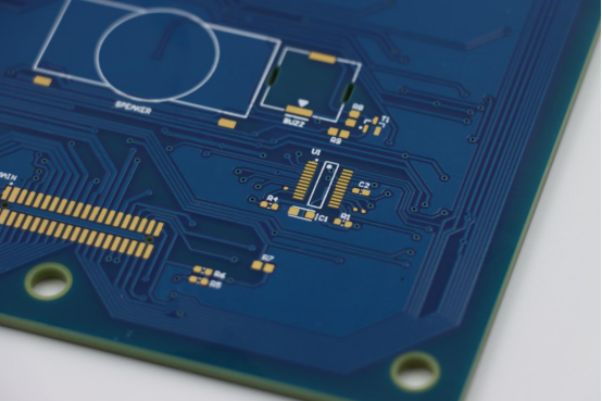
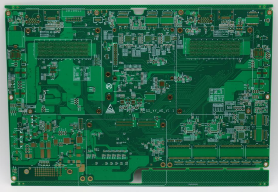
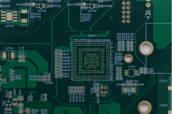
Etching also ensures electrical isolation between adjacent traces. Each trace must be accurately defined so that signals do not short-circuit or interfere with one another. In high-density circuits—such as those used in smartphones, servers, or aerospace systems—precise etching is essential for maintaining signal integrity and preventing crosstalk.
Why Etching Is Critical in PCB Manufacturing
Etching is one of the most critical stages in PCB production because it determines the final quality of copper traces. The depth and width of each etched line affect trace accuracy, impedance control, and signal reliability. Even minor deviations can cause high-speed signals to reflect or distort, reducing overall performance. For this reason, the etching process directly influences the electrical behavior of the entire circuit.
There are two main approaches to removing copper: chemical etching and mechanical etching.
Chemical etching uses acid-based or alkaline solutions (such as ferric chloride or cupric chloride) to dissolve copper selectively. It offers high precision and is widely used for multilayer and fine-pitch PCBs.
Mechanical etching, or milling, removes copper with physical tools or lasers. It’s often used for prototyping or rigid materials where chemical handling is less practical.
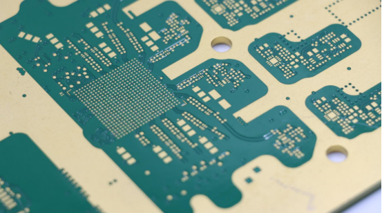
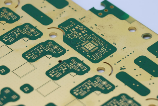
In multilayer, HDI (High-Density Interconnect), and fine-pitch designs, etching accuracy becomes even more important. These boards contain extremely thin traces and small gaps, often measured in microns. Controlled etching ensures that signal paths remain uniform across layers, preventing impedance mismatches and ensuring consistent performance in high-frequency or high-speed applications.
Understanding the PCB Etching Process
The Basic Principle of Etching
At its core, PCB etching is a controlled chemical process that dissolves unwanted copper while leaving behind the circuitry pattern protected by a photoresist layer. The reaction occurs when the exposed copper areas come into contact with an etchant—an acid or alkaline solution that oxidizes and removes copper molecules from the laminate surface.
The photoresist serves as a selective barrier. It’s applied and hardened over the copper areas meant to remain intact. When the board is submerged in an etching bath, only the uncovered copper reacts with the solution, while the protected regions stay intact. This contrast between exposed and masked zones allows for precise pattern formation, defining the electrical connections on the PCB.
Conceptually, the process can be broken down into three key steps:
1. Masking: A photoresist or dry film is applied and patterned using UV exposure to define the circuit layout.
2. Etching: The board is immersed in an etchant that dissolves exposed copper areas, creating isolated conductive traces.
3. Stripping: The photoresist is removed, revealing clean, accurately formed copper patterns ready for further processing.
This simple yet precise principle enables modern PCB manufacturers to create complex interconnects with micron-level accuracy.
Overview of Etching Methods
PCB etching can be carried out through wet chemical or dry (plasma) processes, each suited to different production needs and design complexities.
Wet Chemical Etching
Wet chemical etching is the most widely used method in PCB manufacturing. It employs liquid chemical solutions—commonly ferric chloride (FeCl₃), cupric chloride (CuCl₂), or ammonium persulfate ((NH₄)₂S₂O₈)—to remove unwanted copper.
These etchants chemically react with the exposed copper, converting it into soluble copper salts that are washed away during processing. Ferric chloride is preferred for prototyping and general production, while cupric chloride offers better regeneration capability for high-volume manufacturing.
Advantages:
High precision and consistent trace definition
Scalable for both small and large production runs
Compatible with multilayer and fine-pitch circuits
Disadvantages:
Generates chemical waste that requires careful neutralization and disposal
Sensitive to temperature and concentration variations, requiring strict process control
Dry Etching / Plasma Etching
Dry etching, also known as plasma etching, removes copper using ionized gases instead of liquid chemicals. In this process, a plasma composed of reactive gases (such as oxygen, chlorine, or fluorine-based compounds) bombards the exposed copper surface, gradually vaporizing it through physical and chemical reactions.
This method is particularly beneficial for HDI (High-Density Interconnect) and microvia structures where extreme precision and clean edges are essential. Because it eliminates liquid chemicals, plasma etching also reduces contamination and improves environmental safety.
Advantages:
Superior control and precision for micro-scale features
Environmentally cleaner and chemical-free
Ideal for thin substrates and fine-pitch designs
Disadvantages:
Slower and more expensive than chemical etching
Requires specialized vacuum equipment and process expertise
Comparison Table: Wet vs. Dry Etching
Aspect
Wet Chemical Etching
Dry / Plasma Etching
Process Medium
Liquid chemical solution (acidic/alkaline)
Ionized gas (plasma) Precision Level
High, but limited for very fine traces
Extremely high, suitable for microvias
Cost
Lower setup and operational cost
Higher due to specialized equipment
Speed
Fast, ideal for mass production
Slower, optimized for advanced designs
Environmental Impact
Generates chemical waste
Minimal waste, cleaner process
Best Use Case
Standard multilayer PCBs
HDI, microvia, and advanced microfabrication
Aspect
Wet Chemical Etching
Dry / Plasma Etching
Process Medium
Liquid chemical solution (acidic/alkaline)
Precision Level
High, but limited for very fine traces
Extremely high, suitable for microvias
Cost
Lower setup and operational cost
Higher due to specialized equipment
Speed
Fast, ideal for mass production
Slower, optimized for advanced designs
Environmental Impact
Generates chemical waste
Minimal waste, cleaner process
Best Use Case
Standard multilayer PCBs
HDI, microvia, and advanced microfabrication
In summary, both wet and dry etching share the same fundamental goal—precisely removing unwanted copper—but differ in execution, scalability, and precision. Wet chemical etching remains dominant in mainstream PCB manufacturing, while dry or plasma methods lead the way in next-generation high-density, high-frequency designs.
Step-by-Step Guide to Etching Printed Circuit Boards
Step 1 – Preparing the Copper-Clad Board
The first step in PCB etching is surface preparation. A clean, oxidation-free copper surface is essential for strong adhesion of the photoresist and accurate circuit definition. Any dirt, grease, or oxide layer can cause uneven etching or resist peeling during processing.
Use fine abrasive pads or microfiber polishing films to lightly sand the copper surface until it shines evenly. Then, wipe it with acetone or isopropyl alcohol using a lint-free cloth to remove remaining residues. Avoid touching the surface afterward, as fingerprints can introduce contaminants.
Proper cleaning ensures that the photoresist layer bonds uniformly to the copper, reducing defects such as pinholes and over-etching later in the process.
Step 2 – Applying and Developing Photoresist
Once the copper surface is prepared, a photoresist layer is applied to protect the areas of copper that will form the circuit traces. The photoresist acts as a barrier against the etchant.
There are three main types of photoresist coating methods:
Liquid photoresist, applied by spin-coating or dipping, offers flexibility for complex shapes.
Dry film photoresist, supplied as a roll or sheet, is laminated under heat and pressure for uniform coverage.
Spray coating is used in automated production for large or irregular boards.
After coating, the board is exposed to ultraviolet (UV) light through a photomask—a transparent film containing the circuit design. The UV light hardens the photoresist in the exposed areas, while the unexposed regions remain soft. During development, a mild alkaline developer dissolves the unexposed photoresist, revealing the copper pattern that will be etched away.
This step defines the circuit geometry with high precision and sets the foundation for clean, consistent etching.
Step 3 – Etching the Exposed Copper
The board is now ready for chemical etching, where the unwanted copper is dissolved to reveal the circuit design. The process takes place in an etching bath, which must be carefully controlled for temperature, agitation, and chemical concentration.
Common etchants include:
Ferric chloride (FeCl₃) – widely used for its reliability and availability.
Cupric chloride (CuCl₂) – preferred for industrial use due to its regenerative capability.
Sodium persulfate (Na₂S₂O₈) – produces cleaner edges and lighter residue, often used in prototyping.
In the chemical reaction, copper atoms are oxidized by the etchant and converted into soluble copper ions. The rate of etching depends on temperature (usually 40–50°C), solution concentration, and agitation to ensure even exposure.
Precise time control is essential—under-etching leaves excess copper between traces, while over-etching thins or breaks narrow lines. Process engineers often use test coupons to determine the ideal etching time before full production.
Step 4 – Stripping the Photoresist
After the etching step, the protective photoresist must be removed to expose the final copper traces. This process, known as stripping, ensures the surface is ready for solder mask application or further finishing.
Stripping is typically done using an alkaline solution such as sodium hydroxide (NaOH) or a solvent-based remover compatible with the photoresist type. The board is immersed or sprayed until all resist residues are dissolved.
It’s important to verify that no film or residue remains, as leftover material can interfere with solder mask adhesion or electrical testing. A quick rinse with deionized water ensures the surface is completely clean and neutralized.
Step 5 – Rinsing and Final Inspection
The final stage involves neutralizing and cleaning the board to remove any acid or chemical residues from the etching process. The board is rinsed thoroughly with deionized water and sometimes passed through a mild neutralization bath to balance surface pH.
After rinsing, the PCB undergoes optical inspection to check for defects such as over-etched lines, shorts, or incomplete copper removal. Automated Optical Inspection (AOI) systems may also be used in production environments for high precision.
Finally, a continuity test verifies that all traces are properly connected and isolated according to the design. A well-executed etching process results in clean copper patterns, sharp trace edges, and a flawless base for subsequent plating or solder mask steps.
Materials and Equipment Used in PCB Etching
Essential Chemicals
Successful PCB etching depends on choosing and handling the right chemical agents. Each chemical plays a specific role in removing copper, cleaning residues, or neutralizing acids after etching.
1. Etchants
The etchant is the primary chemical used to dissolve unwanted copper from the PCB surface. Common types include:
Ferric chloride (FeCl₃): A traditional and reliable etchant that works through oxidation. It produces strong, even etching but can stain surfaces and requires careful waste disposal.
Cupric chloride (CuCl₂): Regenerative and eco-friendlier than ferric chloride. It allows continuous reuse through oxidation control, making it suitable for large-scale manufacturing.
Hydrogen peroxide and hydrochloric acid (H₂O₂ + HCl): A fast-acting etchant often used in controlled environments. It provides clean results and is favored for precision applications but requires careful temperature and concentration management.
Each etchant has its own balance of speed, cost, and environmental impact. FeCl₃ is ideal for prototypes, CuCl₂ for production lines, and H₂O₂ + HCl for fine-feature PCBs requiring sharp trace definition.
2. Neutralizers and Cleaning Agents
After etching, residual acids must be neutralized to prevent corrosion or contamination. Common neutralizers include sodium bicarbonate (baking soda) or specialized alkaline solutions that stabilize pH.
Cleaning agents such as acetone, isopropyl alcohol (IPA), and deionized water are used throughout the process to remove grease, fingerprints, and chemical residues, ensuring smooth copper surfaces for subsequent layers.
3. Handling and Safety Considerations
Etching chemicals are corrosive and reactive, requiring strict safety measures. Always wear acid-resistant gloves, goggles, and a lab coat to prevent skin or eye contact. Use a fume hood or well-ventilated area to avoid inhaling vapors.
When mixing or diluting chemicals, always add acid to water—never the reverse—to prevent splashing or violent reactions. Proper labeling, storage in chemical-resistant containers, and neutralization before disposal are critical for safe and compliant operation.
Tools and Equipment
The efficiency and quality of PCB etching also depend on the tools and equipment used to control temperature, agitation, and exposure.
1. Etching Tanks and Agitation Systems
An etching tank is used to hold and circulate the etchant solution. It may be made of acid-resistant plastic or glass fiber composite and equipped with heaters and pumps.
Agitation—either mechanical or air bubbling—keeps the solution moving over the copper surface, ensuring even etching and preventing residue buildup. For consistent results, temperature (usually between 40–50°C) and solution flow rate must be precisely controlled.
2. UV Exposure Units
For photoresist-based etching, UV exposure units project ultraviolet light through a photomask to harden selected areas of the photoresist. Uniform exposure ensures accurate line definition, especially for fine-pitch and HDI PCB designs.
Modern UV systems feature digital timers and vacuum sealing to maintain even contact between the film and board, reducing pattern distortion.
3. Safety Gear and Ventilation Equipment
Since etchants emit fumes and can cause skin irritation, proper personal protective equipment (PPE) is non-negotiable. This includes rubber gloves, chemical-resistant aprons, and protective eyewear. A fume hood or local exhaust system minimizes exposure to acid vapors and chlorine gases that may form during etching.
4. Tips for Maintaining Consistency Across Batches
To ensure consistent results between production runs:
Regularly check etchant concentration using titration or density measurement.
Filter the solution to remove copper particles that may interfere with uniform etching.
Replace or regenerate spent etchant when etching speed slows or color changes.
Keep detailed process logs (temperature, time, agitation rate) to maintain repeatability across different batches.
Proper maintenance and calibration of tools not only improve product quality but also extend equipment lifespan and reduce chemical waste.
In short, the right combination of chemical control, precise tools, and disciplined handling practices defines the reliability of the etching process. Whether in a laboratory prototype setting or a high-volume factory, consistency and safety are the foundations of professional PCB etching.
Controlling Quality and Precision During Etching
Factors Affecting Etching Accuracy
The accuracy of PCB etching depends on a combination of chemical and mechanical factors that must be tightly controlled. Even small variations can lead to significant differences in trace width, copper thickness, and overall circuit reliability.
1. Temperature
Etching speed increases with temperature, but excessive heat can lead to over-etching—where copper is removed beyond the desired areas. Most chemical etching processes operate between 40–50°C, balancing efficiency and control. Consistent temperature ensures even reaction rates across the board surface.
2. Time
Etching time determines how deeply and completely copper is dissolved. Under-etching leaves thin copper films between traces, while over-etching erodes trace edges, reducing line width and current-carrying capacity. Process engineers often determine optimal timing through test coupons before mass production.
3. Agitation Rate
Proper agitation—using mechanical stirring or air bubbling—keeps fresh etchant in contact with the copper surface and removes reaction by-products. Insufficient agitation can cause uneven etching, while excessive turbulence may damage the photoresist. A steady, moderate flow achieves uniform results.
4. Etchant Concentration
The concentration of active chemicals (such as ferric or cupric ions) directly affects etching rate and uniformity. Weak or depleted etchant causes patchy results, while overly strong solutions attack protected areas. Regular titration tests or density measurements help maintain the correct chemical balance.
Inaccurate control of any of these factors can lead to asymmetric or incomplete etching, manifesting as rough trace edges or inconsistent copper thickness. Maintaining precise process conditions is the foundation of high-quality PCB manufacturing.
Common Etching Defects and How to Prevent Them
Even with precise control, certain defects can occur during PCB etching. Understanding their causes and prevention methods helps ensure consistent production quality.
1. Pinholes
Pinholes are tiny, unwanted holes that appear in copper traces. They often result from dust, oil, or moisture contamination on the copper surface before photoresist application. Prevention involves thorough cleaning, filtered air environments, and the use of lint-free materials.
2. Bridging
Bridging occurs when unwanted copper remains between adjacent traces, causing short circuits. It is typically caused by under-etching or insufficient photoresist adhesion. Regular inspection of etchant performance and consistent UV exposure help prevent this issue.
3. Line Width Variation
Variation in trace width happens when etching is uneven across the board. It may stem from temperature gradients, inconsistent agitation, or aging etchant solutions. To prevent this, manufacturers should monitor bath conditions, replace or regenerate etchant regularly, and verify photoresist uniformity.
4. Preventive Maintenance Practices
Maintaining chemical bath integrity and photoresist uniformity is critical. This includes:
Filtering etchant tanks to remove debris or copper particles.
Regularly checking solution density and pH levels.
Ensuring UV lamps in exposure systems are calibrated for consistent energy output.
Preventive maintenance minimizes downtime, stabilizes etching quality, and extends equipment lifespan.
Quality Inspection Methods
Once etching is complete, inspection and measurement confirm that all copper traces meet design tolerances and electrical requirements.
1. Microscopic Inspection
Using optical or digital microscopes allows operators to visually verify trace width, edge definition, and surface cleanliness. Microscopy is essential for detecting early defects like pinholes or micro-bridging that may not appear at first glance.
2. Cross-Section Analysis
In this technique, a small section of the PCB is cut and examined under magnification. Cross-section analysis reveals copper thickness, layer alignment, and etch depth consistency, providing a precise look at internal quality—especially for multilayer boards.
3. Automated Optical Inspection (AOI)
For high-density and fine-pitch circuits, Automated Optical Inspection (AOI) systems use cameras and algorithms to scan the PCB surface and compare it to design data (Gerber files). AOI detects missing traces, shorts, and dimensional deviations in seconds, ensuring that every board meets exacting standards before final processing.
In essence, precision in PCB etching is achieved through continuous monitoring, controlled variables, and thorough inspection. By understanding the sources of error and applying proactive quality control, manufacturers can deliver consistent, high-performance circuit boards that meet modern electronics’ stringent reliability demands.
Environmental and Safety Considerations
Handling Hazardous Chemicals
PCB etching involves chemicals that are corrosive, reactive, and potentially toxic, making proper handling critical for both worker safety and environmental compliance.
1. Personal Protective Equipment (PPE)
Always wear appropriate PPE when handling etchants, developers, or neutralizers. This includes:
Gloves resistant to acids and alkalis
Safety goggles or face shields to protect eyes from splashes
Chemical-resistant aprons or lab coats
Work in a well-ventilated area or under a fume hood to minimize inhalation of vapors.
2. Safe Storage and Labeling
Etchants and cleaning chemicals should be stored in acid-resistant containers with clear labels, away from heat sources or incompatible substances. Separate storage for oxidizers and acids prevents accidental reactions.
3. Guidelines for Mixing and Neutralization
When preparing or diluting solutions, always add acid to water, never the reverse, to prevent violent reactions. Spills should be neutralized immediately with baking soda or alkaline solutions. Proper handling protocols reduce the risk of chemical burns, gas release, or contamination of other materials.
Waste Disposal and Recycling
The etching process generates chemical waste and dissolved copper, which must be treated responsibly to meet environmental regulations.
1. Neutralization of Used Etchant
Spent etchant solutions are typically acidic or oxidative. Neutralization involves carefully adjusting the pH with alkaline substances such as sodium bicarbonate or sodium hydroxide until the solution reaches a safe, neutral level. This prevents environmental harm when discharging into wastewater systems.
2. Copper Recovery and Waste Minimization
Dissolved copper can be recovered through precipitation, electrolysis, or filtration systems. Recycling copper not only reduces environmental impact but also lowers material costs for manufacturers. Additionally, reusing etchant via regeneration methods helps maintain chemical concentration and extends bath life.
3. Eco-Friendly Alternatives and Sustainable Practices
Modern PCB manufacturing increasingly uses less hazardous etchants, such as organic or low-chloride solutions, which reduce chemical waste. Practices like closed-loop etching systems, waste recycling, and automation for precise chemical dosing further minimize environmental impact. Implementing these strategies supports sustainable production while maintaining high etching quality.
Advanced Etching Technologies
Etching in HDI and Multilayer PCBs
High-Density Interconnect (HDI) and multilayer PCBs require extreme precision during the etching process. Microvias, thin traces, and closely spaced features demand tighter control over etchant flow, temperature, and exposure time. Even minor deviations can lead to short circuits, open circuits, or impedance mismatches.
For multilayer boards, differential etching is often applied. Inner layers may use slightly longer etching times or stronger chemical concentrations to achieve uniform copper thickness, while outer layers require gentler etching to protect fine surface traces. This layered approach ensures that both inner and outer circuits meet design tolerances, enabling reliable signal transmission across the entire board.
Laser Etching and Plasma Etching Innovations
Modern PCB manufacturing increasingly relies on laser and plasma etching technologies to improve precision, speed, and environmental sustainability.
1. Laser Direct Imaging (LDI)
Laser etching systems, including LDI, directly expose the photoresist using focused laser beams. This method eliminates the need for photomasks, allowing ultra-fine trace patterns and rapid design iteration. LDI is particularly useful for microvias and high-frequency HDI boards, where micron-level accuracy is required.
2. Plasma Etching
Plasma or dry etching uses ionized gases to selectively remove copper, producing clean edges with minimal chemical waste. Unlike traditional wet etching, plasma methods reduce the consumption of corrosive solutions, lower environmental impact, and provide superior control over etch depth—critical for thin traces and multilayer interconnects.
Together, these technologies enhance both speed and yield, making them suitable for advanced electronic applications, from smartphones to aerospace systems.
Automation and Smart Process Control
Automation and AI-driven process monitoring are transforming PCB etching into a data-driven, highly controllable operation.
1. AI-Assisted Monitoring
Sensors integrated into etching tanks and exposure systems track temperature, agitation, chemical concentration, and etching progress in real time. AI algorithms can predict deviations, automatically adjust process parameters, and alert operators to potential defects before they occur.
2. Data-Driven Optimization
Collected process data enables manufacturers to refine etching recipes for higher yield, reduced material waste, and consistent trace quality. For example, AI can identify subtle trends in etchant degradation and recommend regeneration schedules, ensuring optimal performance across multiple production batches.
By combining advanced etching technologies with automation and smart monitoring, modern PCB manufacturers can achieve faster production, finer features, and more sustainable operations while maintaining strict quality standards.
Common Troubleshooting and Best Practices
Fixing Over-Etching and Under-Etching
Over-etching and under-etching are the most common defects in PCB fabrication, each with distinct causes and corrective measures.
1. Over-Etching
Causes: Excessive etchant strength, prolonged etching time, high temperature, or uneven agitation.
Identification: Traces appear thinner than design specifications, edges may be rough or uneven, and small lines could be partially removed.
Correction Methods:
Reduce etching time and monitor with a test coupon.
Adjust etchant concentration or replace spent solution.
Ensure uniform agitation and consistent temperature across the etching tank.
2. Under-Etching
Causes: Weak or depleted etchant, insufficient agitation, low temperature, or incomplete photoresist development.
Identification: Copper remains in areas where it should be removed, leading to bridging between traces.
Correction Methods:
Increase etching time gradually and monitor the process.
Check etchant concentration and regenerate or replace as needed.
Inspect photoresist adhesion and UV exposure quality.
Regular monitoring and small, incremental adjustments prevent repeat defects and maintain consistent board quality.
Maintaining Chemical Balance
Maintaining the chemical balance of the etchant is critical for predictable, uniform etching results.
Monitoring Methods:
Perform titration tests or density measurements to check active chemical concentration.
Track solution color, temperature, and reaction rate as visual indicators of etchant strength.
Replenishing Etchant:
Add fresh chemicals incrementally to maintain the target concentration.
Avoid sudden large additions, which can lead to uneven etching.
For regenerative etchants like cupric chloride, oxidation control and copper ion management help extend bath life.
Proper chemical maintenance prevents inconsistent etch rates and reduces the likelihood of over- or under-etching.
Process Optimization Tips
Optimizing the etching process ensures high-quality PCB production, minimizes waste, and improves yield.
Batch Consistency: Process each batch under the same controlled conditions to reduce variability. Label and log batch-specific parameters for traceability.
Temperature Control: Maintain stable etchant temperature using heaters or cooling systems. Avoid hot or cold spots that can create uneven etching.
Bath Agitation: Use mechanical stirrers, air bubbling, or recirculation pumps to keep the etchant in motion. Proper agitation ensures uniform copper removal and prevents localized over-etching.
Additional best practices include periodically filtering the etchant to remove debris, inspecting boards with test coupons, and keeping detailed process records. These measures collectively support repeatable, high-precision etching across production cycles.
With these troubleshooting and optimization strategies, PCB manufacturers can reduce defects, maintain chemical stability, and improve overall etching precision, even in high-density or multilayer designs.
Conclusion
Etching is a foundational process in PCB manufacturing, determining the accuracy of traces, signal integrity, and overall board reliability. Precision in temperature, etchant concentration, agitation, and exposure is essential for consistent results, especially in multilayer and HDI designs.
Advances like laser etching, plasma etching, and AI-assisted monitoring allow manufacturers to achieve finer features, faster production, and more sustainable operations. These modern techniques reduce waste and ensure every PCB meets strict design and performance standards.
Working with a reliable partner like PCBMASTER, which provides high-quality PCBs and PCBA services, makes implementing precise etching processes easier. Their expertise in advanced PCB solutions ensures that customers receive boards with accurate traces, consistent performance, and dependable quality, supporting both prototyping and large-scale production.
In summary, careful process control, quality inspection, and adoption of modern, sustainable etching methods are key to producing high-performance PCBs, and choosing a trusted supplier like PCBMASTER reinforces success at every step.
FAQs
1. What is the difference between ferric chloride and cupric chloride etching?
Ferric chloride (FeCl₃) is a widely used chemical etchant that oxidizes copper to dissolve it. It is reliable, easy to handle, and suitable for prototyping or small-scale production, but it generates more chemical waste.
Cupric chloride (CuCl₂) is regenerative, meaning it can be reused by controlling oxidation levels. It is preferred for large-scale manufacturing, offers more consistent etching rates, and reduces overall waste.
2. How can I safely dispose of used PCB etchant?
Neutralize spent etchants using alkaline solutions like sodium bicarbonate until the pH reaches neutral.
Recover copper through precipitation or electrolysis if possible, to minimize environmental impact.
Always follow local environmental regulations for chemical disposal and wear proper PPE during handling.
3. Which photoresist type is best for fine-pitch circuits?
Dry film photoresist or laser-direct imaging (LDI) compatible photoresist is ideal for fine-pitch circuits.
These options provide uniform thickness, high resolution, and sharp edges, enabling microvias and narrow traces with minimal defects.
4. Can PCB etching be done at home for prototypes?
Yes, small-scale PCB etching is possible using ferric chloride or ammonium persulfate in a controlled, ventilated environment.
Safety is critical: wear gloves, goggles, and a mask, avoid spills, and work in a space with proper ventilation.
Home etching is typically suitable for single-layer prototypes and hobby projects, not advanced multilayer HDI boards.
5. What causes uneven copper removal during etching?
Uneven etching is usually caused by temperature fluctuations, inconsistent agitation, depleted etchant, or poor photoresist adhesion.
Areas with slower chemical flow or thicker resist may remain under-etched, while stagnant spots or overexposed edges may experience over-etching.
Maintaining uniform bath conditions, proper agitation, and fresh chemicals helps ensure consistent copper removal.

