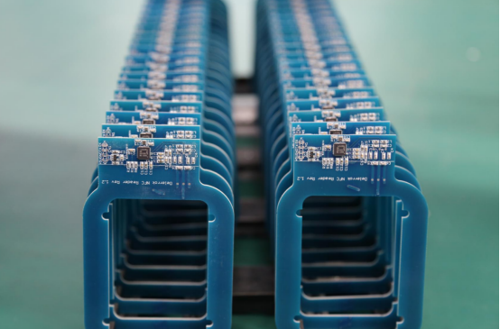
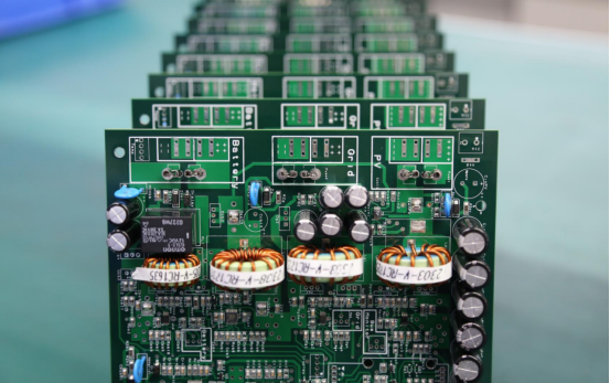
PCBA Circuit Board: Everything You Need to Know About Modern Electronics
In today’s fast-paced digital world, the tiny circuits inside our devices determine how efficiently and reliably they operate. The PCBA (Printed Circuit Board Assembly) circuit board plays a crucial role in connecting and coordinating electronic components, enabling everything from smartphones to automotive systems to function seamlessly. These compact assemblies combine precise design, advanced materials, and meticulous manufacturing to meet the demands of modern electronics.
Introduction to PCBA Circuit Boards
What is a PCBA Circuit Board?
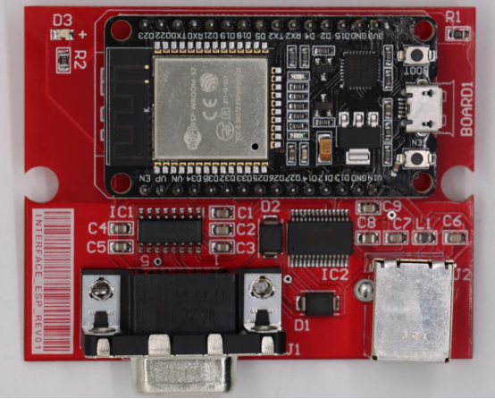
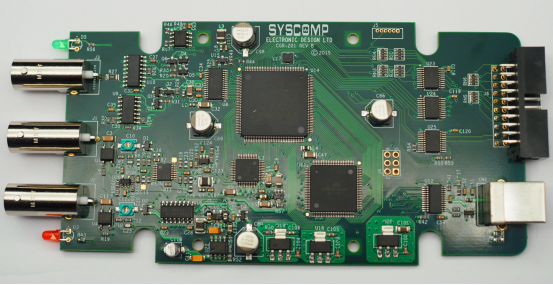
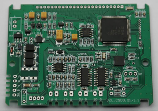
A PCBA (Printed Circuit Board Assembly) is a printed circuit board (PCB) that has electronic components mounted and soldered onto it, forming a functional electronic circuit. Unlike a bare PCB, which is just a flat board with conductive traces, a PCBA includes all the active and passive components needed to perform its intended function.
The key difference between a PCB and a PCBA is that a PCB is the structural base for circuits, while a PCBA is the fully assembled board ready to operate. For example, a bare PCB may have copper traces and holes, but it cannot process signals or power devices until components such as resistors, capacitors, and integrated circuits (ICs) are added.
Key components of a PCBA include:
Resistors: Control the flow of electric current.
Capacitors: Store and release electrical energy.
Integrated Circuits (ICs): Perform complex processing or logic functions.
Connectors: Provide interfaces for power and signal connections.
Example: A bare PCB for a smartphone may look like a flat, patterned board with copper traces, but the fully assembled PCBA includes tiny ICs, sensors, and connectors, allowing the smartphone to operate.
Importance in Modern Electronics
PCBAs are essential in virtually all modern electronic devices. In consumer electronics, they enable smartphones, laptops, and smart home devices to function efficiently. In automotive systems, they control everything from engine management units to infotainment systems. In telecommunications, they support high-speed signal transmission in routers, switches, and mobile networks.
The quality of a PCBA directly affects device performance and reliability. A well-designed PCBA ensures stable electrical connections, minimizes signal loss, and prevents overheating, while a poorly assembled board can lead to device failures, shorter lifespans, or safety risks.
Example: A smartphone with high-quality PCBAs may last several years without performance issues, while one with low-quality assemblies may experience battery problems, screen malfunctions, or connectivity failures within a short period.
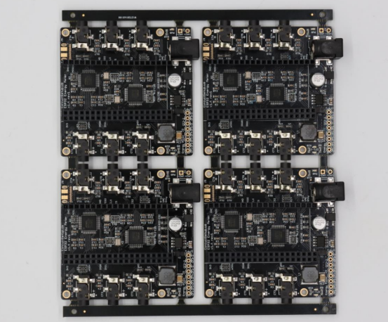
PCBA Manufacturing Process
PCB Design and Fabrication
The PCB design and fabrication process is the first step in creating a functional PCBA. It typically follows three main stages:
1. Schematic Design: Engineers create a circuit diagram that defines the electrical connections between components.
2. PCB Layout: The schematic is translated into a physical layout, specifying the placement of components and the routing of copper traces.
3. Fabrication: The board is manufactured using layers of conductive material and insulating substrates, drilled, and plated to prepare for assembly.
Common PCB materials include:
FR4: Standard, cost-effective laminate for general electronics.
Rogers: High-frequency laminate suitable for RF and microwave circuits.
High-speed laminates: Optimized for low signal loss and impedance control.
Example: A multilayer PCB used in a high-frequency router may have 8–12 layers of traces and planes, reducing signal interference and supporting fast data transmission.
Component Sourcing and Preparation
Before assembly, all components must be sourced and prepared.
BOM (Bill of Materials) Creation: Lists every component, including values, tolerances, and part numbers.
Component Sourcing: Manufacturers choose between OEM (Original Equipment Manufacturer) components for higher reliability or aftermarket components for cost savings.
Example: For precision electronics, low-tolerance resistors and capacitors are selected to ensure consistent performance, especially in high-speed circuits or sensitive measurement devices.
Assembly Techniques
PCBA assembly involves mounting and soldering components onto the PCB. The two main techniques are:
SMT (Surface Mount Technology): Components are placed directly onto the surface of the board. It allows smaller components and higher component density.
Through-Hole Technology (THT): Component leads are inserted into pre-drilled holes and soldered on the opposite side. THT provides stronger mechanical connections.
Step-by-step soldering process (for SMT):
1. Apply solder paste to pads using a stencil.
2. Place components using automated pick-and-place machines.
3. Reflow soldering in an oven melts the paste, creating secure connections.
Comparison of SMT vs. THT:
SMT: High density, faster production, suitable for compact electronics.
THT: Strong mechanical support, ideal for connectors or heavy components.
Testing and Quality Assurance
Quality assurance ensures each PCBA functions reliably.
In-Circuit Testing (ICT): Checks individual components and connections for electrical correctness.
Functional Testing: Verifies the entire board performs as intended under real conditions.
Automated Optical Inspection (AOI): Uses cameras to detect soldering defects, misaligned components, or missing parts.
Example: AOI can identify a tiny solder bridge between two pins on a microcontroller, preventing failures before the PCBA reaches the customer.
PCBA Design Considerations
Electrical Design Factors
Electrical design is critical to ensure a PCBA functions reliably at high speeds. Key considerations include signal integrity, impedance matching, and EMI (electromagnetic interference) mitigation.
Step-by-step guide for routing high-speed traces:
1. Identify high-frequency signal paths on the schematic.
2. Route differential pairs together, maintaining consistent spacing for impedance control.
3. Minimize trace length to reduce signal delay and reflections.
4. Avoid sharp corners; use 45° angles or curved traces to maintain signal integrity.
5. Place ground planes strategically to shield sensitive traces and reduce EMI.
Example: In USB or HDMI circuits, differential pair routing ensures the signals remain synchronized, minimizing crosstalk and data errors.
Mechanical and Thermal Considerations
Mechanical and thermal design affect both durability and performance. PCB thickness, hole sizes, and layer stacking must be optimized for structural stability and manufacturability.
Thermal management strategies include:
Using heat sinks to dissipate energy from high-power components.
Employing thermal vias to transfer heat between layers.
Incorporating copper planes to spread heat evenly across the board.
Example: A PCBA for a high-power LED module may include multiple copper layers and thermal vias to prevent overheating, ensuring stable light output and long component life.
Cost and Manufacturing Constraints
Design decisions directly impact manufacturing feasibility and production costs. Engineers must balance complexity with manufacturability, avoiding overly intricate designs that are hard to produce.
Key considerations:
Reducing unnecessary via counts to lower fabrication costs.
Choosing standard PCB sizes to minimize custom tooling.
Evaluating component placement for efficient assembly.
Considering lead times for mass production, including component availability and supplier reliability.
Example: By reducing the number of blind or buried vias in a multilayer PCB, a manufacturer can save both time and cost, while maintaining signal performance.
PCBA Applications Across Industries
Consumer Electronics
PCBA plays a central role in consumer electronics, powering devices that people use every day, such as smartphones, laptops, and wearable devices. These boards enable compact, efficient, and high-performance circuits that support advanced functionality.
Example: In smartwatches, miniaturized PCBAs integrate sensors, processors, and wireless modules within a tiny form factor, allowing features like heart-rate monitoring, GPS tracking, and notifications without increasing device size.
Automotive Electronics
In the automotive industry, PCBAs are critical for modern vehicle functionality. They are used in Engine Control Units (ECUs), various sensors, and infotainment systems, providing precise control and communication throughout the vehicle.
Example: Autonomous vehicles rely on high-reliability PCBAs for sensor modules, including LIDAR and radar units. These PCBAs must withstand extreme temperatures, vibration, and electromagnetic interference to ensure safe and accurate vehicle operation.
Industrial and Medical Equipment
PCBAs are essential in industrial automation and medical equipment, where reliability and precision are paramount. In industrial settings, PCBAs drive robotics, factory automation, and control systems, improving efficiency and reducing human error. In medical devices, PCBAs power diagnostic equipment, imaging systems, and monitoring devices, where precision and uptime are critical.
Example: MRI machines use PCBAs to control imaging sensors and data acquisition circuits, while automated assembly lines rely on PCBAs to manage robotic arms and process sensors, ensuring high productivity and accuracy.
Innovations and Trends in PCBA
Advanced Materials and Technologies
Modern PCBAs increasingly use advanced materials to meet higher performance requirements. Common innovations include high-frequency laminates, flexible PCBs, and HDI (High-Density Interconnect) technology. These materials and designs enable faster signal transmission, reduced board size, and higher component density.
Step-by-step benefits of switching to flexible PCBA:
1. Space savings: Flexible boards can bend or fold, allowing compact device designs.
2. Improved reliability: Fewer connectors reduce potential points of failure.
3. Weight reduction: Flexible PCBs are lighter than rigid multilayer boards.
4. Dynamic applications: Suitable for wearable electronics, foldable devices, and automotive sensors that require movement.
Example: A foldable smartphone uses flexible PCBAs to maintain electrical connections across moving parts, enabling smooth folding without damaging circuits.
Automation and AI in PCBA Manufacturing
Automation and AI are transforming PCBA production, improving speed, accuracy, and quality.
Robotics in assembly lines: Automated machines place components with high precision, reducing human error and increasing production throughput.
Predictive quality assurance (QA): AI-driven systems analyze data from soldering, placement, and inspection processes to predict defects before they occur, allowing proactive corrections.
Example: An AI-powered assembly line can detect a misaligned microchip in real time, automatically adjusting placement settings and preventing defective boards from reaching customers.
Sustainability in PCBA Production
Sustainable practices are becoming a priority in electronics manufacturing. Key approaches include lead-free soldering and using recyclable or eco-friendly materials to reduce environmental impact.
Example: Some manufacturers implement green PCBA initiatives by using biodegradable substrates and lead-free solder alloys, minimizing hazardous waste while maintaining high performance and reliability.
Troubleshooting and Maintenance of PCBA
Common Failures and Causes
PCBAs can fail due to several common issues, often impacting device performance or causing complete malfunction. Key failures include:
Solder joint cracks: Caused by mechanical stress, thermal cycling, or poor soldering.
Component burnout: Overheating or electrical overload can damage resistors, capacitors, or ICs.
PCB delamination: Moisture absorption or excessive heat can separate PCB layers, disrupting connectivity.
Example: A smartphone experienced repeated shutdowns because the PCBA in its power management module developed solder joint cracks from repeated thermal cycling, highlighting the importance of thermal stress management in design.
Repair Techniques
Repairing PCBAs requires precision and careful handling. Common techniques include:
Component replacement: Removing faulty components and soldering new ones.
Reflow soldering: Applying controlled heat to remelt solder, restoring electrical connections.
PCB rework: Adjusting or repairing traces, vias, or pads on the board.
Step-by-step guide for small-scale PCBA repair:
1. Identify the faulty component or connection using visual inspection or testing tools.
2. Remove the defective component carefully, avoiding damage to nearby parts.
3. Clean the pad or solder area to remove residual solder.
4. Place the new component and secure it using soldering or reflow techniques.
5. Test the repaired PCBA to ensure proper functionality.
Preventive Measures
Preventive measures help extend PCBA life and reduce failure rates. Key practices include:
Proper storage: Keep PCBAs in anti-static, moisture-controlled environments.
Thermal management: Use heat sinks, thermal vias, and copper planes to dissipate heat efficiently.
Handling precautions: Avoid mechanical stress or electrostatic discharge during assembly and maintenance.
Example: Applying a conformal coating to moisture-sensitive electronics protects the PCBA from humidity, dust, and chemical contamination, improving reliability in harsh environments.
Conclusion
High-quality PCBA (Printed Circuit Board Assembly) is crucial for the performance, reliability, and lifespan of modern electronic devices. From smartphones and laptops to automotive systems and medical equipment, PCBAs ensure precise signal transmission, control, and overall device functionality. Proper design, material selection, assembly techniques, and quality control help prevent failures and maximize efficiency.
The future of PCBA design is driven by flexible PCBs, high-density interconnects, and AI-assisted manufacturing, enabling smaller, faster, and more reliable boards. At the same time, sustainable practices such as lead-free soldering and recyclable materials are becoming standard in electronics manufacturing.
Achieving these standards requires experience and technical expertise. PCBMASTER, with years of experience in PCB and PCBA design and manufacturing, offers advanced solutions ranging from high-speed multilayer boards to custom assemblies. Their capabilities ensure that modern electronics meet both performance and reliability requirements while keeping pace with technological innovations.
Partnering with skilled manufacturers like PCBMASTER allows companies to deliver durable, high-performance, and forward-looking electronic products, turning advanced PCBA designs into real-world applications.
FAQs
1. What is the difference between a PCB and a PCBA?
A PCB (Printed Circuit Board) is essentially a bare board with conductive traces, pads, and holes that provide the structure for electronic circuits—but it doesn’t have any components installed. A PCBA (Printed Circuit Board Assembly), on the other hand, is a fully assembled board with all the necessary components soldered on, ready to perform its intended function. In simple terms, a PCB is the empty canvas, while a PCBA is the finished, working circuit.
2. How does PCBA quality affect device performance?
The quality of a PCBA directly impacts how well a device performs and how long it lasts. High-quality PCBAs ensure stable electrical connections, efficient heat management, and consistent performance over time. Conversely, poorly manufactured boards can cause intermittent connections, overheating, and early device failures. For example, a smartphone with low-quality PCBAs might suffer from battery issues or connectivity problems much sooner than a device built with high-quality assemblies.
3. What are the most common PCBA assembly techniques?
There are two main ways to assemble PCBAs:
Surface Mount Technology (SMT): Components are placed directly onto the surface of the PCB. This method supports higher component density and faster automated assembly.
Through-Hole Technology (THT): Components are inserted into holes and soldered on the opposite side. THT provides stronger mechanical connections, which is ideal for heavier components.
Many modern boards use a hybrid approach, combining SMT and THT to achieve both compact design and mechanical strength.
4. How can I choose the right materials for a high-speed PCBA?
Selecting the right materials is crucial for high-speed circuits. You should consider:
Substrate materials: Low-loss laminates like Rogers or other high-speed materials help maintain signal integrity.
Layer count and stacking: Multilayer boards improve routing options, reduce interference, and allow better impedance control.
Copper thickness and trace width: Proper sizing reduces resistance and signal loss.
Dielectric properties: Materials with stable dielectric constants help minimize crosstalk.
For instance, designing differential pairs for USB or HDMI circuits works best with a low-loss laminate to keep signals clean and reliable.
5. What are the latest innovations in PCBA manufacturing?
The PCBA industry is evolving quickly with innovations such as:
Advanced materials: Flexible PCBs and high-density interconnects (HDI) allow smaller, more complex designs.
Automation and AI: Robotics increase precision in assembly, while AI can predict defects before they happen, improving overall quality.
Sustainability: Lead-free soldering and recyclable materials help reduce environmental impact.
Miniaturization and high-speed design: Modern boards are smaller, faster, and more reliable, enabling advanced consumer electronics, wearables, and automotive systems.