


Gold Plating for Leadless PCB Best Practices and Key Considerations
Introduction
In the world of precision electronics, the surface treatment of a seemingly ordinary circuit board can determine the success or failure of an entire product. Gold, as a precious metal, is widely used in PCB surface treatments due to its excellent conductivity and resistance to corrosion. Gold plating is a type of protective coating applied to circuit boards, enhancing their durability and performance.
Amid the current trend towards high-performance and miniaturized electronic products, leadless PCB gold plating technology has become an indispensable core process in the industry. Traditional PCB gold finger designs require adding plating leads, which leave residues at the base of the gold fingers. As signal transmission speeds continuously increase, these residues cause signal interference and electromagnetic compatibility (EMC) issues, failing to meet the demands of high-end electronic equipment.
Leadless PCB gold plating technology addresses this challenge through innovative process design, providing a reliable foundation for high-performance electronic products.
What is Leadless PCB Gold Plating?
Simply put, leadless PCB gold plating is a manufacturing technique for printed circuit board gold fingers that eliminates the traditional plating leads, achieving completely leadless gold plating at the gold finger (Edge Connector) areas.
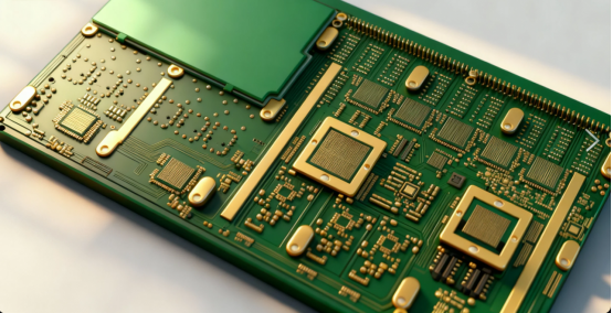
Gold fingers are the connecting components used between printed circuit boards, enabling circuit connection and signal transmission. The nickel-gold layer on the gold finger surface consists of a nickel layer as an intermediate layer, onto which gold is plated. During the gold plating process, multiple layers are deposited to enhance durability and conductivity. This structure not only improves durability against repeated insertions, electrical conductivity, and oxidation resistance in these areas, but also provides a solderable surface for reliable component attachment. The gold-plated surface offers good solderability, especially for fine-pitch components.
In traditional processes, creating PCB gold fingers required adding plating leads to the areas needing nickel-gold plating before design and production, to conduct current during the plating process. After plating, the leads were removed via beveling or milling, but this left plating lead residues at the root of the gold fingers.
In contrast, leadless gold plating technology uses a chemical etching method instead of mechanical processing to form the gold fingers without leads. It simultaneously solves quality issues like copper whiskers and burrs on the gold fingers caused by mechanical processing.
Why is Leadless Gold Plating Technology So Important?
Modern electronic products demand extremely high signal transmission quality, and leadless gold plating technology meets this need precisely. In the manufacturing process of the pcb board, leadless gold plating not only streamlines production by eliminating the need for additional lead wires, but also improves performance and design flexibility. Its main advantages manifest in three key areas:
Enhancing Signal Integrity
In traditional processes involving designs with gold fingers of varying lengths, the lead lengths were unequal. Plating lead residues cause signal interference, severely affecting the electromagnetic compatibility of electronic devices.
The leadless design eliminates the signal reflection and impedance discontinuity problems caused by lead residues, providing a cleaner transmission environment for high-frequency signals.
Improving Reliability and Durability
Leadless PCB gold plating technology employs thick gold plating for the gold fingers. It uses automated current input devices instead of manual current application methods, solving the issue of uneven gold plating on the gold fingers.
This results in gold fingers with superior insertion-durability and oxidation resistance, extending connector lifespan and enhancing the overall reliability of electronic products.
Adapting to Miniaturization Trends
As electronic components shrink in size and PCB assembly density increases, the leadless design frees up the valuable space previously occupied by lead residues. This allows for more compact circuit board layouts, aligning with the thinner, lighter, shorter, smaller evolution of electronic products.
Core Technologies in Leadless PCB Gold Plating
Achieving high-quality leadless PCB gold plating relies on several key process technologies, each critical to the final product quality. In PCB manufacturing, selecting the right surface finish is essential for protecting the copper circuitry, ensuring solderability, and meeting the requirements of various applications. There are several surface finishes available, such as gold plating, immersion gold, and others, each offering unique benefits. For gold plating, there are two methods commonly used: electroless plating and electroplating. These methods are chosen based on the desired properties and application requirements of the PCB.
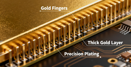
Thick Gold Plating for Gold Fingers
This technology uses automated current input devices instead of manual methods, resolving the issue of uneven gold distribution on gold fingers. During the plating process, gold plates are formed as a thicker layer of gold is applied to the gold fingers for enhanced durability. This results in a robust layer of gold on the contact points, making gold plated gold fingers the standard for high-reliability connectors.
Optimization of dummy gold finger design addresses burning issues caused by instantaneous current contact. Hard gold plating is used for gold fingers to improve wear resistance, as hard gold provides a wear resistant finish ideal for applications requiring repeated insertion and abrasion. Using anti-plating inks instead of secondary masking methods prevents gold seepage (plating bleed) on the fingers.
Triple Masking Alignment Process (±2mil)
By controlling the expansion and contraction of the three dry film negatives and improving the equipment alignment procedures, the pattern transfer alignment capability is enhanced, ensuring it meets the stringent ±2mil requirement.
This process demands extreme precision, equivalent to tolerances within one-tenth the diameter of a human hair.
Chemical Etching Replaces Mechanical Processing
Leadless PCB gold plating uses chemical etching methods instead of mechanical machining to form the leadless gold fingers, solving quality problems like copper whiskers and burrs caused by mechanical processing.
The chemical etching process enables more precise edge control and avoids the effects of mechanical stress on the board substrate.
In addition to chemical etching, various alternative surface finishes are used in PCB manufacturing, such as tin, immersion tin, immersion gold, immersion gold ENIG, electroless nickel immersion gold, immersion silver, and silver. Immersion finishes like immersion gold and immersion gold ENIG deposit a thin layer of gold, resulting in a flat and even surface that is especially beneficial for fine pitch components requiring reliable, uniform solder joints. These finishes provide a flatter surface compared to traditional plating, improving solderability and overall product quality. Immersion tin and immersion silver are lead free, making them suitable for environmentally conscious and RoHS-compliant applications. The thin layer of metal deposited by these processes enhances solderability and can extend the shelf life of the PCB finish. During soldering, the gold dissolves into the solder, which improves electrical connectivity. Gold immersion is a process specifically used for certain PCB finishes to achieve these benefits. Other metals, such as nickel, cobalt, and various alloys, are also used in surface finishes, with each metal affecting the performance, durability, and conductivity of the PCB in different ways.
Leadless vs. Traditional Gold Plating: A Comparison
Leadless gold plating differs fundamentally from traditional processes, impacting PCB performance and reliability.
·Application Scope
Traditional gold plating is typically applied to specific areas of the PCB, such as gold fingers or contact pads, rather than the entire pcb. This targeted approach is used to enhance durability and contact quality in locations that experience frequent connection and disconnection.
·Performance Comparison
Leadless gold plating offers superior corrosion resistance and excellent solderability, making it ideal for high-reliability and harsh-environment applications. It also provides high conductivity, ensuring reliable signal transmission across critical connections. These properties are essential for maintaining performance and durability in demanding conditions.
·Reliability in Use
Gold-plated connectors are highly reliable when interfacing with other electronic components, especially in assemblies where repeated connections and disconnections occur. This reliability is crucial for maintaining consistent electrical performance and mechanical stability.
Process Flow Differences
Traditional gold plating requires adding plating leads, which are removed by mechanical processing after plating, unable to fully eliminate lead residue.
The modern leadless process uses chemical etching methods combined with triple pattern transfer technology to achieve a completely leadless gold finger structure.
Performance Comparison
Gold fingers produced by traditional methods carry the risk of signal interference, and mechanical processing can lead to quality issues like copper whiskers and burrs.
Leadless gold plating technology provides a cleaner signal transmission environment, excellent gold surface uniformity, and better solder mask adhesion.
Cost-Benefit Analysis
Although the leadless gold plating process increases procedural complexity, it reduces product rework and failure rates caused by signal issues. From a total lifecycle perspective, it offers a higher return on value.
Especially for high-performance electronic products, preventing product failures due to signal integrity issues yields far greater benefits than the increased process costs.
Application Scenarios for Leadless PCB Gold Plating
Due to its superior performance, leadless PCB gold plating technology is already widely used in several high-end fields.
Communication Equipment
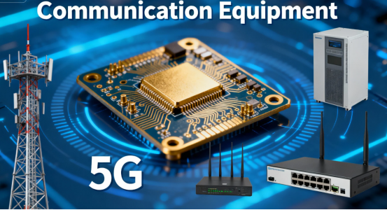
As the communications sector evolves, the operating environments for optical module products are becoming increasingly complex, demanding higher performance from PCB gold fingers.
Leadless gold plating meets the stringent signal integrity requirements of high-speed optical communication modules, making it the preferred process for 5G/6G communication equipment.
High-Performance Computing

In areas like servers and supercomputers, signal transmission speed and stability are paramount. Leadless gold-plated PCBs ensure high-speed signal transmission quality, meeting the extreme reliability demands of data centers.
Automotive Electronics

Automotive electronic systems, particularly Advanced Driver Assistance Systems (ADAS), have exceptionally high requirements for the reliability and durability of electronic components. The connection stability provided by leadless gold plating makes it an ideal choice for safety-critical automotive systems.
Industrial Control
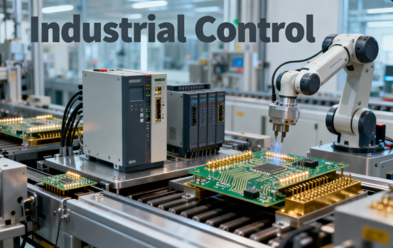
Electronic equipment in industrial environments often faces challenges like vibration and temperature fluctuations. The high-reliability contact provided by leadless gold-plated connectors ensures the stable operation of industrial control systems in harsh conditions.
Technical Challenges and Solutions in Leadless Gold Plating
Implementing leadless PCB gold plating faces several technical challenges, for which the industry has developed corresponding solutions.
Controlling Plating Uniformity
·Challenge: The leadless design causes uneven current distribution, resulting in variations in gold layer thickness.
·Solution: Using automated current input devices instead of manual methods, and optimizing the dummy gold finger design to prevent burning caused by instantaneous current contact.
Alignment Precision Issues
·Challenge: Insufficient alignment accuracy during multiple pattern transfers leads to deviations in plating position.
·Solution: By controlling the expansion/contraction of the three dry film negatives and improving equipment alignment procedures, the pattern transfer alignment capability is enhanced, ensuring it meets the ±2mil requirement.
Plating Bleed (Seepage)
·Challenge: Metal seeps into non-target areas during plating, causing short circuits.
·Solution: Using anti-plating inks instead of secondary masking methods to prevent gold seepage on the fingers.
Solder Mask Adhesion
·Challenge: Poor adhesion between the gold surface and solder mask ink, leading to ink peeling.
·Solution: Employing ultra-roughing pretreatment technology to improve copper surface roughness and optimizing process control parameters, thereby enhancing ink adhesion to the copper surface.
Future Trends in Leadless PCB Gold Plating

Technological progress never stops, and leadless PCB gold plating is also continuously evolving, heading in the following directions:
Further Improvement in Process Precision
As the frequency of electronic devices keeps increasing, the precision requirements for leadless gold plating will become even stricter. The ±2mil alignment tolerance will be further reduced, driving advances in micro-fabrication technology.
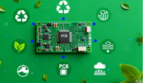
Development Towards Green and Eco-Friendly
The electronics manufacturing industry faces growing environmental demands. Leadless gold plating technology will evolve towards cyanide-free gold plating and reduced chemical consumption, minimizing environmental impact.
Integration with New Surface Treatment Processes
Leadless gold plating will be combined with surface treatment processes like OSP (Organic Solderability Preservative), enabling mixed processes where specific circuit areas, key pads, or solder pads require gold plating while other areas undergo OSP treatment on the same board.
Adaptation to Higher Density Assembly
With the development of chip packaging technology, the assembly density on PCBs will continue to increase. Leadless gold plating technology will adapt to this trend, supporting the assembly of higher density components.
Summary
Leadless PCB gold plating technology has transitioned from a specialized requirement to a standard feature in high-end electronic products. With the rapid development of 5G, IoT, AI, and other technologies, the demands on signal transmission quality will only intensify, making the role of leadless PCB gold plating increasingly critical.
From smartphones to high-speed servers, from automotive electronics to industrial control, this technology quietly underpins the reliable operation of modern electronic devices. As one expert noted, "In the realm of precision electronics, the most successful technologies are often the unnoticed ones—they just work silently, never failing."
Leadless PCB gold plating is precisely such a technology: it doesn't seek attention but strives for reliability; it doesn't stand out but remains indispensable.
FAQs
Q. What is leadless PCB gold plating?
A. It is a process that deposits a gold layer on the surface of pads for leadless PCBs (such as QFN, LGA), aimed at enhancing soldering reliability and oxidation resistance.
Q. Why does a leadless PCB require gold plating?
A. Leadless components rely on direct soldering to pads. Gold plating prevents pad oxidation, ensures solder wettability during soldering, and avoids cold soldering (especially suitable for fine-pitch leads).
Q. What are the common gold plating processes?
A. Mainly electroless gold plating (ENIG) and electroplating: ENIG provides uniform plating, suitable for precision pads; electroplating offers controllable thickness but is costlier, mostly used in high-reliability scenarios.
Q. What are the requirements for gold plating thickness?
A. Typically 0.05–0.2μm (thin gold), balancing cost and solderability; for high-reliability scenarios (e.g., military applications), it can be increased to 0.5μm or more.
Q. Can excessive gold plating thickness cause issues?
A. Yes. Excessive thickness may lead to "gold embrittlement" (high gold content in solder joints causing increased brittleness), reducing connection strength. It is recommended to control it within specifications.
Q. Compared to leaded PCB gold plating, what special requirements does leadless PCB have?
A. It requires higher plating uniformity (due to small pad spacing on leadless PCBs), and gold accumulation at pad edges must be avoided to prevent soldering positioning issues.
What inspections are required after gold plating? Inspections include plating thickness, uniformity, adhesion (tape test), and solder wettability (verified through simulated reflow soldering).
Author: Jack Wang

