Copper Clad Printed Circuit Boards vs. Standard PCBs: What’s the Difference?
In the world of modern electronics, every millimeter of copper counts. As devices become faster, smaller, and more power-dense, engineers face a critical design question: Should you rely on a standard PCB, or upgrade to a copper clad printed circuit board (CCPCB)?
This isn’t just a matter of materials—it’s a choice that defines how efficiently your circuits manage heat, handle signal integrity, and maintain long-term reliability. Copper clad PCBs are reshaping high-performance electronics, from automotive systems to RF modules, pushing the boundaries of what conventional boards can deliver.
Before diving into materials, layers, and performance data, it’s worth asking: What truly sets copper clad boards apart—and when do they make the difference between a good design and a great one?
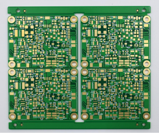
Introduction to Copper Clad and Standard PCBs
What Are Printed Circuit Boards (PCBs)?
A Printed Circuit Board (PCB) is the foundation of almost every electronic device, providing both mechanical support and electrical connections between components. Instead of using bulky wires, PCBs use thin copper traces etched onto a non-conductive base to connect resistors, capacitors, chips, and other parts in a compact layout.
Standard PCBs are typically made using FR-4 (fiberglass epoxy), CEM-1 (composite epoxy material), or polyimide as the base substrate. These materials are chosen for their insulation strength, heat resistance, and cost-effectiveness.
For example:
FR-4 is the industry standard for most consumer and industrial electronics.
CEM-1 is used in simpler single-layer PCBs, such as household appliances.
Polyimide is preferred in flexible or high-temperature applications like aerospace circuits.
In short, a PCB acts as the backbone of electronic systems, determining how signals travel and how reliably a device performs over time.
Overview of Copper Clad Printed Circuit Boards (CCPCBs)
A Copper Clad Printed Circuit Board (CCPCB) begins with a copper clad laminate—a dielectric substrate sheet that has been laminated with one or more thin copper foil layers. This copper layer is later etched to form the circuit pathways that carry current between components.
The structure is simple yet powerful:
Base material (such as FR-4, metal, or ceramic) provides insulation and mechanical strength.
Copper foil acts as the conductive surface for creating circuit traces.
Copper clad boards are the starting material for nearly all types of PCBs—whether single-sided, double-sided, or multilayer designs. Because of the direct bonding between the copper foil and the substrate, these boards ensure excellent adhesion, conductivity, and thermal stability.
For instance, in high-frequency or power electronic devices, thicker copper cladding allows better current carrying capacity and heat dissipation, improving overall performance.
Why This Comparison Matters
Choosing between copper clad PCBs and standard PCBs is not just a technical decision—it’s a strategic one. The type of PCB material and copper structure directly influences:
Thermal performance: Copper clad boards handle heat more efficiently, making them ideal for LED lighting and automotive systems.
Electrical performance: They provide lower signal loss and better impedance control for high-speed or RF circuits.
Cost and manufacturing complexity: Standard FR-4 boards are more economical for mass-produced consumer devices, while copper clad variants are used where performance and durability outweigh cost.
In practical terms:
Standard PCBs dominate in smartphones, laptops, and IoT devices.
Copper clad PCBs excel in power converters, communication base stations, and radar systems.
Understanding the core differences between these two board types helps engineers make informed decisions that balance budget, reliability, and performance requirements—setting the stage for innovation in modern electronics.
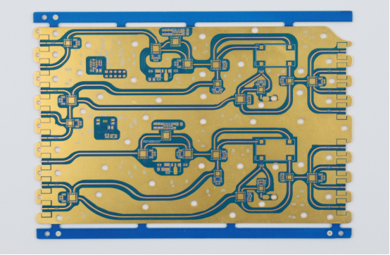
Structural Differences Between Copper Clad and Standard PCBs
Understanding the structural differences between copper clad and standard PCBs is key to optimizing performance and reliability. Differences in layer composition, copper integration, and manufacturing directly affect thermal management, current capacity, and design complexity, helping engineers make informed material and design choices.
Material Composition
The material composition is the most fundamental difference between a copper clad printed circuit board (CCPCB) and a standard PCB.
A copper clad PCB uses a base substrate laminated with a sheet of copper foil. Common base materials include:
FR-4 glass epoxy – widely used for general-purpose boards, offering good insulation and mechanical strength.
CEM-3 – a smoother, white alternative to FR-4, used in lower-cost applications.
Aluminum or metal-core substrates – chosen for high-power or LED applications where thermal conductivity is critical.
By contrast, standard PCBs may use similar substrates but are built from multiple prepreg layers, with copper applied and etched during each lamination cycle rather than starting from a pre-laminated sheet.
Another key distinction lies in the dielectric layer and copper foil thickness.
Copper clad laminates typically come in standard copper weights such as 1 oz (35 μm), 2 oz (70 μm), or even 3 oz (105 μm) for high-current circuits.
The resin system in CCPCBs—such as epoxy or polyimide—determines the board’s dielectric constant, flexibility, and temperature resistance.
In simple terms:
Copper clad PCBs use a single integrated copper layer bonded to the substrate, while standard PCBs build up their copper and dielectric layers step by step during manufacturing.
Layer Construction
Structurally, a copper clad PCB is straightforward. It consists of:
1. Base substrate – provides mechanical support and electrical insulation.
2. Copper foil layer – bonded tightly to one or both sides of the substrate.
3. Etched circuit pattern – formed by removing unwanted copper to create the conductive traces.
This simple structure is ideal for single- or double-sided PCBs, which are common in power supplies, lighting modules, and RF devices.
In contrast, a standard multilayer PCB includes several complex elements:
Signal layers: multiple copper layers separated by dielectric prepregs.
Vias and through-holes: drilled and plated to connect layers vertically.
Prepreg and core layers: bonded under heat and pressure during lamination.
Because of this complexity, standard PCBs can support dense circuit routing, high-speed signals, and compact multilayer stacking, while copper clad boards focus on strength, thermal stability, and high current capacity.
Key takeaway: Copper clad PCBs are typically single-structure boards, whereas standard PCBs are multi-layer composites designed for more complex circuitry.
Manufacturing Process
The manufacturing process for copper clad PCBs and standard PCBs diverges significantly.
1. Copper Clad PCB Production:
Starts with copper clad laminate (CCL), where a dielectric substrate is bonded to copper foil under high temperature and pressure.
The board is then cut, cleaned, coated with photoresist, and etched to define the desired circuit pattern.
Finally, holes are drilled, and the surface is treated or plated for solderability.
2. Standard PCB Fabrication:
Involves multiple lamination cycles to stack copper and dielectric layers.
Includes plating processes to form interconnections between layers (vias and through-holes).
Requires precise layer alignment and registration to maintain signal integrity across layers.
Because copper clad boards begin with pre-bonded copper foil, they offer better copper adhesion and dimensional stability. However, this also means tighter design tolerances are required during etching and drilling, especially for fine-pitch or high-density designs.
For example:
In a 1 oz copper clad board, a slight over-etch can remove significant trace width, affecting performance.
In multilayer standard PCBs, design tolerances are distributed across layers, allowing for more flexibility in adjustment during manufacturing.
In summary: Copper clad PCBs emphasize simplicity and thermal reliability, while standard PCBs prioritize flexibility and interconnect complexity through advanced lamination and plating processes.
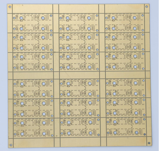
Performance Comparison
When evaluating copper clad printed circuit boards (CCPCBs) against standard PCBs, performance differences become clear in areas like thermal management, electrical behavior, mechanical stability, and environmental durability. These factors determine how well a circuit performs under real-world operating conditions.
Thermal Conductivity
Copper clad PCBs have significantly better thermal conductivity than standard FR-4-based PCBs. Copper’s thermal conductivity is around 400 W/m·K, while FR-4 materials typically range between 0.25–0.3 W/m·K—a difference of more than a thousandfold.
This means copper clad boards can dissipate heat quickly, preventing temperature buildup that can damage sensitive components. In LED lighting modules or power converters, for example, copper clad boards help maintain uniform temperatures across the board, extending component lifespan and ensuring consistent brightness or power efficiency.
Key takeaway: Copper clad PCBs excel in high-power or thermally demanding applications because copper conducts heat away far more efficiently than the resin-based FR-4 used in standard boards.
Electrical Performance
In electronic design, electrical performance depends heavily on how signals move through the board. Copper clad PCBs provide lower signal loss, better impedance control, and superior high-frequency stability compared to standard boards.
This performance advantage comes from both the purity of the copper layer and the low-loss dielectric materials used in high-end copper clad laminates. For example:
Standard FR-4 materials have a dielectric constant (Dk) around 4.3–4.7 and a dissipation factor (Df) of 0.02–0.025 at 10 GHz.
Advanced copper clad laminates (such as IT-968G or Rogers 4350B) feature Dk ≈ 3.2–3.5 and Df ≤ 0.005, minimizing energy loss and distortion in high-speed circuits.
As a result, copper clad PCBs are the preferred choice in RF modules, radar systems, high-speed routers, and 5G base stations, where even small impedance mismatches can degrade signal integrity.
In short: Copper clad PCBs support faster, cleaner signal transmission—critical for modern high-frequency and data-intensive electronics.
Mechanical Strength and Durability
Mechanically, standard PCBs made with FR-4 or CEM-3 offer good rigidity but may warp or delaminate under continuous thermal cycling. Copper clad PCBs, on the other hand, provide enhanced mechanical strength due to the strong copper-substrate bond.
Flexural strength: Copper clad laminates are less prone to cracking or bending under stress.
Moisture resistance: The dense copper layer reduces moisture absorption, preventing expansion or layer separation.
Warping tendencies: Copper distributes heat evenly, lowering the risk of thermal deformation in high-power circuits.
This combination of strength and dimensional stability makes copper clad PCBs ideal for automotive electronics, industrial control boards, and aerospace modules, where vibration and temperature fluctuations are common.
Summary point: Copper clad boards maintain structural integrity and reliability even under mechanical or thermal stress, outperforming standard FR-4 designs.
Environmental and Reliability Factors
Environmental stability is another key differentiator. Copper clad PCBs are designed for long-term reliability in harsh operating conditions.
Oxidation resistance: Protective surface treatments (such as ENIG or OSP) prevent copper oxidation, ensuring consistent conductivity.
Temperature cycling: Copper’s high thermal stability allows boards to endure rapid temperature changes without cracking or delaminating.
Aging and stability: The tight bonding between copper and the dielectric substrate reduces the risk of performance drift over years of use.
Standard PCBs, while cost-effective, may suffer degradation in extreme humidity, temperature, or high-current environments. Copper clad boards maintain electrical and mechanical consistency, even after prolonged exposure to challenging conditions.
Key insight: For industries where durability and long-term reliability are non-negotiable—such as defense, automotive, or telecommunications—copper clad PCBs deliver superior environmental endurance.
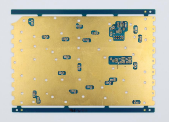
Application Scenarios
Different industries rely on Copper Clad Printed Circuit Boards (CCPCBs) and standard PCBs to meet specific design and performance requirements. The choice depends on factors like power density, frequency range, cost targets, and environmental conditions.
Typical Uses of Copper Clad PCBs
Copper clad PCBs are engineered for applications that demand high thermal conductivity, strong current capacity, and low signal loss. Their robust copper layers and stable dielectric substrates make them ideal for high-performance and high-power electronics.
Common applications include:
Power electronics: 2-layer or metal-core copper clad boards are used in power converters, inverters, and motor drivers to manage large current loads efficiently.
RF and microwave circuits: In devices like radar systems, satellite communication modules, and 5G base stations, copper clad laminates ensure minimal signal loss and precise impedance control.
LED lighting modules: The high thermal conductivity of copper clad substrates helps dissipate heat and extend LED lifespan, ensuring consistent brightness and color stability.
Automotive electronics: Copper clad PCBs are found in ECUs (Electronic Control Units), battery management systems (BMS), and onboard chargers, where reliability under vibration and temperature stress is essential.
Real-world example:
A 2-layer copper clad PCB used in an industrial power converter can carry several amperes of current per trace, outperforming standard FR-4 boards while keeping temperatures within safe limits.
In summary: Copper clad PCBs dominate applications where heat management, current capacity, and frequency precision are critical to performance.
Typical Uses of Standard PCBs
Standard PCBs remain the backbone of consumer and commercial electronics, offering a cost-effective balance of performance and manufacturability. These boards are optimized for compact, multi-layer circuitry and are compatible with automated assembly processes.
Common applications include:
Consumer electronics: Used in smartphones, laptops, tablets, and wearables, where multi-layer FR-4 PCBs enable dense circuit routing and high-speed signal transmission.
Computers and servers: Multilayer standard PCBs form the backbone of motherboards, GPUs, and storage controllers, integrating high-speed data and power lines.
Telecommunications equipment: Found in routers, IoT modules, and baseband processors, where reliability and low cost are key design drivers.
Example:
A 6-layer standard FR-4 PCB in a smartphone motherboard manages high-speed data lines for the processor, memory, and wireless chipsets—all within a thin, lightweight structure.
In short: Standard PCBs provide excellent design flexibility and cost efficiency for mass-produced electronic systems.
How to Choose Between the Two
Selecting the right PCB type depends on performance requirements, cost targets, and operating environment. Engineers should evaluate each factor before finalizing materials and stack-up configurations.
Step-by-step decision framework:
1. Define power and thermal needs – Choose copper clad PCBs for high-current or heat-sensitive circuits.
2. Assess frequency and signal integrity – For RF or high-speed designs, low-Df copper clad laminates perform better.
3. Evaluate cost and production scale – Standard FR-4 PCBs are more economical for high-volume manufacturing.
4. Consider environmental factors – Copper clad PCBs excel in harsh, high-temperature, or vibration-prone conditions.
Comparison Table: Copper Clad PCBs vs. Standard PCBs
Parameter
Copper Clad PCB
Standard PCB (FR-4, CEM-1)
Thermal Conductivity
Very High (up to 400 W/m·K) Low (0.25–0.3 W/m·K)
Electrical Performance
Low Dk/Df, stable at high frequencies
Moderate Dk/Df, limited for high-speed use
Current Carrying Capacity
Excellent, supports heavy loads
Moderate, suitable for small currents
Mechanical Strength
Strong copper adhesion, low warpage
Good rigidity, may warp under heat
Cost Level
Higher
Lower
Typical Use Cases
Power converters, RF, LED, automotive
Consumer electronics, computing, IoT
Parameter
Copper Clad PCB
Standard PCB (FR-4, CEM-1)
Thermal Conductivity
Low (0.25–0.3 W/m·K)
Electrical Performance
Low Dk/Df, stable at high frequencies
Moderate Dk/Df, limited for high-speed use
Current Carrying Capacity
Excellent, supports heavy loads
Moderate, suitable for small currents
Mechanical Strength
Strong copper adhesion, low warpage
Good rigidity, may warp under heat
Cost Level
Higher
Lower
Typical Use Cases
Power converters, RF, LED, automotive
Consumer electronics, computing, IoT
Key takeaway:
Choose copper clad PCBs for performance-critical or thermally demanding applications, and standard PCBs for cost-sensitive, compact, or high-volume products.
Cost and Manufacturing Considerations
The choice between Copper Clad Printed Circuit Boards (CCPCBs) and standard PCBs often comes down to more than just performance—it’s also about cost, process complexity, and scalability. Understanding these economic and production factors helps engineers and procurement teams make informed design decisions.
Material Cost Analysis
The material composition of a PCB has a direct impact on overall cost.
Copper clad PCBs use higher-grade copper foil and specialized laminates, which are more expensive than those used in standard PCBs. The cost components typically include:
Copper foil: High-purity copper (1 oz to 3 oz) adds both cost and performance value. Thicker copper layers improve current capacity but increase raw material expense.
Laminate materials: Advanced laminates such as metal-core, ceramic-filled, or low-loss materials (e.g., IT-968G, Rogers 4350B) cost more than standard FR-4 or CEM-1 substrates.
Processing costs: Etching thicker copper layers requires more chemicals, precise control, and extended process times, further increasing production cost.
By comparison, standard PCBs—using FR-4 or CEM-based materials—offer a more cost-efficient balance between performance and manufacturability. These materials are widely available, easy to process, and well-suited for high-volume, low-cost production.
Key insight: Copper clad PCBs have higher material and processing costs due to thicker copper foils and advanced laminates, while standard PCBs benefit from low-cost, mass-available materials.
Production Complexity
From a manufacturing standpoint, copper clad PCBs require greater precision and tighter process control.
Etching precision: Because of thicker copper layers, achieving accurate trace widths and spacing is more difficult. Over-etching can distort circuits, especially in fine-line designs.
Inspection and quality control: Copper clad boards demand more rigorous inspection for surface flatness, adhesion quality, and copper uniformity.
Tool wear and process time: Drilling through thicker copper or metal substrates causes more tool wear and longer cycle times, slightly reducing yield rates.
In contrast, standard PCBs are easier to fabricate using automated etching, plating, and lamination techniques. With mature production lines and optimized yield rates above 98%, FR-4-based PCBs are the most efficient choice for consumer electronics and large-scale manufacturing.
Summary statement: Copper clad PCBs require more complex etching and inspection processes, while standard PCBs offer simpler, faster, and higher-yield manufacturing workflows.
Scalability for Mass Production
When scaling up production, factors such as material supply, standardization, and manufacturing infrastructure become critical.
Scalability depends on both material availability and process flexibility:
Supply chain stability: FR-4 and CEM materials are globally standardized, available in consistent quality and large volumes. Copper clad laminates, especially those with metal cores or advanced resins, may require specialized suppliers and longer lead times.
Standard panel sizes: Standard PCBs use commonly available panel dimensions (18×24 or 21×24 inches), optimizing material utilization. Copper clad materials—particularly aluminum- or ceramic-based boards—may need custom cutting and handling, increasing waste and cost.
Automation readiness: Standard PCB production is easily automated for SMT (Surface Mount Technology) lines, while copper clad boards often require manual or semi-automated processes due to their thickness and rigidity.
However, when produced at scale, optimized fabrication systems can significantly reduce per-unit cost even for copper clad PCBs, balancing performance with economic efficiency.
Key takeaway: Standard PCBs are inherently more scalable for mass production, while copper clad PCBs, though more costly to produce, can be efficiently manufactured in moderate-to-high volumes with advanced process control.
Future Trends and Innovations
The printed circuit board (PCB) industry continues to evolve rapidly, driven by demands for higher speed, better thermal management, and sustainability. In particular, copper clad printed circuit boards (CCPCBs) are at the forefront of this innovation wave, with advancements in materials, hybrid architectures, and eco-friendly manufacturing shaping the future of electronics design.
Advancements in Copper Clad Laminate Technology
The next generation of copper clad laminates (CCLs) is redefining how PCBs handle heat, frequency, and reliability. Modern developments focus on materials that deliver low dielectric loss, high thermal stability, and environmental safety.
Low-loss and high-Tg materials such as IT-968G and Rogers 4000/6000 series are leading examples. These laminates offer:
Dielectric loss (Df) values below 0.005 @10 GHz, enabling excellent signal integrity for high-frequency designs.
High glass transition temperature (Tg), improving performance under extreme thermal cycling.
Halogen-free formulations, reducing environmental impact and aligning with global RoHS and REACH regulations.
These advanced laminates are increasingly used in 5G base stations, radar systems, power converters, and EV control units, where stability and low signal loss are critical.
Key statement: Future copper clad laminates will prioritize low-loss, high-Tg, and halogen-free properties to meet the growing performance and sustainability demands of modern electronics.
Hybrid PCB Designs
A significant trend in next-generation electronics is the rise of hybrid PCB architectures, which combine copper clad layers with standard FR-4 or multilayer PCBs. This approach allows engineers to balance cost, performance, and mechanical flexibility within the same board.
In a hybrid PCB, critical high-power or high-frequency zones—such as RF amplifiers or power regulators—are built using metal-based copper clad layers for superior heat dissipation. Meanwhile, low-speed digital control sections are fabricated on conventional FR-4 for cost efficiency and easier routing.
For example:
An automotive power management unit may use a 2-layer copper clad section for power transistors and a 6-layer FR-4 section for signal control.
In telecom modules, hybrid boards integrate Rogers high-frequency layers with standard prepregs for precise impedance control and reduced insertion loss.
Key insight: Hybrid PCB designs offer a practical solution for engineers who need the thermal and electrical advantages of copper clad boards without the full material cost of all-metal structures.
Sustainability and Recycling
As global electronics production scales, sustainability has become a defining factor in PCB innovation. Traditional PCB manufacturing generates significant material waste, especially from copper etching and laminate cutting. The next generation of copper clad PCBs focuses on recycling and eco-friendly substrates to reduce this footprint.
Emerging practices include:
Copper recovery systems, where etching solutions are filtered and reused to reclaim pure copper.
Eco-laminates made from bio-based resins or halogen-free composites, reducing toxic byproducts.
Closed-loop recycling, allowing copper layers and dielectric materials to be separated and reprocessed.
In addition, manufacturers are adopting green fabrication technologies—including water-based cleaning, reduced VOC emissions, and optimized panel utilization—to minimize environmental impact without compromising quality.
Summary statement: The future of copper clad PCB manufacturing will emphasize recyclability, eco-friendly materials, and closed-loop production systems to achieve both performance and sustainability goals.
Final Outlook
As electronics continue to push the boundaries of speed, power, and miniaturization, the synergy between advanced copper clad materials, hybrid designs, and sustainable practices will define the next decade of PCB innovation. Companies are already investing in these frontiers—bridging high performance with responsible engineering.
Conclusion
When comparing copper clad PCBs with standard PCBs, several key differences stand out that directly affect performance, cost, and design decisions. Copper clad boards excel in thermal management, quickly dissipating heat in high-power devices, LED modules, and automotive electronics. They also provide superior electrical stability, with low signal loss and precise impedance control, making them ideal for high-frequency or RF applications. Mechanically, copper clad PCBs are more resistant to warping, vibration, and thermal cycling, ensuring long-term durability in demanding environments.
In contrast, standard FR-4 or CEM-based PCBs offer a cost-effective and scalable solution for mass-produced consumer electronics, computers, IoT devices, and other low-to-moderate power applications. They provide sufficient electrical performance and mechanical strength for everyday electronic products, while keeping production costs low and manufacturing workflows simple.
Choosing the right PCB type depends on project requirements. Copper clad PCBs are the best choice when performance, reliability, and thermal management are critical, while standard PCBs are suitable for applications where cost efficiency and scalability are the main priorities. Leveraging advanced materials and precise manufacturing processes, PCBMASTER delivers both high-performance copper clad boards and optimized standard PCBs, helping engineers select the ideal solution for each project and ensuring designs achieve maximum reliability, efficiency, and long-term stability.
FAQs
What is the main advantage of using a copper clad PCB over a standard PCB?
The main advantage of a copper clad PCB is its superior thermal and electrical performance. The copper layer enables better heat dissipation, lower signal loss, and precise impedance control, making it ideal for high-power, high-frequency, or RF applications, where standard FR-4 or CEM-based PCBs may not perform adequately.
Can copper clad PCBs handle higher temperatures?
Yes. Copper clad PCBs can handle higher temperatures than standard PCBs. The copper layer efficiently distributes heat across the board, and advanced laminates with high glass transition temperature (Tg) provide thermal stability, reducing warping and improving reliability in power electronics, automotive, and industrial applications.
Are copper clad PCBs more expensive to produce?
Yes. Copper clad PCBs generally have higher material and manufacturing costs. This is due to thicker copper foils, advanced laminates, and more precise etching and inspection processes. Standard FR-4 PCBs remain more cost-effective for low-to-moderate power, mass-produced consumer electronics.
What types of copper clad materials are commonly used in high-frequency applications?
High-frequency applications typically use low-loss, high-Tg copper clad laminates such as:
IT-968G – optimized for minimal dielectric loss and thermal stability.
Rogers laminates (e.g., 4350B, 4000 series) – provide low dissipation factor (Df ≤ 0.005) and stable dielectric constant (Dk ≈ 3.2–3.5) for RF and microwave circuits.
How does copper thickness affect PCB performance?
Copper thickness directly influences current carrying capacity, thermal dissipation, and mechanical strength:
Thicker copper (e.g., 2–3 oz per square foot) allows higher currents without overheating, reduces trace resistance, and improves heat spreading.
Thinner copper (e.g., 1 oz) is suitable for lower-power or high-density boards but has lower current capacity and thermal performance.
Copper thickness also affects etching precision and design tolerances, especially in fine-line or high-density circuits.


