


PCB Silkscreen Printing: Materials, Methods & Troubleshooting Guide
Printed circuit boards (PCBs) form the foundation of modern electronic devices, where every detail—from layout to markings—can impact performance and reliability. Among these details, silkscreen printing is essential: it guides component placement, enhances readability, and gives your PCB a polished, professional look.
Whether you’re an engineer, designer, or electronics hobbyist, mastering the materials, printing methods, and troubleshooting techniques for PCB silkscreen can save time, reduce errors, and ensure high-quality results. This guide walks you through everything you need to know to achieve precise, durable, and visually clear silkscreen printing for your next PCB project.
Introduction to PCB Silkscreen Printing
What is PCB Silkscreen Printing?
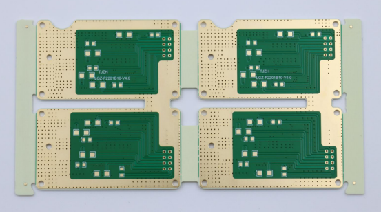
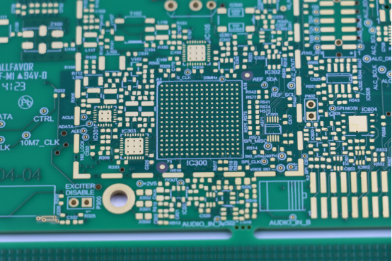
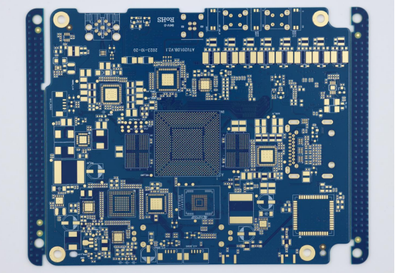
PCB silkscreen printing is the process of applying labels, symbols, and text onto a PCB using specialized ink. These markings help engineers and assembly teams identify components, orientation, test points, and other critical information.
A key point to understand is the difference between silkscreen and solder mask. While the solder mask is a protective layer that prevents solder bridges and protects copper traces, the silkscreen is purely for labeling and visual guidance. It does not provide electrical insulation or protection.
Silkscreen printing is widely used in various stages of PCB manufacturing. For example:
On a consumer electronics PCB, silkscreen labels indicate resistor and capacitor values for assembly.
In industrial electronics, test points and component orientation markings are printed for easier troubleshooting.
Branding logos or part numbers are often added via silkscreen for identification and traceability.
By clearly marking components and reference points, silkscreen printing ensures smoother assembly and maintenance.
Benefits of Silkscreen Printing
Silkscreen printing offers multiple advantages for both PCB manufacturers and end-users:
Enhances Component Placement and Identification
Labels, polarity marks, and outlines make it easier to place components accurately during assembly. For example, a diode marked with a clear polarity symbol reduces the risk of incorrect installation and ensures the PCB functions as intended.
Improves Assembly Accuracy and Reduces Errors
Clear silkscreen markings help minimize misplacement, soldering mistakes, and inspection failures. Automated assembly machines also rely on these markings to verify component orientation, further improving production efficiency and reducing errors.
Aesthetic and Branding Benefits
Printed logos, part numbers, and labels give the PCB a professional and finished appearance. Additionally, silkscreen markings can help distinguish different revisions of a PCB at a glance, supporting both organization and traceability.
Common Misconceptions
Despite its importance, PCB silkscreen printing is often misunderstood.
Silkscreen is Not a Solder Mask Substitute
Some may assume that silkscreen protects the PCB electrically, but its function is purely visual. It provides guidance for component placement and identification, but for insulation and protection of copper traces, the solder mask layer is required.
Traditional vs. Modern PCB Marking
Traditional silkscreen printing relied on manual screen printing techniques, which could be slower and less precise. Modern methods include automated screen printers, inkjet printing, and laser marking.
For example, inkjet silkscreen allows high-precision markings on dense or complex boards, whereas manual methods are more prone to misalignment and inconsistencies.
Understanding these basics helps manufacturers and designers choose the right methods and materials for their PCB projects.
Materials Used in PCB Silkscreen Printing
Ink Types
PCB silkscreen printing relies on specialized inks to ensure clear, durable, and heat-resistant markings. Two common types of ink are epoxy-based and UV-curable.
Epoxy-based ink is known for its excellent adhesion to the PCB surface and strong durability. It can withstand high-temperature soldering processes without smudging or fading. This makes it suitable for both single-layer and multilayer PCBs in industrial applications.
UV-curable ink dries quickly when exposed to ultraviolet light, enabling faster production cycles. It is particularly suitable for high-volume PCB manufacturing where speed is critical.
When comparing these inks, epoxy-based ink generally offers superior heat resistance and long-term durability, but it may require longer curing times. UV-curable inks are faster and environmentally friendlier, but they may be less resistant to extreme heat. The choice depends on your production requirements, PCB type, and desired print longevity.
PCB Substrate Considerations
The type of PCB substrate directly affects how well silkscreen ink adheres. Common substrates include FR4, Rogers, and flexible PCBs.
FR4 is the most widely used substrate, offering a smooth surface for consistent ink adhesion.
Rogers materials, often used for high-frequency applications, may require specific ink formulations due to their unique surface properties.
Flexible PCBs present challenges such as surface elasticity, which can affect ink durability during bending or flexing.
Surface finishes also impact silkscreen quality. For example:
HASL (Hot Air Solder Leveling) surfaces may create uneven areas, requiring careful ink application.
ENIG (Electroless Nickel Immersion Gold) provides a smooth, flat surface ideal for precise markings.
OSP (Organic Solderability Preservative) coatings can slightly alter ink adhesion and require ink compatibility checks.
Understanding substrate type and surface finish is crucial for achieving consistent, long-lasting silkscreen results.
Consumables and Equipment
High-quality silkscreen printing also depends on proper consumables and equipment.
Screens: The mesh type, tension, and material of the screen influence ink transfer and print clarity. Finer mesh screens enable detailed markings, while coarser meshes are suited for larger graphics.
Squeegees: Hardness and angle selection affect ink deposition. A softer squeegee can conform to uneven surfaces, while a harder one ensures consistent thickness for flat PCBs.
Cleaning Materials and Solvents: Proper cleaning of screens and tools prevents ink contamination and clogging. Using the correct solvents also preserves screen longevity and maintains print quality.
Together, these materials and tools determine the precision, consistency, and durability of silkscreen printing on PCBs.
Silkscreen Printing Methods
Manual Silkscreen Printing
Manual silkscreen printing is a traditional method where a screen and squeegee are used to transfer ink onto the PCB surface. The process typically follows these steps:
Screen Alignment – Position the screen accurately over the PCB to ensure correct placement of markings.
Ink Application – Spread the silkscreen ink evenly across the screen using a squeegee.
Drying – Allow the ink to dry, either at room temperature or using a low-temperature curing process.
Pros and Cons: Manual silkscreen printing is cost-effective and flexible, making it suitable for small production runs or prototype PCBs. However, it can be slower and less consistent compared to automated methods. Human error in alignment or ink application may lead to smudges or uneven prints.
Automated Silkscreen Printing
Automated silkscreen printing uses machines such as stencil printers or automated screen printers to apply silkscreen markings with high precision.
Step-by-step process:
1. PCB Loading – The machine loads PCBs onto the printing platform.
2. Registration – Advanced sensors align the PCB to ensure accurate ink placement.
3. Ink Deposition – The printer applies ink evenly across the stencil or screen.
4. Curing – Ink is cured using heat or UV light for durability.
Comparison to manual printing: Automated methods are faster, more precise, and suitable for high-volume production. They reduce errors and improve repeatability. However, equipment costs are higher, and setup may be less flexible for small batches or custom designs.
Alternative Marking Techniques
Beyond traditional silkscreen, other PCB marking methods include:
Inkjet Printing – Uses precise droplets of ink to print fine details, ideal for dense or high-resolution boards.
Laser Marking – Engraves or ablates markings directly onto the PCB surface, offering permanent and highly accurate labels.
Pad Printing – Transfers ink via a silicone pad, useful for irregular surfaces or curved PCBs.
When to use alternative methods:
Inkjet and laser marking are preferred for high-density or small-footprint PCBs where silkscreen cannot achieve fine detail.
Pad printing is useful for flexible or irregularly shaped PCBs where screens or stencils are impractical.
These alternative methods complement traditional silkscreen printing, allowing manufacturers to select the most suitable technique based on PCB complexity, production volume, and required marking precision.
Design Considerations for PCB Silkscreen
Artwork and Layout Guidelines
When designing PCB silkscreen, clarity and readability are essential. Recommended font types include simple, sans-serif styles, which remain legible at small sizes. The typical font size ranges from 0.8 mm to 1.0 mm for component labels, ensuring text is readable during assembly and inspection.
Line widths and spacing should follow minimum standards to avoid ink bleeding or merging. For most PCBs, a minimum line width of 0.1 mm and a spacing of 0.2 mm between characters or symbols is recommended.
It is also crucial to avoid overlaps with pads or vias, as these areas can interfere with soldering or cause smudging.
For example, resistor outlines should not cross the solder pads, and test point markings should be positioned nearby without touching exposed copper. Following these guidelines ensures precise component placement and reduces assembly errors.
Color Selection
Silkscreen color impacts visibility and contrast. The most commonly used colors are white, black, and yellow. White is the standard choice for dark solder masks like green or blue, while black is often used on light-colored solder masks for better readability. Yellow can be applied for branding or highlighting specific components.
When choosing colors, always consider contrast against the solder mask. High contrast improves legibility, making it easier for assembly operators and automated machines to recognize markings.
For instance, white silkscreen on a green solder mask offers high visibility, whereas yellow on green may be harder to read under certain lighting conditions.
Layering and Masking
PCB silkscreen can be applied on a single side or double-sided. Single-sided silkscreen is sufficient for most standard boards, but double-sided printing is necessary for complex or dense designs where both top and bottom components require labeling.
The solder mask layer plays a key role in preventing ink smearing. By masking exposed copper areas, the solder mask ensures that the silkscreen adheres only to designated areas, maintaining print clarity and durability.
For example, applying silkscreen over masked vias prevents ink from spreading into the holes, which could interfere with component placement or soldering.
Proper layering and masking choices enhance the longevity of the silkscreen and reduce manufacturing defects.
Troubleshooting Common Silkscreen Issues
Misalignment Problems
Misalignment occurs when silkscreen markings are not correctly positioned on the PCB. Common causes include registration errors during manual or automated printing, as well as PCB warping due to uneven heat or substrate stress.
Solutions involve carefully re-aligning the screen or stencil, adjusting fixture clamps, and verifying PCB flatness before printing.
For example, using alignment pins or automated vision systems can reduce registration errors in high-volume production. Correcting misalignment ensures accurate component placement and prevents assembly errors.
Ink Smudging or Smearing
Ink smudging happens when the silkscreen ink spreads beyond intended areas. Key causes include improper curing, applying excessive ink, or surface contamination on the PCB.
Fixes involve adjusting squeegee pressure to ensure even ink deposition, modifying ink viscosity for better flow, and optimizing curing time and temperature.
For instance, reducing squeegee speed can prevent excess ink from smearing across pads. Proper handling during printing and curing maintains clear and precise silkscreen markings.
Missing or Faded Prints
Sometimes silkscreen markings appear incomplete or faint. This issue is often caused by worn screens, poor ink adhesion, or incompatibility with the PCB substrate.
Preventive measures include regularly inspecting and replacing worn screens, selecting inks compatible with the substrate material, and performing test prints before full production. Repair techniques may involve touch-up printing or reprinting affected areas. These steps ensure all component labels remain visible and readable throughout the PCB’s lifecycle.
Environmental and Storage Issues
Environmental factors can significantly impact silkscreen quality. Humidity and temperature fluctuations may cause ink to smear, fade, or fail to cure properly.
Proper storage of both PCBs and screens is essential. Keep PCBs in a controlled, dry environment, and store screens in protective covers to prevent dust accumulation.
For example, storing screens in a low-humidity room preserves mesh tension and prevents ink contamination. Managing environmental conditions ensures consistent print quality across batches.
Quality Control and Testing
Visual Inspection
Visual inspection is a fundamental step in PCB silkscreen quality control. Key criteria include legibility of text and symbols, proper alignment with component pads, and completeness of all markings. Any smudges, missing characters, or overlaps can compromise assembly accuracy.
Tools commonly used for inspection include magnification devices such as microscopes or magnifying lamps, as well as AOI (Automated Optical Inspection) systems. AOI machines can scan the PCB, detect misaligned or missing silkscreen, and flag defects automatically, which is particularly useful in high-volume production. For example, AOI can quickly identify a misprinted resistor label that might be missed in manual inspection.
Functional Testing
Beyond visual checks, functional testing ensures that silkscreen markings do not interfere with PCB performance. Electrical testing can identify shorts or opens that may occur under or near silkscreened areas, especially if ink accidentally covers exposed copper or vias.
Step-by-step, the process typically involves connecting test probes to PCB nets and verifying continuity according to the design schematic. Functional testing guarantees that the PCB operates as intended even after printing.
Standards and Compliance
Adhering to recognized standards ensures consistent quality and manufacturability. The IPC-7351 standard provides guidelines for silkscreen placement, text size, and symbol conventions.
Other relevant standards cover ink adhesion, environmental durability, and inspection protocols.
Compliance with these standards helps manufacturers produce PCBs that meet both industry expectations and customer requirements, while reducing errors during assembly and inspection.
Tips for Optimizing Silkscreen Printing
Process Optimization
Optimizing the silkscreen printing process starts with proper ink mixing, ensuring consistent viscosity and color for even application.
Maintaining correct screen tension is equally important; a screen that is too loose can produce blurry prints, while one that is too tight may damage fine details.
Curing cycles—including temperature, duration, and UV exposure for UV-curable inks—must be carefully controlled to achieve durable, smudge-resistant markings.
For example, adjusting the curing temperature by a few degrees can prevent ink cracking on high-temperature PCBs.
Cost and Time Efficiency
Efficient production requires balancing batch printing versus single PCB printing. Batch printing is ideal for high-volume runs, reducing setup time and material waste, while single PCB printing suits prototypes or small orders.
Another key factor is reducing rework through design foresight. By carefully planning silkscreen layouts, avoiding overlaps with pads or vias, and selecting compatible ink and substrates, manufacturers can minimize errors that would otherwise require additional printing or touch-ups.
For instance, pre-testing layout designs on sample boards can prevent costly mistakes in full production runs.
Maintaining Equipment
Regular maintenance ensures consistent silkscreen quality. Screen cleaning routines remove residual ink and prevent clogging, which maintains clear lines and accurate markings.
Preventive maintenance of printers and squeegees, such as checking mesh tension, replacing worn blades, and calibrating automated machines, prolongs equipment life and reduces downtime.
For example, a regularly cleaned and tensioned screen can maintain print resolution across hundreds of PCBs without noticeable degradation.
Conclusion
High-quality PCB silkscreen printing depends on a combination of careful material selection, optimized printing methods, and effective troubleshooting. By choosing the right inks, considering substrate and surface finishes, and maintaining proper screen and equipment conditions, manufacturers can achieve clear, durable, and accurate markings on every PCB.
Equally important is design foresight. Planning layouts to avoid pad or via overlaps, selecting readable fonts, and applying appropriate color contrast ensures fewer errors and reduces the need for rework. When these practices are combined with precise process control—whether manual or automated—PCB silkscreen results become more reliable, efficient, and professional.
If you have more questions or want to learn more about PCBs, feel free to contact PCBMASTER, an experienced PCB supplier providing expert solutions and professional services to support your projects.
FAQs
1. What is the difference between PCB silkscreen and solder mask?
PCB silkscreen is a layer of ink applied to the PCB surface that contains text, symbols, logos, and component identifiers. Its main purpose is visual guidance for assembly, testing, and troubleshooting. Silkscreen does not provide electrical protection or insulation.
Solder mask, on the other hand, is a protective layer that covers copper traces to prevent solder bridging, oxidation, and accidental shorts. It ensures the PCB is electrically safe and durable during soldering.
Key difference:
Silkscreen = labeling and visual guidance.
Solder mask = protective layer for electrical insulation and durability.
Example: A diode on a PCB will have a silkscreen polarity mark for correct placement, while the solder mask prevents solder from connecting to adjacent traces.
2. How do I choose the right ink for my PCB project?
Choosing silkscreen ink depends on several factors:
Ink type:
Epoxy-based ink: Strong adhesion, high heat resistance, suitable for standard or high-temperature PCBs.
UV-curable ink: Fast curing, ideal for high-volume production; may have lower heat resistance than epoxy.
PCB substrate:
FR4, Rogers, or flexible substrates may require specific inks for optimal adhesion.
Environmental conditions:
Consider heat, humidity, and chemical exposure during PCB operation.
Print method:
Manual screen printing may favor thicker inks; automated printing may require low-viscosity ink for precise deposition.
Example: For a flexible PCB, a UV-curable ink with good elasticity and adhesion is preferred to prevent cracking during bending.
3. Can I use silkscreen printing on flexible PCBs?
Yes, silkscreen printing can be applied to flexible PCBs, but there are challenges:
The PCB substrate is elastic, so ink must have good flexibility to avoid cracking or peeling when the board bends.
Surface treatment may be required to improve adhesion.
Printing pressure and screen tension must be carefully controlled to maintain uniform ink deposition.
Alternative options: For high-density or highly flexible designs, inkjet or laser marking can provide finer, more durable markings.
Example: A wearable device PCB often uses flexible substrates with UV-curable or specially formulated epoxy ink for silkscreen labels.
4. What are the most common causes of faded silkscreen prints?
Faded silkscreen prints can result from:
Worn or damaged screens: Mesh deterioration causes uneven ink transfer.
Poor ink adhesion: Incompatible ink or substrate surface contamination reduces bonding.
Environmental exposure: High temperature, humidity, or UV light can degrade silkscreen over time.
Improper curing: Insufficient curing leaves ink soft, prone to smudging or fading.
Prevention: Use compatible ink, clean PCB surfaces, maintain screens, and follow proper curing cycles.
Example: On an ENIG-finished PCB, using epoxy ink with proper curing prevents fading even after multiple soldering cycles.
5. How do automated silkscreen printers improve production efficiency?
Automated silkscreen printers enhance PCB production in several ways:
Speed: Multiple PCBs can be printed per minute with minimal manual handling.
Precision: Registration sensors ensure alignment within micrometer tolerances, reducing misprints.
Consistency: Each PCB receives the same ink thickness, color, and alignment, minimizing defects.
Reduced labor costs: Automation reduces dependency on skilled manual operators.
Scalability: High-volume production is achievable without sacrificing quality.
Example: A factory using automated screen printers can produce thousands of identical PCBs per day, while manual printing might only handle a few dozen, with higher risk of misalignment.

