


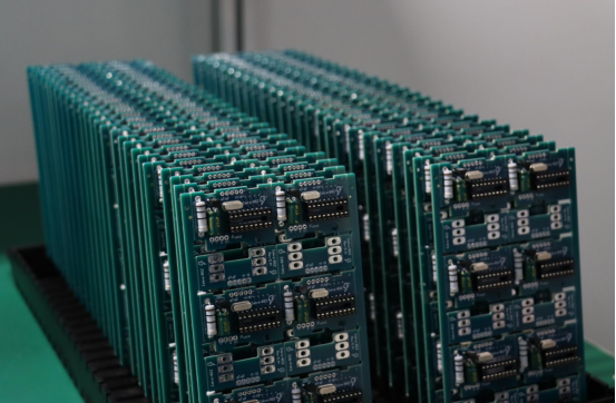
Main PCB Assembly: A Complete Guide for Beginners and Professionals
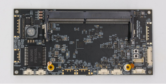
Main PCB assembly refers to the process of assembling the primary printed circuit board that integrates all the key components of an electronic device. This board acts as the “central hub,” connecting microcontrollers, power circuits, connectors, and other essential parts into one functional system. Without a well-designed main PCB assembly, even the best electronic components cannot work together properly.
Main PCB assembly matters because it directly affects a product’s performance, reliability, and production cost. A precise assembly ensures signal integrity, stable power delivery, and longer device lifespan. For example, in a smartphone, the main PCB assembly determines how the processor, memory, and sensors communicate efficiently. In an industrial controller, it ensures consistent operation under demanding conditions.
This guide is designed for engineers, product designers, procurement specialists, and even beginners who want a clear understanding of how main PCB assembly works. Whether you are developing a new IoT device, sourcing PCBs for mass production, or simply learning the basics, this article will give you a step-by-step overview and practical insights to make informed decisions.
What Is Main PCB Assembly?
Definition and Purpose
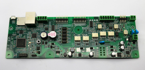
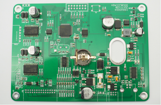
Main PCB assembly is the process of placing and soldering electronic components onto the primary printed circuit board (PCB) of a device. This is different from PCB manufacturing, which only produces the bare board — the fiberglass substrate with copper traces. Assembly is the stage where the board becomes functional by adding microchips, resistors, capacitors, connectors, and other parts.
The main PCB serves as the central control hub of an electronic product. It distributes power, enables communication between components, and ensures that signals are routed correctly. Without a properly assembled main PCB, the device cannot function as intended.
For example:
In a smartphone, the main PCB links the processor, memory, battery management system, and wireless modules.
In industrial controllers, it coordinates sensors, relays, and output drivers to automate processes.
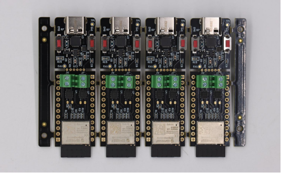
In IoT devices, it connects the microcontroller, Wi-Fi or Bluetooth module, and power supply in a compact design.
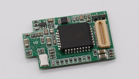
Key Components in Main PCB Assembly
A main PCB assembly typically includes the following essential components:
Microcontroller or Processor: Acts as the “brain” of the device, handles data processing, logic control, and communication with peripherals.
Power Management Circuits: Regulate and distribute power from the battery or power supply, protect against overcurrent, overvoltage, and thermal issues.
Connectors and Interfaces: Provide input/output connections (USB, HDMI, pin headers), enable communication with external devices or modules.
Passive Components (resistors, capacitors, inductors): Stabilize voltage, filter noise, and control current flow, ensure consistent and reliable performance of the circuit.
Each of these elements plays a critical role in making the PCB a fully functional “main board” that supports the entire product.
Types of Main PCB Assemblies
Single-Sided vs. Double-Sided Assemblies
A single-sided PCB assembly has all copper traces and components mounted on one side of the board. This makes it cost-effective and easy to manufacture, which is why it is common in simple consumer products such as calculators or power adapters.
A double-sided PCB assembly has copper traces on both sides, allowing more components to fit into a smaller area. This design is ideal for more complex devices like home appliances, industrial controllers, and communication modules.
Cost Comparison: Single-sided assemblies are cheaper due to simpler production steps. Double-sided boards cost more but allow higher component density and better electrical performance.
Through-Hole vs. Surface-Mount (SMT) Assembly
Through-hole assembly involves inserting component leads into drilled holes and soldering them to the board.
Advantages: Very strong mechanical bond, good for connectors, transformers, and components exposed to stress.
Disadvantages: Slower, more expensive, and takes up more board space.
Surface-mount technology (SMT) uses tiny pads on the surface of the PCB where components are placed and soldered.
Advantages: Enables smaller, lighter designs and supports high-speed automated assembly.
Disadvantages: Components can be harder to replace by hand, and mechanical strength is lower than through-hole.
When to choose:
Use through-hole for high-power components, connectors, and devices that need durability.
Use SMT for miniaturized, high-volume products like smartphones and IoT modules.
Mixed Technology Assemblies
Many products use mixed technology PCB assemblies, combining both SMT and through-hole methods.
Examples:
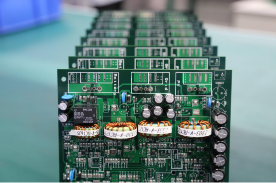
Power supplies often use SMT for control circuits and through-hole for large capacitors or connectors.
Automotive modules use SMT for sensors and logic chips but through-hole for relays and heavy components.
Benefits:
Achieves compact design without sacrificing mechanical strength.
Balances manufacturing cost with performance and durability.
Main PCB Assembly Process
The main PCB assembly process transforms a bare circuit board into a fully functional mainboard by adding and soldering all required components. Below is a step-by-step explanation of each stage.
Step 1: Design and BOM Preparation
The process begins with PCB layout design. Engineers carefully arrange traces, pads, and component locations to ensure good signal integrity, power distribution, and thermal performance. Proper spacing between components helps avoid short circuits and makes automated assembly easier.
Next comes the Bill of Materials (BOM) — a complete list of all components needed for the assembly. Accuracy is crucial:
Incorrect part numbers can delay production.
Choosing parts that are readily available helps avoid supply chain issues.
Verified BOM data ensures cost control and smooth procurement.
Step 2: Solder Paste Printing
Before components are mounted, solder paste is applied to the board using a stainless-steel stencil. This stencil has cutouts that match the pad locations.
Why it matters: Precise paste deposition is critical because too much paste can cause solder bridging, while too little can result in weak or open connections. High-quality printers ensure consistent application, improving overall assembly yield.
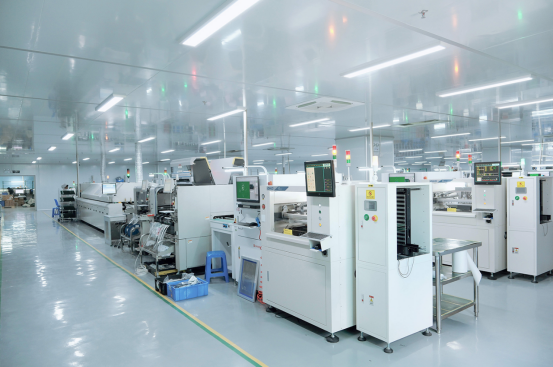
Step 3: Pick-and-Place Assembly
Automated pick-and-place machines then place components on the board.
The machine reads coordinate data from the PCB design files.
Components are picked from reels or trays and placed with high speed and accuracy — sometimes tens of thousands of placements per hour.
This step is essential for ensuring that every part is positioned correctly before soldering.
Step 4: Soldering
Once all components are in place, soldering permanently attaches them to the PCB. There are three main techniques:
Reflow Soldering (SMT): The board passes through a controlled-temperature oven that melts the solder paste, forming strong electrical connections.
Wave Soldering (Through-Hole): The underside of the board is passed over a wave of molten solder to attach through-hole components.
Selective Soldering (Mixed Technology): Used when only certain areas need through-hole soldering, preventing damage to nearby SMT parts.
Each method is chosen based on the component type and assembly requirements.
Step 5: Inspection and Quality Control
Quality control ensures that the assembled PCB meets performance and safety standards.
AOI (Automated Optical Inspection): Cameras scan the board to detect missing parts, polarity errors, or solder defects.
X-ray Inspection: Used for hidden joints like BGAs (Ball Grid Arrays) where visual inspection is impossible.
In-Circuit Testing (ICT) and Functional Testing: Measure electrical continuity, verify component values, and ensure the board performs as expected under real-world conditions.
Thorough inspection prevents defective boards from reaching customers and reduces costly rework.
This structured process ensures that every main PCB assembly is consistent, reliable, and ready for integration into the final product.
Materials and Tools Used in PCB Assembly
Understanding the materials and tools used in PCB assembly is key to ensuring high-quality, reliable mainboards. The right combination of substrates, equipment, and inspection methods directly affects product performance and yield.
PCB Materials
The base material of a PCB affects its strength, heat resistance, and electrical performance.
FR-4: The most common material, made of woven fiberglass and epoxy resin. It offers good mechanical stability and is cost-effective, making it suitable for most consumer electronics.
High-Tg Materials: These materials have a higher glass transition temperature, which means they can withstand higher reflow oven temperatures without warping. Ideal for high-power devices or environments with elevated heat.
Flexible Substrates: Thin, bendable materials such as polyimide are used in flexible PCBs. They are critical for compact devices, wearables, and applications where space saving or motion tolerance is important.
How material choice affects performance:
High-frequency devices benefit from low-loss materials that minimize signal degradation.
High-temperature environments require high-Tg laminates to avoid delamination or failure.
Flexible substrates allow creative product designs where rigid boards cannot fit.
Assembly Tools and Equipment
PCB assembly relies on precise, automated equipment to achieve consistent results:
Solder Paste Printer: Deposits solder paste accurately on pads using a metal stencil. Consistency at this stage reduces solder defects.
Pick-and-Place Machines: Automatically place components on the board with speed and accuracy, supporting both small SMT parts and larger IC packages.
Reflow Oven: Heats the board in controlled stages to melt solder paste and create strong electrical connections.
Wave Soldering Machine: Used for through-hole components, where a wave of molten solder bonds all leads in a single pass.
Inspection Tools (AOI, X-ray): Ensure quality by detecting missing, misaligned, or poorly soldered parts. X-ray inspection is critical for hidden joints like BGAs.
By combining the right materials with the proper equipment, manufacturers achieve reliable PCB assemblies that meet performance, durability, and cost targets.
Best Practices for High-Quality Main PCB Assembly
High-quality main PCB assembly starts with good design, reliable sourcing, and strict adherence to quality standards. Following these best practices ensures better performance, fewer defects, and lower production costs.
Design for Manufacturability (DFM)
Design for Manufacturability (DFM) means creating a PCB layout that is easy to produce, inspect, and assemble without costly rework.
Spacing: Maintain adequate clearance between pads, traces, and components to prevent solder bridging or short circuits.
Pad Design: Use correctly sized pads and land patterns that match component specifications for better solder joints.
Thermal Reliefs: Include thermal reliefs on copper pours to improve solderability and heat dissipation.
Avoiding common layout issues:
Do not place components too close to board edges.
Minimize trace length for high-speed signals to reduce noise.
Add fiducial marks for pick-and-place machine alignment.
By applying DFM principles, you reduce production errors and improve assembly yield.
Component Selection and Sourcing
Choosing the right components and suppliers is critical for consistent production quality.
Reliable Suppliers: Work with suppliers that provide traceability, datasheets, and proven quality records.
Component Availability: Check lead times and stock levels early to avoid delays or expensive last-minute substitutions.
Lifecycle Management: Select components that are not near end-of-life (EOL) to ensure long-term support for your product.
Example: Replacing a microcontroller mid-production due to shortages can require PCB redesign, delaying product launches.
Quality Standards and Certifications
Adhering to international quality standards ensures that assemblies meet industry requirements.
IPC-A-610: Defines the acceptability criteria for solder joints, component placement, and overall assembly quality.
ISO 9001: Demonstrates that the manufacturer follows consistent quality management systems.
RoHS Compliance: Confirms that assemblies are free of hazardous substances like lead, aligning with environmental regulations.
These standards not only improve reliability but also help products pass regulatory testing faster and enter global markets without compliance issues.
Common Challenges and How to Solve Them
Even with careful planning, main PCB assemblies can face quality and reliability challenges. Understanding the root causes and applying proven fixes helps manufacturers maintain high yields and reduce rework costs.
Soldering Defects
Soldering defects are among the most common issues in PCB assembly.
Tombstoning: Happens when one end of a small component lifts during reflow, leaving it standing upright.
Cause: Uneven solder paste volume or temperature gradient between pads.
Solution: Ensure stencil design has equal aperture sizes and maintain consistent oven profiles.
Bridging: Occurs when excess solder forms a bridge between adjacent pads, creating a short circuit.
Cause: Too much solder paste, poor stencil alignment, or excessive reflow temperature.
Solution: Optimize solder paste deposition and reflow parameters, and use proper pad spacing.
Cold Joints: Weak or dull-looking solder connections that can lead to intermittent failures.
Cause: Insufficient heat during soldering or contaminated surfaces.
Solution: Clean PCB surfaces, verify reflow oven calibration, and ensure proper flux activation.
Component Misalignment
Component misalignment happens when parts are not placed correctly on pads before soldering.
Causes: Pick-and-place machine inaccuracy, worn nozzles, or vibration during transport.
Solutions:
Use vision systems in assembly machines to verify placement.
Regularly calibrate and maintain pick-and-place equipment.
Optimize board handling to prevent shifting before reflow.
Correct alignment ensures reliable solder joints and avoids costly manual rework.
Thermal Management Issues
Poor heat management can cause overheating, component failure, or reduced product lifespan.
Heat Dissipation Techniques:
Add thermal vias to spread heat to inner copper layers.
Use heat sinks or thermal pads for high-power components like regulators or MOSFETs.
Design wider copper traces for power circuits to reduce heat buildup.
Impact on Reliability: Excessive heat can cause solder joint fatigue, drift in component performance, and even catastrophic failure in power electronics. Effective thermal design improves product stability and long-term reliability.
Choosing a Main PCB Assembly Partner
Selecting the right PCB assembly partner is crucial for ensuring product quality, timely delivery, and long-term reliability. The right partner combines technical expertise with production capabilities and strong quality management.
Factors to Consider
Experience with Similar Products:
Choose a partner who has worked with products similar to yours. For example, if you are producing compact IoT devices, a partner experienced in high-density SMT assembly will better handle small components and fine-pitch layouts.
Production Capacity and Lead Times:
Ensure the manufacturer can meet your production volumes and deadlines. A small-capacity assembler may struggle with high-volume orders, causing delays or quality compromises.
Quality Certifications:
Check for recognized certifications such as IPC-A-610, ISO 9001, and RoHS compliance. These demonstrate adherence to international quality standards and regulatory requirements. Certified partners are more likely to produce consistent, defect-free assemblies.
Cost vs. Quality Balance
Why Cheapest Is Not Always Best:
Extremely low-cost suppliers may cut corners on material quality, inspection, or assembly processes, which can lead to higher defect rates and reliability issues.
Total Cost of Ownership Perspective:
Consider not just unit price but the overall cost of defects, rework, delayed delivery, and product recalls. A slightly higher upfront cost with a reputable partner often results in lower long-term expenses and better product reliability.
By evaluating these factors carefully, you can choose a main PCB assembly partner that aligns with your technical requirements, production timeline, and quality expectations, ensuring your products perform reliably in the field. For businesses looking for a trusted and experienced partner, PCBMASTER offers comprehensive PCB assembly solutions—from prototyping to full-scale production—backed by quality certifications and advanced manufacturing capabilities. Partnering with PCBMASTER can help streamline your production process and deliver consistent, high-quality results.
Future Trends in Main PCB Assembly
The field of main PCB assembly is evolving rapidly due to advances in miniaturization, high-density designs, and automation. Staying aware of these trends helps manufacturers and designers improve efficiency, reduce costs, and maintain product reliability.
Miniaturization and High-Density Interconnect (HDI)
Miniaturization involves making PCBs smaller while increasing component density, which is essential for modern electronics like smartphones, wearables, and compact IoT devices.
High-Density Interconnect (HDI) PCBs use finer traces, smaller vias, and microvias to connect components in tightly packed spaces.
Impact on Main PCB Design: Designers must carefully plan signal routing, layer stack-up, and thermal management to handle increased complexity.
Opportunities: Smaller devices, lighter products, and more functionality in the same board area.
Challenges: Requires advanced manufacturing equipment, precise assembly processes, and rigorous inspection to avoid defects.
Automation and AI in Assembly
Automation and artificial intelligence (AI) are transforming PCB assembly by improving speed, accuracy, and predictive capabilities.
Predictive Maintenance for Pick-and-Place Machines: AI systems analyze equipment performance and predict failures before they occur, reducing downtime and unexpected production delays.
AI-Based Inspection Systems: Machine learning enhances Automated Optical Inspection (AOI) and X-ray systems by detecting subtle defects, such as misaligned components or solder voids, that traditional inspection might miss.
These technologies reduce human error, improve yield, and enable scalable, high-volume production of complex main PCB assemblies.
Conclusion
Main PCB assembly is the foundation of every reliable electronic device. From smartphones to industrial controllers, the main PCB acts as the central hub that connects processors, power circuits, sensors, and interfaces. High-quality assembly ensures proper signal flow, stable power distribution, and long-term device reliability, making it a critical step in product development and manufacturing.
To achieve consistent, high-quality results, it is essential to work with experienced PCB assembly partners who understand design complexities, follow industry standards, and use advanced assembly and inspection equipment. Whether you are an engineer, product designer, or procurement professional, choosing the right partner can save time, reduce costs, and ensure your product performs as intended.
For anyone looking to learn more, consult an expert, or request a PCB assembly quote, professional PCB suppliers like PCBMASTER offer comprehensive solutions, from prototyping to full-scale production. Contacting a trusted provider ensures your main PCB assemblies meet both technical and quality expectations, helping you bring your products to market faster and with confidence.
FAQs
1. What is the difference between PCB fabrication and PCB assembly?
PCB fabrication refers to the process of producing the bare printed circuit board itself. This includes:
Creating the copper traces on the substrate (e.g., FR-4, flexible materials).
Drilling holes for through-hole components.
Applying solder masks, silkscreen markings, and surface finishes (like HASL or ENIG).
PCB assembly, on the other hand, is the process of adding electronic components to the fabricated PCB to make it functional. It includes:
Solder paste printing for SMT pads.
Pick-and-place assembly of components.
Soldering using reflow, wave, or selective soldering.
Inspection and testing to ensure the board works as designed.
In short: fabrication creates the empty board; assembly turns it into a working circuit.
2. How do I choose the right PCB assembly process for my project?
The right assembly process depends on the component type, product complexity, volume, and mechanical requirements:
Surface-Mount Technology (SMT): Best for small, compact components and high-volume production. Offers faster automated assembly and reduced board size.
Through-Hole Assembly: Strong mechanical bonds, ideal for connectors, large capacitors, or components exposed to stress. Slower and more expensive than SMT.
Mixed Technology Assembly: Combines SMT and through-hole for boards that require both miniaturization and mechanical strength. Common in power electronics and industrial applications.
Decision tips:
For high-density boards, SMT enables compact layouts and fast automated assembly.
Through-hole is best for heavy or high-stress components needing strong mechanical support.
A mixed approach works when both SMT and through-hole parts are used, balancing size and strength.
Always consider design for manufacturability (DFM) principles to simplify assembly.
3. What are the most common defects in PCB assembly and how can I avoid them?
Common PCB assembly defects include:
Tombstoning: One end of a small component lifts during reflow.
Cause: Uneven solder paste or temperature variation.
Prevention: Proper stencil design and controlled oven profiles.
Solder Bridging: Excess solder connects adjacent pads.
Cause: Over-application of solder paste or poor pad spacing.
Prevention: Optimize solder paste deposition and pad layout.
Cold Joints: Weak or dull solder connections.
Cause: Insufficient heat or contaminated surfaces.
Prevention: Clean PCB surfaces, check oven calibration, and use proper flux.
Component Misalignment: Parts not properly placed on pads.
Cause: Pick-and-place errors or vibrations.
Prevention: Use vision systems, regular calibration, and careful handling.
Thermal Issues: Overheating or poor heat dissipation.
Prevention: Add thermal vias, heat sinks, and properly sized copper traces.
Routine inspection techniques like AOI, X-ray, and in-circuit testing help detect defects early.
4. How much does main PCB assembly cost on average?
PCB assembly costs vary depending on board size, complexity, components, and production volume:
Prototype/low-volume assembly: $50–$300 per board (cost increases with component density and special parts).
Small batch production (10–100 boards): $20–$100 per board on average.
Mass production (>1,000 boards): Costs can drop to $5–$30 per board depending on assembly type (SMT is cheaper at scale).
Factors influencing cost:
Number of SMT vs. through-hole components.
PCB layer count and board size.
Quality standards and certifications (IPC, RoHS compliance).
Testing requirements (functional testing, ICT, AOI).
Tip: Always consider total cost of ownership, including potential rework and defect management, not just the unit price.
5. Can small businesses or hobbyists order main PCB assembly in low volumes?
Yes, many PCB assembly service providers support low-volume orders, often starting from just 1–5 boards.
Benefits for small businesses/hobbyists:
Test prototypes before scaling production.
Reduce upfront investment in pick-and-place machines or soldering equipment.
Access high-quality professional assembly that might be difficult to achieve manually.
Considerations:
Lead times may be slightly longer for small orders.
Component costs may be higher for low quantities.
Many suppliers offer turnkey solutions, including sourcing, assembly, and testing.
Example: Companies like PCBMASTER provide low-volume, high-quality main PCB assembly services suitable for prototyping, startups, and hobbyist projects.

