


Effective Impedance Control Essential Tips for Reliable PCB Design
Introduction
Impedance control is vital for maintaining signal integrity in PCBs. It involves managing trace impedance to avoid distortions. Learn what impedance control is, why it matters, and how to implement it.
Key Takeaways
·Impedance control is crucial for maintaining signal integrity in high-frequency PCB designs, preventing issues such as signal reflections and timing errors.
·Key factors influencing impedance control include trace width, dielectric materials, and layer stackup configuration, which all play a significant role in achieving target impedance values.
·Collaboration with PCB manufacturers, along with the use of specialized tools like impedance calculators and simulation software, is essential for ensuring that PCB designs meet the desired impedance specifications.
Understanding Impedance Control

Impedance control is not merely a technical term; it’s a critical aspect of PCB design that protects signals and manages their impedance to avoid errors. Controlled impedance in high-frequency applications ensures reliable signal transmission, preventing issues that could compromise design integrity.
But what exactly is impedance control, and why has it become so important in recent years? As electronic components operate at increasingly higher frequencies, even small deviations in impedance can significantly affect signal integrity.
Exploring the fundamentals of impedance control provides a solid foundation for understanding its role in high-speed circuit performance and reliability.
What is Impedance Control?
At its core, impedance control involves measuring the impedance of PCB traces and ensuring they meet the designer’s specified limits. Controlled impedance refers to the characteristic impedance of transmission lines formed by PCB traces and reference planes, which is crucial for maintaining signal integrity. Impedance, defined as the opposition of a circuit to alternating current, is measured in Ohms and is influenced by PCB materials and the dielectric constant.
Controlled impedance helps PCB designers create reliable high-speed circuit boards by minimizing signal reflections and timing errors. With the increasing frequencies of electronic components, precise pattern dimensions and placements are essential to maintain consistent performance and avoid issues such as signal distortion and increased switching times.
Why Impedance Control Matters
High-frequency applications demand controlled impedance to maintain signal clarity and prevent data loss. Without it, signal reflections and distortions can occur, severely impacting the performance and reliability of the circuit. Signals operating at frequencies above 100 MHz, such as RF communication and high-speed digital interfaces, are particularly sensitive to impedance variations.
PCB designers must achieve target impedance values with tight tolerances when working with high-frequency signals. Considering controlled impedance during the design phase significantly improves signal integrity, reduces the potential for signal distortion, and ensures reliable performance.
Key Factors Influencing Impedance Control
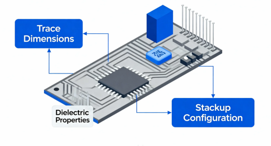
Several key factors influence impedance control in PCB design. Controlled impedance is essential for managing signal reflections and ensuring effective transmission at high frequencies. High-speed digital applications, RF communication, and high-quality analog video all require precise impedance control to function correctly.
The characteristic impedance of PCB traces is influenced by their physical dimensions, such as thickness, width, and height, as well as the dielectric materials used. Advanced simulation tools can help visualize signal integrity and analyze potential distortions, aiding designers in maintaining consistent impedance across different trace geometries and production batches.
Delving into the main factors affecting impedance control offers insights into effective force management.
Trace Width and Thickness
Trace width and thickness are critical in achieving specific impedance values because:
·Trace width adjustments directly impact the electrical characteristics of the PCB, making it essential for impedance control.
·The typical range of trace impedance on PCBs is between 25 and 125 Ohms.
·For high-speed differential pairs, specific trace width and spacing are required to calculate differential impedance accurately. Additionally, the copper weight can influence these parameters, including trace thickness.
Choosing the right materials is crucial for trace width calculations needed to meet impedance goals. Stackup calculators can assist designers in determining the appropriate trace widths to achieve their impedance targets. Careful management of trace geometries and materials ensures PCB designs meet the desired impedance specifications.
Dielectric Constant and Materials
The dielectric constant and material selection play a vital role in achieving specified impedance in PCB layouts. The dielectric constant of the PCB material influences the impedance characteristics of the traces, making it a crucial parameter in impedance control. Composite PCB models in impedance calculators allow designers to work with multiple dielectric materials for better precision.
Some impedance calculators enable users to input material properties, providing accurate predictions of impedance values. Adopting a controlled dielectric approach and selecting appropriate materials helps achieve the desired impedance and ensures the reliability of high-frequency PCB designs.
Layer Stackup Configuration
Proper layer stackup is essential for maintaining target impedance values, especially for high-frequency signals. The configuration of PCB layers impacts impedance, and a well-designed stackup can help mitigate variations and maintain consistent impedance levels. Early communication with fabricators is crucial to understand standard stackups and design rules, avoiding costly design changes later.
Careful layer configuration and collaboration with fabricators ensure PCB designs meet the desired impedance specifications, resulting in reliable and high-performing circuits.
Designing for Controlled Impedance
Designing for controlled impedance requires:
·A thorough understanding of the factors affecting impedance
·The use of specific software tools to establish requirements for impedance control
·Utilizing a variety of specialized tools and resources tailored for PCB designers to achieve effective impedance control
Exploring strategies for designing PCBs with controlled impedance includes identifying critical signals, calculating impedance, and accurately annotating design files.
Identifying Critical Signals
Certain signals require controlled impedance. Examples of these include:
·DDR
·HDMI
·Gigabit Ethernet
·RF signals
Designers can determine which signals need controlled impedance by reviewing datasheets of integrated circuits. Identifying critical signals early in the design process ensures PCB layouts meet the necessary impedance requirements for reliable performance.
Calculating Impedance
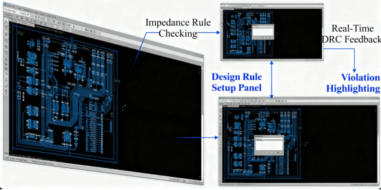
Calculating impedance values accurately is essential for achieving target impedance in PCB designs. Designers can utilize advanced electronics CAD tools to model and calculate the impedance values required for different traces. Impedance calculators assist in determining the necessary trace dimensions to match specified impedance requirements.
Leveraging these tools ensures PCB designs meet the desired impedance specifications, resulting in reliable signal transmission and reduced potential for signal distortion.
Annotating Design Files
Clear annotations in design files are crucial to avoid miscommunication during manufacturing. Key points to include in design annotations are:
·Accurately identifying controlled impedance traces so manufacturers can modify widths as needed.
·Including specific impedance values for different types of signals.
·Specifying whether nets are single-ended or differential pairs along with their respective impedance values.
Providing clear and detailed annotations ensures impedance requirements are understood and met during the manufacturing process.
Implementing Differential Impedance
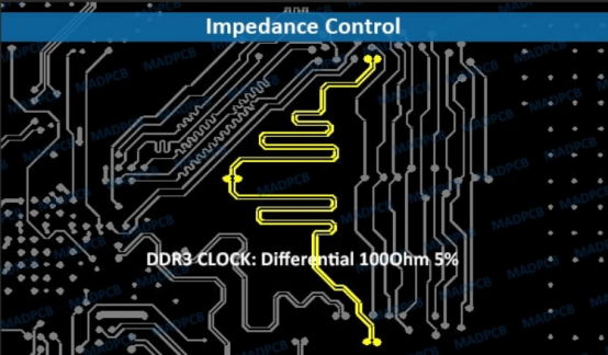
Implementing differential impedance is crucial for maintaining consistent signal integrity in high-speed applications. Routing differential pairs requires careful attention to achieve the desired differential impedance and avoid potential signal degradation.
Covering best practices for routing differential pairs similarly includes maintaining symmetry and proper spacing.
Routing Differential Pairs
Routing differential pairs involves several best practices to ensure reliable signal performance:
·Length matching is essential to achieve propagation delay matching and avoid unacceptable delay skew.
·Using serpentines on the shorter trace can compensate for mismatches in length.
·Minimize the use of vias.
·If vias are used, ensure symmetry.
Placing components between differential pairs creates impedance discontinuity, leading to signal integrity issues. Stitching vias should be added close to signal vias when a high-speed differential pair switches layers.
Following these practices helps achieve proper differential impedance and maintain signal integrity.
Symmetry and Spacing
Maintaining symmetry in differential pair routing is essential to minimize signal integrity issues and ensure consistent impedance. The importance of symmetry in routing differential pairs cannot be overstated, as it helps achieve the desired impedance targets and reliable performance.
Proper spacing between differential pairs is crucial for avoiding crosstalk and ensuring reliable signal transmission.
Collaborating with PCB Manufacturers
Effective collaboration with PCB manufacturers is vital for achieving the desired impedance specifications in your designs. Clear communication of impedance requirements helps avoid manufacturing confusion and ensures product quality.
Highlighting the importance of detailed specifications and early engagement with fabricators is crucial.
Providing Detailed Specifications
Including detailed stackup tables with trace widths is crucial for achieving specific impedance values. Providing an impedance table summarizing the specifications for each layer in the fabrication drawing can simplify communication and ensure the PCB meets design targets. It’s also essential to specify impedance values and trace dimensions in the fabrication notes.
Clearly defining tasks and requirements in the statement of work (SOW) and including impedance tables during PCB fabrication ensures specifications are understood and met by manufacturers in the task space stiffness.
Working with Fabricators
Early engagement with fabricators allows designers to understand standard stackup options and avoid costly design modifications later. Manufacturers handle controlled impedance requirements by calculating feasible thickness, width, and height. If a fabricator does not support the required trace widths, it’s advisable to seek out another fabricator with suitable capabilities.
Working closely with fabricators ensures they can meet design needs, achieving the desired impedance specifications and reliable pcb manufacturer.
Tools and Resources for Impedance Control
Designers have access to specialized tools and resources for impedance control, which are crucial for ensuring reliable performance in PCB designs. These tools help determine the right trace widths and other parameters essential for achieving the desired impedance.
Introducing impedance calculators and simulation software offers valuable resources for impedance calculation for designers.
Impedance Calculators
Impedance calculators are invaluable tools for determining the precise trace dimensions needed to achieve specific impedance values. Sierra Circuits’ impedance calculator, for instance, offers:
·A 2D numerical solution of Maxwell’s equations to determine impedance values
·Various microstrip and stripline structures
·Support for single-ended and differential models
These calculators not only estimate impedance but also provide insights into:
·Capacitance
·Inductance
·Propagation delay per unit length
·Effective dielectric constant
Leveraging these tools ensures PCB designs meet the desired impedance specifications, resulting in a reliable signal output ratio transmission and reduced potential for signal distortion.
Simulation Software
Simulation software is another critical resource for impedance control, allowing designers to:
·Model PCB designs and predict impedance behavior under various electrical conditions.
·Perform pre-layout analyses to estimate impedance and design parameters before the final PCB layout.
·Identify potential issues early on.
Post-layout verification using simulation software confirms that actual PCB designs align with intended impedance values, ensuring reliable performance. Utilizing 2D and 3D electromagnetic field solvers provides precise impedance values and S-parameters, enhancing the accuracy and reliability of the design.
Ensuring Quality and Compliance
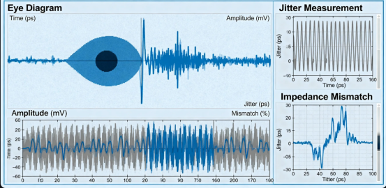
Quality assurance is paramount in maintaining impedance control across production batches. Implementing test coupons in PCB designs allows for efficient verification of impedance during the manufacturing process. Testing and verification methods, such as Time Domain Reflectometry (TDR) and Vector Network Analyzers (VNAs), are critical to ensuring that PCBs meet desired impedance specifications and provide value.
Ongoing quality assurance practices are necessary to identify potential issues early, ensuring consistent performance and compliance with design specifications. Employing effective testing methods throughout the manufacturing process ensures PCB designs meet the highest standards of reliability and performance.
Testing and Verification
Testing impedance is crucial due to the length of traces, which is influenced by the PCB size. Time Domain Reflectometry (TDR) is a primary method used to test PCB impedance by analyzing reflected signals. Vector Network Analyzers (VNAs) measure impedance across a frequency range, making them suitable for RF applications.
If an impedance coupon fails the test, Sierra Circuits conducts impedance testing on boards to check compliance with specifications. The location of inner layer impedance traces is critical to ensuring the finished PCB meets impedance specifications.
Utilizing these testing methods ensures PCB designs meet the desired impedance targets.
Quality Assurance Practices
Quality assurance is essential in PCB design to ensure that each production batch meets the desired performance standards. Implementing test coupons in PCB designs allows for efficient verification of impedance during the manufacturing process. Employing effective testing methods throughout the PCB manufacturing process can identify potential issues early, ensuring consistent quality.
Maintaining rigorous quality assurance practices ensures PCB designs consistently meet impedance specifications, resulting in reliable and high-performing circuits.
Summary
In summary, effective impedance control is crucial for ensuring reliable signal transmission and maintaining the integrity of high-frequency PCB designs. By understanding the fundamentals of impedance control, identifying critical signals, calculating impedance accurately, and collaborating effectively with PCB manufacturers, designers can achieve the desired impedance specifications and ensure the performance and reliability of their circuits.
The journey to mastering impedance control involves leveraging advanced tools and resources, implementing best practices for routing differential pairs, and maintaining rigorous quality assurance practices. As you continue to refine your PCB designs, remember that achieving consistent impedance control is key to unlocking the full potential of your high-frequency applications. Embrace the challenge, and let your designs soar to new heights of performance and reliability.
FAQs
Q.Why is controlled impedance important in PCB design?
A.Controlled impedance is essential in PCB design to ensure signal integrity and reduce the risk of signal reflections and distortions, particularly in high-frequency applications. This practice enhances performance and reliability in electronic circuits.
Q.How can I calculate the impedance of PCB traces?
A.To calculate the impedance of PCB traces, one should utilize advanced electronics CAD tools and impedance calculators, which will model and provide the necessary impedance values for reliable signal transmission. This approach ensures accuracy in your design.
Q.What are some best practices for routing differential pairs?
A.To achieve optimal performance with differential pairs, it is crucial to implement best practices such as length matching, minimizing via usage, maintaining symmetry, and ensuring proper spacing for desired differential impedance. Adhering to these guidelines will help prevent signal integrity issues.
Q.How can I ensure my PCB designs meet the desired impedance specifications during manufacturing?--H3
A.To ensure your PCB designs meet the desired impedance specifications during manufacturing, clearly communicate your impedance requirements, provide detailed specifications, and collaborate closely with your PCB manufacturer. This proactive approach will help achieve the desired results.
Q.What testing methods are used to verify impedance in PCBs?
A.Time Domain Reflectometry (TDR) and Vector Network Analyzers (VNAs) are essential methods for verifying impedance in PCBs, ensuring that they meet design specifications and perform reliably.
Author: Jack Wang

