


Understanding PCB Quality Requirements: A Comprehensive Guide for Electronics
Printed Circuit Boards (PCBs) are the backbone of modern electronic devices. They provide the physical structure and electrical pathways that connect and support components like microchips, capacitors, and resistors. Without PCBs, devices like smartphones, computers, and medical equipment wouldn’t function as we know them today.
The quality of a PCB is crucial for ensuring that the electronic devices it supports work reliably over time. A high-quality PCB guarantees that electrical signals flow correctly, preventing issues like short circuits or component failure. It also affects how long a device lasts, especially in environments with high temperatures, humidity, or physical stress.
This guide will explore the key PCB quality requirements that electronics manufacturers must meet to produce reliable and durable circuit boards. We’ll focus on industry standards, testing methods, and best practices that ensure high performance and longevity. Whether you’re designing or sourcing PCBs, understanding these quality requirements is essential for producing top-tier electronic products.

What Are PCB Quality Requirements?
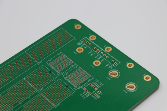
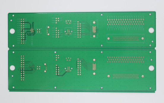
PCB quality requirements refer to the specific standards, criteria, and specifications that determine how well a PCB is designed, manufactured, and tested. These requirements are crucial to ensure that PCBs perform their intended functions reliably within electronic devices. They cover various aspects, including electrical conductivity, physical durability, and manufacturing precision. Key standards for PCB quality include IPC-610 for acceptability criteria and IPC-2221 for design. These documents define the acceptable limits for factors such as trace width, hole placement, and component alignment. Manufacturers must meet these standards to produce functional and durable PCBs that can withstand the stresses of daily use.
Meeting PCB quality standards is vital for ensuring the long-term performance of electronic devices. A well-made PCB ensures that electrical components are connected properly and signals flow smoothly without interruption. For example, high-quality PCBs in smartphones prevent malfunctioning or overheating, allowing them to function correctly over extended periods.
Poor-quality PCBs can lead to device failures, such as short circuits, incorrect signal transmission, or even complete device breakdowns. In industries like automotive or medical equipment, this can result in costly recalls, safety hazards, or even loss of life. For instance, a faulty PCB in a car’s braking system can be life-threatening. Therefore, adhering to strict quality standards minimizes the risk of operational failures and boosts customer satisfaction by ensuring reliability and durability.
Why Are PCB Quality Requirements Crucial in Electronics Manufacturing?
In electronics manufacturing, ensuring PCB quality is essential for the reliability and longevity of devices. High-quality PCBs directly impact the performance of electronic products, from everyday gadgets like smartphones to critical systems in automotive and medical devices. Without meeting strict quality standards, poor PCBs can lead to failures, safety risks, and costly recalls.
Ensuring Reliability and Durability
Ensuring the reliability and durability of PCBs is crucial for the long-term functionality of electronic devices. Quality standards ensure that PCBs are manufactured to withstand everyday usage and environmental factors such as heat, moisture, and vibrations. For example, a well-designed PCB in a laptop helps prevent overheating and ensures the device continues to function over its lifespan without failure.
One real-life example of poor-quality PCBs leading to failures occurred with early smartphone models, where faulty PCBs caused overheating, leading to battery failure and, in some cases, device explosions. This resulted in costly recalls and damage to the brand’s reputation. High-quality PCBs, on the other hand, reduce the risk of these issues, leading to longer-lasting and more reliable products.
By adhering to industry standards like IPC-610, manufacturers can ensure their PCBs perform consistently, even under challenging conditions, contributing to the device's overall performance and customer satisfaction.
Compliance with Industry Regulations and Standards
Compliance with global standards is essential for manufacturers to produce PCBs that meet safety, environmental, and performance requirements. Standards such as IPC, ISO 9001, and RoHS set the baseline for quality and environmental impact in PCB manufacturing. IPC-2221 defines design requirements, ensuring that PCBs meet specific mechanical and electrical tolerances.
Different industries have strict compliance requirements to ensure safety and functionality. In the automotive industry, PCBs must adhere to ISO 26262, which addresses the safety of electrical components in critical systems like airbags and braking systems. In the medical device industry, ISO 13485 ensures that PCBs in devices like pacemakers meet rigorous standards for reliability and safety. Compliance with these standards helps manufacturers avoid legal and operational risks, such as product recalls, fines, or safety hazards, while also ensuring that their products perform as expected in critical applications.
What Are the Key PCB Quality Standards and Specifications?
Understanding the key PCB quality standards and specifications is essential for ensuring that printed circuit boards meet the necessary performance, safety, and reliability requirements. These standards guide the design, manufacturing, and testing processes, ensuring that PCBs are functional and durable in various applications.
IPC Standards: A Core Framework
Overview of IPC-2221 (Design standard) and IPC-610 (Acceptability standard)
IPC standards are the backbone of PCB manufacturing. IPC-2221 is a design standard that defines the requirements for designing printed circuit boards and their assembly. It specifies the layout, electrical, and mechanical design rules, ensuring that the PCB will function properly and be manufacturable. On the other hand, IPC-610 focuses on the acceptability of assembled PCBs, detailing the criteria for evaluating the quality of components, soldering, and connections. It provides guidelines for what is considered acceptable during manufacturing and inspection.
How these standards shape the design, manufacturing, and inspection process
By adhering to IPC-2221, designers ensure that the PCB is optimized for manufacturability and functionality. This reduces the chances of design errors, such as improper trace width or insufficient spacing between components. IPC-610 plays a crucial role during the inspection process, helping manufacturers assess the finished product for defects such as solder bridges or misaligned components. Together, these standards guide the entire PCB lifecycle—from design through production and quality control—ensuring the final product meets industry expectations.
ISO Certifications and Their Role in PCB Quality
ISO 9001 and ISO 13485 certifications: What they mean for PCB manufacturers
ISO certifications are globally recognized standards for quality management systems. ISO 9001 ensures that manufacturers implement systematic procedures to maintain consistent product quality. For PCB manufacturers, this certification means they must follow strict internal processes for design, production, and testing, ensuring reliability and customer satisfaction. ISO 13485, specific to medical devices, guarantees that PCBs used in medical equipment meet the highest safety and performance standards, critical for life-saving applications like pacemakers or ventilators.
How certification impacts product quality and customer confidence
ISO certifications demonstrate that a manufacturer is committed to maintaining high standards and consistently producing quality products. This certification provides customers with confidence, knowing that the manufacturer adheres to internationally recognized quality practices. For example, a PCB supplier with ISO 9001 certification is seen as reliable, as it ensures their products meet strict quality criteria consistently. For medical industries, ISO 13485 ensures that the PCBs in medical devices are safe, reducing the risk of device failure and ensuring compliance with regulatory requirements.
Other Relevant Industry Standards
Mention of RoHS, UL certification, and other specific quality standards related to PCBs
Apart from IPC and ISO, there are other critical standards that influence PCB manufacturing. RoHS (Restriction of Hazardous Substances) is an environmental standard that limits the use of harmful materials like lead, mercury, and cadmium in PCBs. This is particularly important for industries aiming for eco-friendly products and compliance with international environmental regulations. UL Certification (Underwriters Laboratories) ensures that PCBs meet safety and fire-resistance standards, making them suitable for use in consumer electronics and industrial applications.
How these standards ensure safety, performance, and environmental responsibility
Standards like RoHS ensure that PCBs are produced with minimal environmental impact, aligning with global sustainability goals. UL certification provides an added layer of assurance that PCBs are safe for use in high-voltage or high-temperature environments. Adhering to these standards not only guarantees product safety but also builds consumer trust, as customers know the products are tested against rigorous safety and environmental criteria. For example, a PCB used in a home appliance with UL certification ensures that the product will perform safely under typical household conditions, reducing risks such as electrical fires or overheating.
How Are PCB Quality Requirements Measured?
Measuring PCB quality is crucial to ensuring that electronic devices perform reliably and safely. To assess whether a PCB meets quality standards, manufacturers use a combination of visual inspections, electrical testing, and environmental stress tests. Each of these methods helps identify potential issues early in the production process, preventing costly failures later on.
Visual Inspection: The First Line of Defense
Importance of visual checks
Visual inspection is the first step in ensuring the quality of a PCB. This process involves checking the physical aspects of the board, such as trace width, component alignment, and soldering quality. If the traces are too narrow, components improperly placed, or solder joints poorly done, the PCB could malfunction, leading to device failure. For instance, an improperly aligned component could cause an electrical short, or weak solder joints could break, leading to poor connectivity.
Tools used for visual inspection
To carry out these checks effectively, manufacturers use various tools. Microscopes help inspectors closely examine tiny features like trace widths and component leads. Automated Optical Inspection (AOI) is an advanced tool that uses cameras to scan the board, detecting defects that may be missed by the human eye. AOI systems can quickly identify issues like misplaced components or soldering problems, ensuring higher consistency and reducing the chances of human error. This method increases the efficiency and accuracy of the inspection process.
Electrical Testing: Ensuring Proper Functionality
Methods of electrical testing
Electrical testing ensures that the PCB is working correctly. Two main types of tests are used: In-Circuit Testing (ICT) and Functional Testing. In-Circuit Testing checks the electrical properties of individual components on the PCB to ensure they are working properly. It helps identify issues like open circuits, short circuits, and incorrect component placement. Functional Testing involves powering up the PCB and testing it in a simulated environment to verify its performance during real-world use.
Ensuring there are no short circuits, opens, or incorrect connections
During these tests, the primary goal is to identify potential electrical failures such as short circuits, which can cause components to overheat or fail, and open circuits, where a component does not connect properly, leading to the device not functioning. Proper electrical testing guarantees that the PCB meets the required performance standards, ensuring that the electronic device operates as expected in its intended environment.
Environmental and Stress Testing
Thermal cycling, vibration testing, and humidity testing
Environmental and stress testing simulates real-world conditions to ensure the PCB will function properly over time. Thermal cycling involves exposing the PCB to extreme temperature changes, which helps test its ability to withstand overheating or freezing. Vibration testing simulates the physical stress a PCB might experience during transport or use in equipment that experiences movement, like vehicles or drones. Humidity testing checks how the PCB behaves when exposed to high moisture levels, which can cause corrosion or damage to sensitive components.
How these tests mimic real-world operating conditions
These tests are essential because they replicate the conditions the PCB will face in actual use. For example, a PCB used in an outdoor device will likely face both high humidity and temperature changes. By stress-testing the PCB before it reaches consumers, manufacturers can ensure its durability and reliability in the field, reducing the risk of failures in critical applications, such as in medical devices or aerospace systems.
What Are the Common PCB Defects and Their Impact on Quality?
PCB defects, even small ones, can have a major impact on the performance and reliability of electronic devices. Whether it's a solder bridge, trace damage, or drill hole misalignment, these issues can lead to malfunctioning products or even complete failure.
Defects in PCB Manufacturing
Common issues: solder bridges, pad lifting, trace damage, and drill hole misalignment
PCBs can develop several defects during the manufacturing process. Solder bridges occur when excess solder connects two adjacent pins, causing short circuits that prevent the PCB from functioning properly. Pad lifting happens when the copper pad that holds a component comes loose, making it difficult or impossible to properly attach the component to the board. Trace damage refers to physical or electrical damage to the copper traces on the PCB, which can disrupt the flow of electrical signals and cause failure. Drill hole misalignment occurs when holes drilled for components do not align correctly with the pads, resulting in poor connections or the inability to mount components correctly.
These defects typically happen due to errors in the manufacturing process, such as improper soldering techniques, poor handling of the PCB, or inaccurate equipment settings. Identifying and addressing these issues early in the production process can prevent costly failures later on.
Impact of These Defects on PCB Performance
How even minor defects can lead to functionality issues or failure
Even small defects can have a significant impact on PCB performance. For example, a solder bridge may appear as a tiny mistake but can cause a short circuit that renders the entire PCB useless. Similarly, pad lifting may cause intermittent connections that result in unreliable performance. Trace damage can alter signal pathways, causing communication breakdowns in electronic devices. Even slight drill hole misalignment can prevent proper connections, resulting in non-functional circuits.
These issues may not always be immediately apparent but can lead to long-term performance problems, such as overheating, erratic behavior, or even complete failure of the electronic device. The consequences of even minor defects can be severe, especially in mission-critical applications like medical devices or automotive systems.
Real-world examples of failed PCBs in different industries
In the automotive industry, a faulty PCB in a vehicle’s braking system can cause dangerous malfunctions, potentially leading to accidents. For instance, a solder bridge in the PCB of an ABS (Anti-lock Braking System) might lead to brake failure, endangering passengers. Similarly, in the consumer electronics sector, a pad lifting issue in a smartphone PCB could result in poor performance, such as connectivity issues or failure to power on. In medical devices, PCB defects can lead to device malfunction, which in some cases may have life-threatening consequences, such as inaccurate readings from a pacemaker.
These examples underscore the importance of rigorous quality control and testing to catch defects early and prevent the risks associated with poor-quality PCBs.
How Can Manufacturers Ensure PCB Quality Control?
Ensuring PCB quality control is essential for producing reliable and high-performing electronic devices. Manufacturers can achieve this by implementing effective design practices, utilizing both automated and manual inspection techniques, and embracing continuous process improvement.
Design for Manufacturability (DFM)
Importance of designing PCBs with quality control in mind
Designing a PCB with quality control in mind from the start is crucial for avoiding issues during the manufacturing process. Design for Manufacturability (DFM) ensures that the PCB layout is optimized for easy and cost-effective production. By considering factors like trace width, hole sizes, and component placement early in the design, manufacturers can avoid potential defects and manufacturing delays. When a design is difficult to manufacture, it increases the chances of errors during production, which can affect the final product's quality and reliability.
Key considerations: trace width, hole sizes, component placement
Several key factors should be considered when designing a PCB. Trace width refers to the thickness of the copper paths that carry electrical signals. If the traces are too narrow, they could cause overheating or signal interference. Hole sizes are also crucial, as misaligned or improperly sized holes can make it difficult to mount components correctly. Component placement affects both the electrical performance and the mechanical integrity of the PCB. A well-placed component reduces the risk of thermal damage and signal degradation, improving the overall quality and reliability of the PCB.
Automated and Manual Inspection Techniques
The balance between manual inspection and automated tools for efficient quality control
To ensure PCB quality, manufacturers must balance both manual inspection and automated tools. Manual inspection involves visually checking the PCB for defects, which can be effective for identifying issues like soldering errors or misalignment. However, automated inspection tools, such as Automated Optical Inspection (AOI) and X-ray inspection, offer greater speed and accuracy in detecting issues like solder bridges, misaligned components, and hidden defects that are harder to spot by the human eye.
Pros and cons of each method in the PCB quality assurance process
Manual inspection allows for human judgment and flexibility in identifying defects but can be time-consuming and prone to errors. It is often used in low-volume production or for checking complex designs. On the other hand, automated tools like AOI offer faster, more consistent results, especially for large-scale production. They can quickly detect common defects but may miss subtle or complex issues that require human expertise. A combination of both methods is often the best approach, using automated tools for routine checks and manual inspection for more intricate or specialized quality control tasks.
Continuous Process Improvement (CPI)
The role of lean manufacturing and Six Sigma in improving PCB production quality
Continuous Process Improvement (CPI) focuses on continuously enhancing manufacturing processes to improve quality and reduce waste. Lean manufacturing principles aim to streamline production by eliminating inefficiencies and focusing on value-added activities. Six Sigma focuses on reducing defects and variability in production processes. Both approaches work together to improve PCB production by enhancing consistency, reducing errors, and lowering costs. By adopting CPI methods, manufacturers can increase yield, reduce rework, and ultimately produce higher-quality PCBs.
Case study examples of companies that successfully improved their PCB quality control systems
One example of successful CPI implementation is Samsung Electronics, which applied Six Sigma principles to improve its PCB manufacturing processes. By focusing on defect reduction and process optimization, they achieved significant reductions in production costs and defects. Another example is Apple, which uses lean manufacturing techniques to optimize its PCB production. By minimizing waste and improving efficiency, Apple ensures that its PCBs meet the highest quality standards, contributing to the overall reliability of its products.
What Role Does PCB Material Play in Quality?
The material used in a PCB plays a crucial role in determining its performance, reliability, and lifespan. Different materials offer unique benefits, from thermal management to electrical performance, making the choice of material essential for specific applications.
Types of PCB Materials and Their Impact on Quality
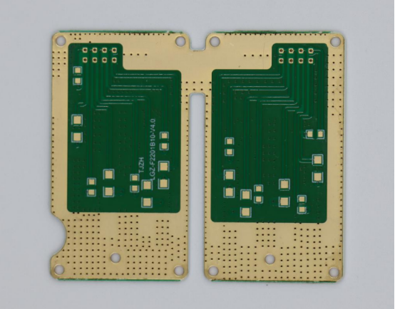
Common materials: FR-4, CEM1, Rogers, and flexible PCBs
The material chosen for a PCB plays a significant role in its overall performance, thermal management, and durability. Some of the most common PCB materials include:
l FR-4: The most widely used material, made from woven fiberglass and epoxy resin. It is cost-effective, reliable, and works well for most general applications.
l CEM1: A cheaper alternative to FR-4, CEM1 consists of a paper-based material and fiberglass. It is commonly used in single-layer PCBs but is less durable than FR4.
l Rogers: This high-performance material is used for applications requiring superior signal integrity and low-loss characteristics, particularly in high-frequency and RF applications.
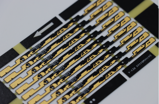
l Flexible PCBs: Made from flexible materials like polyimide, these PCBs are used in applications where bending or conforming to space constraints is necessary.
How material selection affects thermal management, electrical performance, and lifespan
Material choice affects several key aspects of PCB performance. Thermal management is crucial because materials with higher thermal conductivity, like Rogers, help dissipate heat more efficiently, preventing overheating of components. In contrast, FR4 has moderate thermal conductivity but may not be ideal for high-power applications. Electrical performance is impacted by the material’s ability to transmit signals with minimal loss. Materials like Rogers are specially designed for high-frequency applications because they have lower signal loss and are more stable at high frequencies. Lastly, lifespan is influenced by the material’s durability. Flexible PCBs are designed to withstand bending, while FR4 is more rigid but suitable for longer-lasting applications that don’t require flexibility.
Selecting the Right Material for Specific Applications
Example of PCB material selection for consumer electronics vs. high-frequency applications (e.g., RF PCBs)
Selecting the right PCB material depends on the application’s specific needs. For consumer electronics, materials like FR4 are often the preferred choice due to their balance of cost, performance, and reliability. They are well-suited for devices such as smartphones, laptops, and TVs, where performance and cost efficiency are crucial.
However, for high-frequency applications, such as in RF PCBs used in telecommunications, Rogers materials are a better choice. These materials have lower dielectric constants and reduced signal loss, making them ideal for applications requiring high-frequency signal transmission, such as in 5G devices, satellite communications, and radar systems. Choosing Rogers for these types of PCBs ensures that the signal integrity is maintained even at high frequencies, which is critical for performance.
How Do PCB Design and Manufacturing Processes Affect Quality?
The quality of a PCB is shaped by both its design and the manufacturing processes it undergoes. From layout and component placement to the precise steps in fabrication, every decision impacts the final product’s performance, reliability, and durability.
PCB Design Best Practices for Ensuring Quality
Key design considerations: layout, routing, component placement, and layer stack-up
PCB design is critical for ensuring quality, as the layout and component placement directly affect the functionality and performance of the circuit board. The layout involves determining where each component will be placed on the board, and routing refers to designing the pathways (or traces) that will connect these components. Component placement should consider factors such as signal flow, heat dissipation, and accessibility for soldering. Layer stack-up, or how many layers the PCB will have, must be carefully designed to accommodate all components and minimize signal interference.
When designing a PCB, it is essential to ensure that components are placed in a way that minimizes the length of signal traces and reduces the chance of interference or noise. Proper routing prevents issues like cross-talk or signal loss, which can degrade the performance of high-speed circuits.
The importance of designing to prevent defects like signal interference or impedance mismatches
Signal interference and impedance mismatches are common design-related issues that can significantly impact PCB quality. Signal interference occurs when electrical signals from different traces disrupt each other, leading to data corruption or performance degradation. To prevent this, designers should use proper trace separation and shielding techniques. Impedance mismatches, often caused by poor routing or layer stack-up, can cause signal reflections, leading to errors in high-frequency applications like communication systems. Proper design practices, such as controlled impedance routing, are necessary to prevent these defects and maintain the integrity of the PCB’s electrical signals.
Manufacturing Process and Its Influence on PCB Quality
Overview of the PCB fabrication process: etching, lamination, and soldering
Once the design is finalized, the PCB enters the manufacturing phase. The etching process involves removing unwanted copper from the PCB, leaving behind the desired circuit traces. During lamination, a layer of copper is bonded to the PCB substrate, and multiple layers are stacked and fused together, if needed, to create multi-layer PCBs. Soldering is the process of attaching components to the PCB, using either hand soldering or automated soldering techniques. The quality of each of these steps directly impacts the final PCB performance.
If the etching process is not precise, it can lead to damaged or incomplete traces, affecting the electrical performance. Improper lamination can cause layers to separate, leading to signal integrity issues. Similarly, poor soldering can result in cold joints, where the solder does not bond properly, leading to intermittent connections and potential device failures.
Best practices during manufacturing to reduce the risk of defects and improve overall quality
To reduce defects and improve overall PCB quality, manufacturers follow best practices during the fabrication process. In etching, precise control of chemical solutions and temperature ensures accurate trace widths and minimal defects. Lamination should be done under controlled conditions to ensure proper adhesion between layers. During soldering, automated processes like Surface-Mount Technology (SMT) can provide more consistent results compared to hand soldering, reducing the likelihood of solder bridges and cold joints. Additionally, manufacturers can use automated optical inspection (AOI) and X-ray to detect defects early in the process, ensuring high-quality boards.
Furthermore, regular calibration and maintenance of manufacturing equipment are essential to prevent variations in the process that could lead to defects. Employing statistical process control (SPC) during manufacturing can help identify trends that may lead to issues, allowing manufacturers to address problems proactively and ensure consistent, high-quality production.
How to Conduct PCB Quality Assurance Testing?
Conducting thorough PCB quality assurance testing is essential to ensure that your printed circuit boards perform reliably and meet industry standards. From assessing designs before manufacturing to performing advanced post-production tests, each step plays a vital role in catching defects early and preventing costly failures.
Pre-Production Quality Checks
How to assess PCB designs before manufacturing begins
Before manufacturing begins, it's crucial to evaluate the PCB design to prevent errors during production. This process typically includes a thorough design review, where engineers check the design against industry standards and ensure that it meets the specific requirements of the application. During this phase, the design is also analyzed for manufacturability, ensuring that it can be easily and cost-effectively produced without defects.
Design reviews, simulations, and prototyping
In addition to design reviews, engineers use simulation tools to test how the PCB will perform under various conditions. These tools simulate electrical, thermal, and mechanical behavior to identify potential issues before production. Prototyping is also an essential pre-production step, where a small batch of PCBs is manufactured based on the design. The prototype allows for real-world testing to check for issues such as signal integrity, component fit, and overall functionality. If any problems are found, the design can be adjusted before full-scale production begins, saving time and resources.
Post-Production Quality Assurance Techniques
Functional testing and final inspections
After the PCB is manufactured, functional testing ensures that the board works as expected in its final application. This testing typically involves powering up the PCB and running it through a series of tests to verify that all components are functioning correctly. For example, a PCB used in a smartphone will undergo tests to check that all connections are active, the device powers on, and the touch screen or other components are responsive. Final inspections focus on physical checks, ensuring that components are correctly placed and soldered, and there are no visible defects such as scratches, broken pads, or misaligned components.
Use of advanced testing techniques such as X-ray inspection for hidden defects
In addition to functional testing, advanced techniques like X-ray inspection are used to detect hidden defects that are not visible to the naked eye. X-ray inspection is particularly useful for inspecting areas like the inside of solder joints and multilayer PCBs, where defects such as solder voids or cracks can be hidden. This technique allows for a thorough inspection of the PCB without damaging it, ensuring that even the smallest defects are detected. Using X-ray inspection as part of post-production quality assurance helps manufacturers identify and address issues that could cause long-term performance problems, ensuring the final product meets the highest standards of reliability.
What Are the Challenges in Maintaining PCB Quality?
Maintaining PCB quality is becoming more complex due to various challenges, including global supply chain disruptions and the rapid evolution of technology. As material shortages and design complexities grow, manufacturers must adapt to ensure that PCBs meet the highest standards.
Global Supply Chain Issues and Their Impact on PCB Quality
How supply chain disruptions and material shortages affect quality
Global supply chain issues can have a significant impact on PCB quality. Disruptions, such as delays in raw material delivery or shortages of key components, often force manufacturers to seek alternative suppliers or materials. This can lead to compromises in the quality of the final product. For example, if a manufacturer cannot source high-quality copper or fiberglass for a PCB, it may have to use lower-grade materials, which can affect the board’s performance, durability, and thermal management.
Material shortages can also lead to rushed production schedules, increasing the likelihood of errors during manufacturing. Additionally, delayed deliveries can push back production timelines, which may force manufacturers to make last-minute changes to meet customer demands, further impacting quality. As seen during the COVID-19 pandemic, the global semiconductor shortage caused delays in PCB manufacturing, leading to quality issues in electronic devices across industries, from automotive to consumer electronics.
Evolving Technology and Increasing Design Complexity
Challenges posed by advancements in PCB technology (e.g., multi-layer PCBs, smaller components)
Advancements in PCB technology, such as the development of multi-layer PCBs and the miniaturization of components, have created new challenges for manufacturers. Multi-layer PCBs, which have more than two layers of conductive material, require precise layer alignment and more complex manufacturing processes. This increases the risk of defects, such as misalignment between layers or issues with vias (the holes that connect layers).
As components get smaller and more complex, designing PCBs to accommodate these parts becomes more difficult. Smaller components require more precise soldering and component placement, and even minor errors can cause malfunction or failure. For example, placing a tiny surface-mount resistor incorrectly could disrupt the electrical flow and cause device malfunction.
Moreover, the growing demand for high-speed and high-frequency applications, such as in 5G technology and IoT devices, introduces new challenges in maintaining signal integrity. Designers must ensure that traces are properly routed to avoid issues like signal loss or interference, which can lead to reduced performance or complete failure of the device. These evolving technological demands require manufacturers to continually adapt, invest in new tools, and train their workforce to maintain PCB quality at higher levels.
Best Practices for PCB Quality Assurance in Electronics
Ensuring top-notch PCB quality is essential for the performance and reliability of electronic devices. By following best practices in quality assurance, manufacturers can maintain high standards throughout the production process.
Setting Up a Robust Quality Management System (QMS)
How to integrate a QMS for managing and tracking quality metrics
A Quality Management System (QMS) is a structured framework that helps ensure a company’s products meet quality standards consistently. Integrating a QMS for PCB production involves establishing processes for monitoring, measuring, and controlling quality throughout the entire lifecycle—from design to manufacturing and final testing. To track quality metrics, manufacturers should define key performance indicators (KPIs) such as defect rates, rework frequency, and production yields. Regular audits and inspections are also part of a QMS, helping to identify any areas needing improvement.
By implementing software tools to track and document these metrics, companies can maintain real-time visibility into production performance. A well-designed QMS also provides a foundation for continuous improvement, allowing businesses to analyze trends and identify recurring issues. For example, a company that tracks defect rates might notice an uptick in soldering errors, prompting additional training or process changes to reduce these defects.
Employee Training and Skill Development
Importance of a skilled workforce in maintaining high-quality standards
A skilled workforce is essential for ensuring that PCB quality remains high. Employees need proper training to understand the intricacies of PCB design, manufacturing, and quality control processes. Skilled workers can identify potential defects early, troubleshoot issues effectively, and follow the best practices for each stage of production.
For instance, soldering techniques are crucial for preventing issues like cold joints or solder bridges, which can lead to electrical malfunctions. Regular training on new technologies and updated processes ensures that employees are prepared for evolving challenges, such as working with smaller components or multi-layer PCBs. Additionally, a well-trained workforce is more likely to adhere to industry standards, minimizing the risk of quality lapses during production.
Continuous skill development programs also foster a culture of excellence, where employees are motivated to contribute to overall product quality. By investing in employee education, companies can improve both the consistency and reliability of their PCB products.
Supplier and Vendor Management
Working with trusted suppliers to ensure material and process quality
The quality of a PCB is not just dependent on internal processes—it also relies heavily on the materials and components supplied by external vendors. Supplier and vendor management is critical for maintaining high-quality standards. To ensure the quality of materials, manufacturers should collaborate with trusted suppliers who adhere to industry standards such as ISO 9001 or IPC certifications. These certifications indicate that the supplier follows stringent quality control measures in their processes.
Building strong relationships with reliable suppliers helps ensure that materials like copper, fiberglass, and solder paste meet required specifications. Regular audits of suppliers and open communication channels help prevent discrepancies in material quality, which could otherwise result in defects during PCB production. For example, if a supplier provides low-quality copper, it could affect the board’s thermal conductivity, leading to overheating or failure in the final product.
In addition, manufacturers should work with suppliers who can provide timely deliveries and have contingency plans in case of material shortages. This ensures that the production line stays on schedule without compromising quality.
Conclusion
Maintaining high-quality PCBs is crucial for the functionality and reliability of electronic devices. From selecting the right materials to implementing stringent quality control processes, every step in PCB manufacturing plays a significant role in ensuring a product’s long-term performance. Quality assurance practices, including pre-production design reviews, post-production testing, and continuous improvement, are key to preventing defects and enhancing overall product reliability.
Manufacturers who prioritize these quality standards help ensure that their devices function as intended over time, avoiding costly failures and downtime. Companies like PCBMASTER, committed to high-quality standards, follow rigorous processes, ensuring their products meet ISO 9001, IATF 16949, RoHS, and UL certifications. By fully testing all boards before shipment, PCBMASTER guarantees its customers reliable, high-performance products that comply with industry standards. Maintaining and improving PCB quality is a continuous process that requires investment in people, processes, and technology to stay ahead in an increasingly complex and competitive industry.
FAQs
What are the most important quality standards for PCBs in electronics manufacturing?
In electronics manufacturing, several key quality standards ensure that PCBs meet the required performance and reliability expectations. These standards guide the design, manufacturing, and testing of PCBs, helping manufacturers achieve consistent, high-quality results.
l IPC-2221: This is a design standard that outlines the requirements for PCB design, including how to specify design attributes and constraints for manufacturability. It ensures that the PCB design is optimized for production processes, reducing the risk of defects during manufacturing.
l IPC-610: Known as the Acceptability of Electronic Assemblies standard, IPC-610 defines the visual criteria for inspecting finished PCBs. It provides guidelines for determining whether components are correctly placed, soldered, and tested, covering areas such as solder joints, component orientation, and spacing.
l ISO 9001: This international standard specifies the requirements for a quality management system (QMS) and is crucial for ensuring that manufacturers consistently meet customer and regulatory requirements. Certification under ISO 9001 ensures that the PCB manufacturer has a systematic approach to quality management, continuous improvement, and customer satisfaction.
These standards are critical for ensuring the functional and aesthetic integrity of PCBs and ensuring that electronic devices operate reliably over time.
How does PCB material selection affect its quality?
The choice of PCB materials plays a significant role in its thermal, electrical, and mechanical properties, directly impacting the performance and longevity of the PCB in different applications. Some key ways material selection influences PCB quality include:
l Thermal Management: Different materials have varying degrees of thermal conductivity, which affects how heat is managed during operation. For high-power applications or those with sensitive components, materials like Rogers (which have better thermal conductivity) are preferred because they help dissipate heat more efficiently.
l Electrical Performance: The material's dielectric constant influences the PCB’s ability to transmit signals. Materials with a low dielectric constant, like Rogers, are ideal for high-frequency applications like RF communication, where signal integrity is crucial. High-frequency designs require materials that minimize signal loss and maintain consistent electrical characteristics.
l Durability and Lifespan: Materials such as FR4 offer good balance between cost and durability, making them suitable for general applications. However, more specialized materials like flexible PCBs are necessary for applications that require bending or high mechanical flexibility. The material's resistance to humidity, corrosion, and mechanical stress can impact the lifespan of the PCB.
In summary, selecting the right material is essential for ensuring the PCB can perform effectively, manage heat, and withstand environmental stressors in its intended application.
What is the role of testing in PCB quality control?
Testing is an essential part of PCB quality control to ensure that the boards perform as designed and meet the required standards. Several types of tests are used throughout the production process:
l Visual Inspection: This is typically the first step in the quality control process and involves a careful check of the PCB's physical appearance. Inspectors look for visible defects such as solder bridges, misaligned components, or incorrectly placed parts. Automated Optical Inspection (AOI) systems can aid in detecting these issues quickly and accurately.
l Electrical Testing: This step ensures that all the PCB's electrical connections are functioning correctly. In-circuit testing (ICT) is used to check the continuity of the electrical pathways and detect short circuits, open circuits, or other faults that could affect the device's operation. Functional testing checks whether the board performs its intended function in the final device.
l Environmental Stress Testing: Testing the PCB under extreme conditions like high temperatures, humidity, and vibration helps simulate real-world environments. Tests like thermal cycling, vibration testing, and humidity testing ensure that the PCB can withstand environmental stress and continue to perform reliably throughout its lifespan.
Testing ensures that the PCB meets functional, mechanical, and environmental standards, reducing the risk of failure in the final product.
How can a manufacturer improve PCB quality in their production process?
Manufacturers can significantly improve PCB quality by incorporating several strategies throughout their production process:
l Design for Manufacturability (DFM): By considering manufacturability early in the design process, manufacturers can avoid issues that could arise during production. DFM ensures that the design is optimized for production processes like soldering and assembly, reducing defects and production costs.
l Automated Inspection: Using automated inspection tools, such as Automated Optical Inspection (AOI) and X-ray inspection, allows manufacturers to detect defects early in the production process. This helps identify issues such as soldering defects, misalignments, and hidden flaws that could otherwise go unnoticed.
l Continuous Process Improvement (CPI): Incorporating principles like Six Sigma and lean manufacturing allows manufacturers to consistently improve their production processes. This includes reducing waste, increasing efficiency, and minimizing errors, which ultimately improves overall PCB quality.
By continuously evaluating and refining both design and manufacturing processes, manufacturers can reduce defects and improve the overall reliability and performance of their PCBs.
What challenges do PCB manufacturers face in maintaining consistent quality?
PCB manufacturers face several ongoing challenges that can impact the quality of their products:
l Supply Chain Issues: Disruptions in the global supply chain, such as delays in the delivery of raw materials or component shortages, can lead to production delays, compromised materials, and increased costs.
l Design Complexity: As PCBs become more advanced, with smaller components, multi-layer designs, and higher-density layouts, maintaining quality becomes more difficult. Complex designs require more precise manufacturing techniques, and even small errors in design can result in significant issues in the final product, such as signal loss or functionality failure.
l Technological Advancements: As technology continues to evolve, so do the demands on PCB designs. The rise of 5G, IoT devices, and other advanced technologies increases the need for PCBs that can handle higher speeds, more layers, and better signal integrity. Manufacturers must keep up with these advancements, investing in new tools and techniques to maintain quality in increasingly complex products.
In summary, PCB manufacturers must navigate challenges related to supply chain disruptions, increasing design complexity, and technological advancements to maintain consistent quality standards.
Author Bio
Hi, I'm Carol, the Overseas Marketing Manager at PCBMASTER, where I focus on expanding international markets and researching PCB and PCBA solutions. Since 2020, I've been deeply involved in helping our company collaborate with global clients, addressing their technical and production needs in the PCB and PCBA sectors. Over these years, I've gained extensive experience and developed a deeper understanding of industry trends, challenges, and technological innovations.
Outside of work, I'm passionate about writing and enjoy sharing industry insights, market developments, and practical tips through my blog. I hope my posts can help you better understand the PCB and PCBA industries and maybe even offer some valuable takeaways. Of course, if you have any thoughts or questions, feel free to leave a comment below—I'd love to hear from you and discuss further!

