


Excessive Fill Hole Depressions in PCB: Causes, Risks, and Solutions
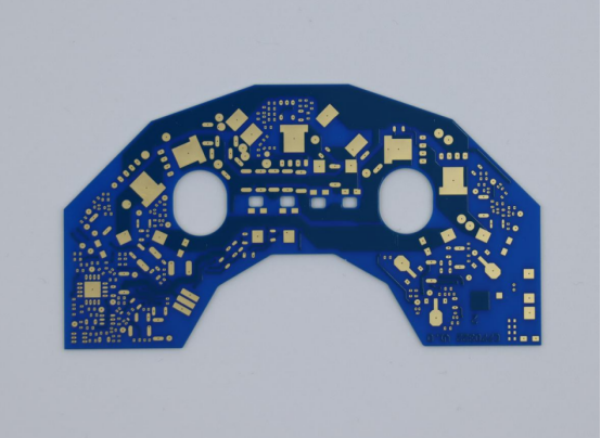
High-density interconnect (HDI) boards and advanced PCB manufacturing demand precision, where even the smallest imperfections can cause significant problems. Excessive hole depressions, a common defect following copper or resin hole filling processes, are one such issue. These depressions create uneven surfaces that can jeopardize electrical performance, assembly quality, and long-term reliability. As technology continues to shrink device sizes, knowing when and why hole filling is essential becomes critical. Whether it’s ensuring smooth signal transmission or improving heat dissipation, mastering the hole filling process is key to building high-performance, reliable products.
What is Excessive Hole Depressions?
Definition and Basic Concepts
Excessive hole depressions refer to a situation in PCB manufacturing where the hole filling process (either resin or copper plating) results in a depression or pit on the surface of the hole. This typically occurs after the hole is filled with copper or resin to create a solid surface for further processing. There are two main types of hole depressions:
l Resin depressions: Caused by the resin material used in the filling process shrinking during curing, leaving a void or depression.
l Copper depressions: These occur when the copper electroplating process is too fast, leading to uneven filling, and creating an indentation.
The difference between the depression and the copper surface can lead to uneven surfaces, impacting the overall performance of the PCB. Ideally, the hole should be filled evenly, creating a smooth, flat surface, but when depressions form, it can create gaps in the surface that affect both the functionality and reliability of the PCB.
Excessive Hole Depressions: Quality Risks
1. Impact on Circuit Pattern and Laser Imaging
Excessive hole depressions can create major problems during the laser imaging process. The depression prevents proper focusing of the laser, causing distortions in the pattern transfer. This issue is especially critical when using Laser Direct Imaging (LDI), where precision is key for creating fine circuit patterns. The result is a misalignment of the electrical traces or holes, potentially leading to short circuits or open circuits in the PCB.
Example: In a high-density PCB, a small depression could misalign a tiny circuit, rendering a section of the board completely unusable.
2. Impact on Soldering and Assembly
Depressions can also cause serious problems during the soldering process. During PCB assembly, solder paste is applied to the pads, and components are placed on top for reflow soldering. If there is a depression where a component is supposed to sit, the surface area for the solder joint is reduced. This leads to poor soldering, potentially causing cold joints, voids, or weak connections.
For example, tiny components like 0201 (0.02 × 0.01 inches) resistors are very sensitive to small defects. If a depression exists on the pad, it might cause solder bridges or insufficient soldering, which can lead to component failure or board malfunction.
3. Risk of Delamination and Mechanical Failure
Large depressions can also introduce stress concentrations in the PCB. When subjected to temperature cycling or mechanical stress, these areas are more prone to delamination—where the layers of the PCB begin to separate. This failure can lead to long-term reliability issues, especially in high-end electronics where performance over time is crucial.
When is Hole Filling Process Necessary?
The hole filling process is a critical step in PCB manufacturing, especially in designs that require high precision and performance. But when exactly is it necessary? Hole filling becomes essential in various situations, such as when dealing with high-density interconnects, ensuring signal integrity, improving heat dissipation, or meeting strict packaging requirements. Whether it’s about enhancing assembly yield, achieving flat surfaces for IC substrates, or providing better electrical conductivity for high-current applications, filling holes ensures that the PCB performs optimally.
Via in Pad (VIP) Design
What is VIP design?
A Via in Pad (VIP) design refers to placing a via (hole for electrical connection) directly on the surface of a pad (the metal area where components are soldered). This design is commonly used in high-density interconnect (HDI) PCBs, where space for routing traces is limited. By placing vias on the pads, designers can maximize available space and ensure effective signal paths between different layers.
How hole filling improves assembly yield in high-density routing:
VIP designs often require hole filling with copper or resin to ensure the surface is flat. Without filling, the via might cause problems during component assembly, such as poor solder joints or component misplacement. Filling the hole ensures a uniform pad surface, improving the assembly yield by preventing solder defects like cold joints or solder bridges, especially in small, high-density components.
Any Layer HDI (High-Density Interconnect)
Importance of high-density interconnect in multi-layer PCBs:
In modern PCB designs, high-density interconnect (HDI) allows for multi-layered connections in a small footprint. HDI technology enables compact, high-performance designs by stacking multiple layers of circuitry. The goal is to create multiple electrical connections between layers using vias, while maintaining a small board size and high reliability.
How hole filling enables Any Layer Interconnects:
In HDI boards, hole filling is essential to create a flat, solid surface for each layer. This is particularly important in Any Layer HDI designs, where vias in any layer may need to be filled to provide a uniform surface for subsequent layers of the PCB. Without proper hole filling, the vias may be uneven, leading to misalignment or signal integrity issues during the layering process. By filling holes with copper, manufacturers can seamlessly stack layers, ensuring the board’s functionality and reliability.
IC Substrate (Package Substrate) Hole Filling Requirements
Flatness requirement for package substrates:
In IC substrates, especially in chip packaging, flatness is crucial. The substrate needs to have a smooth, level surface for precise placement of fine pitch components. Any deviation or unevenness can result in poor solder joints and affect the performance of the final product.
Role of hole filling in heat dissipation for chips:
Hole filling plays a vital role in heat management in IC substrates. Solid copper filling within holes helps improve the thermal conductivity of the PCB, allowing for more efficient heat transfer away from the chip. This is especially important in high-power applications where excess heat can degrade the performance and reliability of chips. Solid copper-filled vias provide a direct path for heat to dissipate, keeping the chip cool during operation.
High Current and High Thermal Conductivity Requirements
How hole filling improves electrical conductivity and heat dissipation:
For applications requiring high current or effective heat dissipation, traditional through-hole vias may not be sufficient. Copper-filled vias offer a solid connection that can handle much higher currents compared to regular plated-through holes (PTH). Filled vias provide a low-resistance path for current, reducing the risk of overheating and electrical losses.
Advantages of electroplated hole filling over regular holes:
Electroplated hole filling creates a uniform copper structure throughout the via, as opposed to regular holes where the copper only coats the hole walls. This solid copper core enhances both the electrical conductivity and thermal performance of the PCB. In comparison, traditional vias often struggle to handle the same electrical or thermal load, making filled vias the preferred option in high-performance electronics like power supplies or LED drivers.
Signal Integrity and Reflection Reduction
How hole filling eliminates "antenna effects" in signal transmission:
In high-speed, high-frequency designs, signal integrity is critical. One common issue in PCBs is the "antenna effect", where open vias or empty holes can act like antennas, causing signal reflection and loss. By filling the vias with copper, the via becomes solid, preventing this unwanted behavior. The filled hole ensures that signals pass through the via without being distorted, maintaining the integrity of high-speed data transmission.
Improved performance for high-frequency signal transmission:
Filling vias with copper also helps to shield signals from interference, improving the performance of high-frequency signal transmission. This is especially beneficial for RF (radio frequency) circuits and other sensitive applications where even minor disruptions in signal flow can result in significant performance degradation.
Air-tight Packaging Requirements
Applications in military and aerospace industries:
In industries like military and aerospace, PCBs must meet strict sealing requirements to ensure air-tight packaging. Any holes or voids in the PCB can lead to air leakage, compromising the device's integrity, especially in vacuum-sealed or pressure-sensitive environments.
How hole filling ensures airtightness:
Filled holes provide a solid structure that prevents the accumulation of gases or moisture in the vias, which could otherwise escape into the environment, especially under high pressure or in vacuum. In military or aerospace applications, this solid structure is crucial to maintaining the performance and safety of the devices. By using copper or resin to fill vias, manufacturers can ensure that the device is completely sealed, enhancing its reliability and longevity.
What Causes Excessive Hole Depressions?
Excessive hole depressions in PCBs are a common issue that can severely impact the quality and performance of electronic devices. These depressions, often caused by uneven filling processes, can arise at various stages of PCB manufacturing. Whether it’s the electroplating or resin filling process, material inconsistencies, or surface preparation issues, each step plays a crucial role in determining the final result. Understanding the root causes of these depressions is key to preventing defects that affect signal integrity, soldering quality, and long-term reliability.
Issues in Electroplated Hole Filling Process
Imbalance in Electroplating Brighteners and Leveling Agents:
In the electroplating process used for hole filling, brighteners and leveling agents are essential to achieve smooth, even copper deposition. However, if the balance between these two chemicals is off, it can lead to uneven plating. This imbalance causes a higher copper buildup around the hole’s edges and a depression in the center of the hole, as the copper doesn’t plate evenly across the entire surface. This results in uneven hole filling, leading to surface defects.
Example: If the brightener is too strong, it may cause the edges of the hole to fill too quickly, while the center lags behind, forming a depression.
Improper Current Density and Pulse Plating Parameters:
Another cause of excessive hole depression is the current density used during electroplating. If the current is too high, it leads to faster deposition of copper at the edges of the hole, while the center does not fill properly, causing copper thinning in the middle. Similarly, improper settings of pulse electroplating parameters can cause the copper to fill too quickly at certain points, forming an uneven surface. These irregularities result in visible depressions or pits.
Example: When plating through holes in a multi-layer PCB, an incorrect current density might cause the outer layer to fill too fast, leaving an unfilled gap at the center, which leads to a depression.
Problems in Resin Hole Filling Process
Viscosity, Flowability, and Shrinkage Rate of Resin Paste:
In the resin hole filling process, the viscosity and flowability of the resin are critical factors in achieving an even fill. If the resin is too thick (high viscosity), it may not flow smoothly into the hole, leaving gaps or uneven fill. On the other hand, if the resin is too thin, it may overflow or create incomplete fills, resulting in depressions. Additionally, when the resin cures, it may shrink too much, leading to a resin depression after hardening.
Example: In a scenario where the resin has high viscosity, it might not fully penetrate the hole, causing voids or uneven coverage. After curing, the shrinkage can deepen the depression further.
Improper Silk Screen Parameters Resulting in Incomplete Fill:
The silk screen process used to apply resin to holes must be precise. If the squeegee pressure is too low, or the speed of the screen print is inconsistent, it can lead to insufficient resin filling in certain areas of the hole. This incomplete fill results in uneven surfaces, which, when cured, form depressions. Proper adjustments to the printing process can help ensure a uniform fill.
Example: If the squeegee pressure is too low, the resin paste might not be fully pushed into the holes, leading to voids or depressions in the cured resin.
Material and Incoming Material Issues
Excessive Resin Flow and Insufficient Prepreg Resin Content:
The material properties of the PCB’s base substrate and resin are crucial in hole filling. If too much resin flow occurs, it can flood the hole, creating an imbalance that leads to a depression. Similarly, if the resin content in the prepreg (partially cured material) is insufficient, it may not provide enough material to fill the hole adequately, causing an incomplete fill and a depression. Both issues can lead to significant defects in the final PCB.
Example: In a case where the resin flow is too high, the hole may fill quickly, but the material may not settle evenly, leaving behind a depression after curing. On the other hand, low resin content can lead to poor fill quality.
Drill Burrs and Rough Hole Walls Impacting Hole Filling:
Drill burrs (small fragments left after drilling) or rough hole walls can significantly affect how well the hole fills with copper or resin. These imperfections prevent the filling material from adhering properly to the surface of the hole. When the material doesn’t adhere evenly, it creates voids or depressions. Additionally, the roughness of the hole wall may cause the filling material to settle unevenly, leading to further depressions.
Example: If a drill leaves burrs inside the hole, the copper filling may not bond properly to the hole’s surface, resulting in poor hole filling and, eventually, a depression in the center.
Pre-treatment and Board Surface Conditions
Oil, Oxide Layer, and Their Effect on Plating Adhesion:
Before the hole filling process begins, the PCB surface needs to be clean and free of any oil or oxide layers. These contaminants can interfere with the adhesion of copper or resin to the hole walls, leading to uneven plating or filling. If there is oil residue or an oxidized layer, it can cause poor adhesion, which results in gaps or depressions in the filled hole. Proper cleaning and surface preparation are essential to avoid these issues.
Example: If the PCB surface is not cleaned properly, the resin or copper might not bond uniformly, leading to defective fills and surface depressions.
Residue from Dry Film Development Affecting Plating Quality:
The dry film used in the PCB process needs to be properly developed before the plating begins. If residual film remains after the development process, it can block or hinder the electroplating or resin filling process, leading to defective fills and depressions. These residuals create obstacles to a smooth fill, resulting in uneven copper or resin deposition.
Example: In a poorly developed dry film, leftover material can prevent proper filling of holes, leading to voids and depressions after plating or curing.
How to Avoid Excessive Hole Depressions?
Excessive hole depressions can lead to serious issues in PCB quality, affecting everything from signal integrity to assembly reliability. Fortunately, these defects can be avoided by making adjustments at key stages of the manufacturing process. Whether it’s fine-tuning the electroplating parameters, optimizing the resin filling process, or selecting the right materials, there are several effective ways to ensure smooth, even hole fills.
Improving Electroplating Process Parameters
How can electroplating parameters be adjusted to avoid hole depressions?
To prevent hole depressions in the electroplating process, it’s crucial to control the plating parameters carefully. A common cause of depressions is uneven copper deposition, where the edges of the hole fill faster than the center. By adjusting plating speed and current density, you can ensure a more uniform deposition of copper across the hole, reducing the likelihood of depressions.
Adjusting Pulse Plating and Current Density:
In electroplating, pulse plating is often used to achieve better control over the plating process. By adjusting the pulse frequency and duty cycle, manufacturers can create a more consistent copper layer inside the hole. Additionally, controlling the current density ensures that the copper fills the hole evenly, preventing the formation of depressions at the center. Both adjustments lead to a smoother surface and better overall hole filling.
Example: If a PCB manufacturer notices consistent depressions, they might reduce the current density or optimize the pulse plating parameters to ensure that the copper fills evenly.
Optimizing Resin Filling Process
How can resin filling be optimized to avoid depressions?
To avoid depressions in resin-filled holes, resin viscosity and flowability are key factors. If the resin is too thick, it may not flow properly into the hole, leading to incomplete filling and depressions. By improving the viscosity control, the resin can be made to flow evenly and fill the hole completely, creating a smooth surface.
Optimizing Silk Screen Process and Squeegee Pressure:
In the silk screen process used for applying resin, squeegee pressure and speed are critical. If the pressure is too low or the speed is inconsistent, the resin may not be applied uniformly, leading to poor fill quality. Adjusting these parameters ensures that the resin is evenly distributed, filling the hole without gaps. By increasing the squeegee pressure or slowing down the application, manufacturers can ensure that the hole is filled thoroughly, reducing the chance of depressions.
Example: A manufacturer can monitor the squeegee pressure and adjust it to ensure the resin fully enters the hole, eliminating voids that could cause depressions.
Material Selection and Process Control
How can material choice help avoid hole depressions?
Selecting the right base materials and resins is essential for minimizing the formation of hole depressions. If the material used has inconsistent properties, it may cause uneven hole filling. For example, using prepreg materials with the right resin content ensures that there is enough material to fill the hole properly, preventing any shrinkage or gaps during the curing process.
Controlling Drilling Quality and Hole Wall Condition:
The quality of the drilling process also plays a major role in preventing depressions. If the hole walls are rough or have drill burrs, it will be harder for the filling material (copper or resin) to adhere evenly. By ensuring that the drill quality is high and the hole walls are smooth, manufacturers can improve the adhesion of the filling material, resulting in a more even fill. Proper hole cleaning before the filling process also helps in achieving a smoother finish.
Example: Before filling a hole with resin or copper, ensuring that the hole is drilled cleanly without burrs helps the filling material spread evenly, preventing uneven surfaces or depressions.
What Are the Impacts of Hole Depressions on Subsequent Manufacturing Processes?
Hole depressions in PCBs may seem like a minor flaw, but they can have significant consequences throughout the entire manufacturing process. From laser imaging distortions to soldering issues and long-term reliability risks, these depressions affect the board’s overall performance and durability. In this section, we’ll explore the various ways hole depressions can disrupt key stages of production, leading to potential failures in electrical conductivity, assembly quality, and product longevity.
Impact on Routing and Laser Imaging
How do hole depressions affect laser imaging and circuit pattern distortion?
Excessive hole depressions can significantly impact the laser imaging process used to transfer circuit patterns onto the PCB. During Laser Direct Imaging (LDI), the laser needs to focus precisely on the surface to create accurate circuit patterns. A depression in the hole creates an uneven surface, which can cause the laser to lose focus, leading to distorted circuit patterns. This misalignment can result in misplaced vias or faulty traces, which can compromise the PCB's functionality.
How do deep depressions cause open circuits or short circuits?
When a hole depression is too deep, it affects the circuit integrity by making it difficult to maintain consistent copper plating. This can lead to areas where the copper layer is too thin, increasing the risk of open circuits (where the electrical connection is lost) or short circuits (where unintended connections form). These issues are particularly problematic during the etching process, where traces are defined, and any uneven copper thickness can lead to errors in the final circuit.
Example: A depression in a via could cause the laser to misalign a small circuit trace, leading to an electrical path that doesn’t connect properly.
Risk to Soldering and Assembly
How do depressions lead to bubbles and solder ball formation during the soldering process?
In the soldering process, a depression can trap gases or volatile materials. When the PCB is heated during reflow soldering, these trapped gases can expand, creating bubbles or solder balls. These bubbles can interfere with the proper flow of solder, leading to weak or unreliable connections, which may cause the solder joint to fail later.
How do depressions affect tiny components and cause tombstoning or cold solder joints?
When assembling small components like 0201 resistors, a depression in the hole or pad can lead to improper solder joint formation. The uneven surface can reduce the contact area between the component and the pad, which can cause tombstoning (where the component lifts off the pad) or cold solder joints (where the solder joint is weak or incomplete). These assembly issues can result in failure or malfunction of the final product.
Example: During PCB assembly, if a depression exists in the pad for a tiny resistor, it may not have enough surface contact for the solder to form a reliable connection, leading to a weak joint that could fail during use.
Impact on Electrical Performance
How do depressions affect conductivity, resistance, and signal transmission?
Hole depressions reduce the effective conductive area in the PCB. This causes increased resistance in the affected area, which can lead to power loss and heat generation, especially in high-current applications. These changes in resistance can affect the signal quality, making the board less efficient at transmitting electrical signals.
How do depressions lead to signal reflection and loss in high-frequency signals?
For high-frequency signals, any depression in the PCB can create an impedance mismatch, which leads to signal reflection. Reflected signals cause signal loss, resulting in degraded performance, especially in high-speed or RF circuits. The depression can act like an unintended "antenna," disrupting the proper flow of signals and leading to data corruption or reduced signal strength.
Example: In a PCB designed for high-speed communication, a depression near a signal trace can create signal reflection, causing data loss or errors in the transmission.
Challenges in Reliability Testing
How do depressions cause stress concentration and cracks in the PCB?
Depressions in PCBs create localized stress points, which can become weak spots under thermal or mechanical stress. Over time, these weak points can cause cracking or delamination, especially during temperature cycling or vibration testing. As the PCB expands and contracts with temperature changes, the depression areas are more likely to fail, leading to cracks that affect the board’s reliability.
How do temperature cycling and vibration affect depressed areas?
During temperature cycling (repeated heating and cooling) or vibration testing, areas with depressions are subjected to greater stress. These stress concentrations can cause fatigue failure, leading to cracks or delamination over time. In mission-critical applications such as aerospace or automotive electronics, these failures can be catastrophic, compromising the safety and functionality of the device.
Example: In a high-reliability application, such as a aerospace PCB, a depression near a via could lead to cracks in the PCB when exposed to the thermal expansion and contraction of constant temperature changes.
How to Assess Hole Filling Quality and Depression Risks?
Assessing the quality of hole filling and identifying potential depression risks are crucial steps in ensuring the performance and reliability of a PCB. Even minor defects in the hole filling process can lead to significant issues in subsequent manufacturing stages, such as misaligned circuits, poor solder joints, or compromised electrical performance. In this section, we will explore effective methods for evaluating hole filling quality, from surface flatness checks to assessing electroplating quality and soldering outcomes.
Surface Flatness Check After Hole Filling
How to check the surface flatness after hole filling?
To ensure the quality of hole filling and to assess potential depression risks, it is crucial to check the surface flatness. An uneven surface can lead to various problems later in the manufacturing process, such as poor soldering or circuit misalignment.
Using Microscopes and Laser Scanning for Surface Flatness:
One of the most effective ways to evaluate surface flatness is by using a microscope or laser scanning equipment. Microscopes allow for detailed visual inspections of the hole's surface, helping to identify minor depressions or irregularities that could affect the overall PCB quality. Laser scanning, on the other hand, uses laser beams to measure the surface profile and detect any deviations from the desired flatness with high precision.
By performing these checks, manufacturers can detect even subtle depressions that might not be visible to the naked eye but could lead to long-term performance issues. This step ensures that the surface is even and smooth before proceeding to the next stage of production.
Example: A laser scan can reveal that a small, invisible depression exists in a via, which would otherwise disrupt the laser imaging or soldering process down the line.
Evaluating Electroplating Quality and Copper Layer Thickness
How to check electroplating quality and copper layer thickness?
The electroplating process is vital for ensuring solid, reliable hole fills, but its effectiveness can vary. Incomplete or uneven plating can lead to depressions or weak spots in the finished PCB.
Checking for Uniform Copper Layer Thickness and Smooth Hole Edges:
The first step in evaluating electroplating quality is to measure the copper layer thickness in and around the hole. This can be done using a thickness gauge or X-ray inspection. The copper should be evenly deposited around the entire hole to ensure the electrical connection remains intact and the hole is properly filled.
It’s also important to inspect the edges of the hole. Uneven copper plating can cause the edges to be rough or raised, potentially leading to issues in soldering or signal integrity. A smooth, consistent copper layer ensures that the hole fill is both effective and long-lasting.
Example: A copper layer thickness measurement might reveal that the hole has a thin layer of copper on one side, leading to the risk of an open circuit.
Soldering and Assembly Testing
How to assess soldering and assembly quality?
After hole filling, it is critical to test how well the filled holes perform during soldering and assembly. Poor hole fills can result in weak or unreliable solder joints, causing functional failures or poor mechanical connections.
Soldering Process Testing and Defect Inspection:
During the soldering process, manufacturers can test the filled holes by inspecting the quality of the solder joints. If the hole fill is not uniform, the solder may not adhere properly, leading to cold solder joints, solder bridges, or insufficient soldering. Inspecting the finished product after soldering can identify areas where the depression in the hole caused defects.
Example: After soldering a component to a pad with a filled hole, you might notice that the solder joint is weak or incomplete, which could be caused by an uneven hole fill, resulting in poor electrical contact.
Conclusion
Ensuring the quality of hole filling and minimizing depression risks are crucial for maintaining the integrity and performance of your PCBs. From laser imaging to soldering and electrical performance, each stage requires precise hole filling to avoid defects that could compromise the final product. By carefully evaluating electroplating quality, surface flatness, and assembly testing, manufacturers can ensure reliable, high-performing boards.
As a trusted name in the PCB industry, PCBMASTER specializes in providing high-quality PCBs with precise hole filling techniques and stringent quality control. With extensive experience in addressing challenges such as hole depressions and surface irregularities, PCBMASTER ensures your boards are ready for even the most demanding applications. Trust us to deliver flawless PCBs that meet your design specifications and exceed your expectations, every time.
FAQs
How Does Excessive Hole Depression Affect PCB Electrical Performance?
Excessive hole depression can have a significant impact on the electrical performance of a PCB. When a hole depression occurs, it can lead to reduced conductive area, increasing resistance at the hole’s surface. This increase in resistance can cause power losses, particularly in high-current applications, where the PCB needs to carry significant electrical loads. Additionally, the signal integrity of the PCB can be compromised, especially in high-speed or high-frequency circuits. Depressions in the hole can cause impedance mismatches, leading to signal reflections, loss of data, and reduced signal strength. For high-frequency circuits, these issues can result in signal degradation and can severely affect the PCB’s performance in sensitive electronic applications.
When Is Hole Filling Process Necessary?
The hole filling process is crucial in specific PCB designs where regular hole processing doesn’t meet the required standards for electrical connectivity, mechanical strength, or signal integrity. Common cases that require hole filling include:
l Via-in-Pad (VIP) Design: In this design, vias are placed directly on the pads, which makes it difficult to handle the holes in traditional ways. Hole filling ensures better assembly yield and reliable soldering by avoiding solder voids and improving the mechanical bond between the component and the PCB.
l High-Density Interconnect (HDI): In high-density designs, especially in Any Layer HDI designs, it is necessary to fill vias with copper to ensure electrical connectivity across multiple layers of the PCB. This process helps create a flat surface for next-layer drilling.
l IC Substrate (Packaging): In semiconductor packaging, a flat, uniform surface is required for precise chip placement and optimal heat dissipation. The filled vias ensure the necessary thermal management and electrical performance.
What Are the Risks of Hole Depressions in the Soldering Process?
Excessive hole depressions can introduce several risks during soldering and assembly:
l Bubble Formation and Solder Balls: A depression in the hole can trap air or volatile substances during the reflow soldering process. When the PCB is heated, these trapped gases expand, creating bubbles or solder balls. These bubbles can interfere with the soldering process, leading to poor joint formation, short circuits, or cold solder joints.
l Soldering Defects and Weak Joints: The depression can affect the surface area available for soldering, resulting in incomplete solder joints or cold soldering. This leads to weak connections that can fail under stress or over time, especially for small components like 0201 resistors or fine-pitch ICs.
l Tombstoning: For small components, a depression on the pad can cause tombstoning, where the component lifts off one side of the pad due to uneven heat distribution during soldering. This can cause functional failures in the assembled PCB.
How to Optimize Electroplating Process to Avoid Excessive Depression?
To prevent excessive hole depression during the electroplating process, manufacturers should focus on optimizing plating parameters and chemical formulations:
l Controlling Plating Parameters: Maintaining consistent plating parameters, such as voltage and current density, ensures that the copper is deposited evenly inside the hole. Too high a current density can cause faster deposition at the edges, resulting in a depression at the center.
l Adjusting Pulse Electroplating: Pulse electroplating allows more controlled deposition. By optimizing pulse frequency and duty cycle, manufacturers can reduce uneven deposition and prevent excessive hole depression.
l Using Proper Brighteners and Leveling Agents: The use of appropriate brighteners and leveling agents ensures smooth copper plating on both the hole's edges and the center. A proper balance between these chemicals helps avoid the creation of depressions or voids in the fill.
By carefully controlling these parameters, manufacturers can achieve an even copper fill and avoid the formation of depressions, which can affect the performance and reliability of the PCB.
How to Assess Hole Filling Quality to Avoid Future Issues?
Assessing the quality of the hole fill is crucial for ensuring that there are no issues in the later stages of PCB manufacturing. Here’s how to evaluate the hole filling quality:
l Microscopic Surface Inspection: Using a microscope allows for detailed inspection of the hole surface. A smooth, flat surface indicates proper filling, while a rough or depressed surface suggests a problem. Inspecting the surface ensures that the hole is filled completely, preventing issues during subsequent processes like soldering and etching.
l Copper Layer Thickness Measurement: After the electroplating process, it's essential to measure the copper layer thickness around the hole. A uniform copper layer ensures that the hole is filled evenly, while significant thickness variation could indicate incomplete filling or areas with high depression risk.
l Soldering and Assembly Testing: Perform soldering tests to assess the quality of the fill. Inconsistent hole fills can lead to weak solder joints or cold solder joints, which can be detected during these tests. Visual inspections of the soldering quality and automated testing for electrical continuity can help ensure the hole fill is reliable.
Author Bio
Hi, I'm Carol, the Overseas Marketing Manager at PCBMASTER, where I focus on expanding international markets and researching PCB and PCBA solutions. Since 2020, I've been deeply involved in helping our company collaborate with global clients, addressing their technical and production needs in the PCB and PCBA sectors. Over these years, I've gained extensive experience and developed a deeper understanding of industry trends, challenges, and technological innovations.
Outside of work, I'm passionate about writing and enjoy sharing industry insights, market developments, and practical tips through my blog. I hope my posts can help you better understand the PCB and PCBA industries and maybe even offer some valuable takeaways. Of course, if you have any thoughts or questions, feel free to leave a comment below—I'd love to hear from you and discuss further!
By carefully evaluating these factors, manufacturers can prevent later-stage issues and ensure the PCB meets both electrical performance and assembly reliability standards.

