







PCB Laser Drilling Process Explained: HDI Microvia Technology, Workflow & Quality Control
As smartphones, wearable devices, AI servers, and 5G communication products continue to become smaller and faster, PCB designs are placing increasingly demanding requirements on microvias. These tiny holes must not only achieve extremely small diameters, but also provide highly accurate interlayer connections. As a result, traditional mechanical drilling can no longer meet the needs of modern HDI PCB manufacturing. PCB laser drilling technology solves this challenge by using high-energy laser beams to create microvias typically smaller than 100μm in diameter.
Compared with conventional mechanical drilling, laser drilling delivers much higher machining precision, better positional accuracy, and the ability to form blind vias without damaging inner circuit layers. These advantages allow HDI PCBs to achieve higher routing density, improved signal integrity, and more reliable electrical connections in compact electronic designs. For this reason, laser microvia technology has become one of the most critical processes in advanced PCB manufacturing.
At PCBMASTER, laser drilling is viewed as a complete process control system rather than a standalone machining step. Factors such as copper window design, laser type selection, drilling parameter optimization, desmear quality, and via wall metallization all directly affect the reliability of the final PCB product.
So, how does PCB laser drilling actually work? Why are HDI boards so dependent on microvia technology? And how do different laser drilling methods influence PCB performance and manufacturing quality? In the following sections, we will explore each of these topics in detail.
What Is the Core Principle of PCB Laser Drilling?
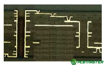
PCB laser drilling uses a high-energy laser beam to remove material from a printed circuit board and create very small holes called microvias. The laser focuses heat onto a tiny area, causing the resin, copper, or other material to melt or vaporize instantly. This process is much more precise than traditional mechanical drilling, especially for HDI PCB manufacturing.
At PCBMASTER, laser drilling is widely used for HDI boards, smartphone PCBs, communication modules, and high-density multilayer designs where small via size and accurate layer connection are critical.
How Does a Laser Remove PCB Material to Form Microvias?
A PCB laser drilling machine focuses laser energy onto a very small point on the board surface. When the energy hits the material, the temperature rises extremely fast. The material then melts, burns away, or turns into gas, creating a micro hole.
Different materials react differently during laser ablation:
l Resin layers vaporize easily
l Copper reflects some laser energy
l Glass fiber requires higher energy to remove
For example:
l A CO₂ laser is very effective for removing FR-4 resin.
l A UV laser can directly remove copper because copper absorbs UV light better.
In HDI PCB production, the laser follows programmed X/Y coordinates to drill thousands of microvias with high positioning accuracy. Typical laser-drilled via sizes range from 25μm to 100μm.
At PCBMASTER, CCD alignment systems and automatic laser calibration help ensure stable microvia positioning during mass production.
What Is the Relationship Between Laser Energy, Pulse Width, and Hole Quality?
Laser energy and pulse width directly affect microvia quality, hole shape, and wall cleanliness.
Higher laser energy removes material faster, but excessive energy can damage the hole wall or burn the copper pad underneath. Low energy may leave resin residue inside the via.
Pulse width refers to how long each laser pulse lasts:
l Short pulse width = lower heat damage and cleaner holes
l Long pulse width = more heat buildup and rougher walls
For example:
l UV lasers usually use ultra-short pulses to produce cleaner HDI microvias.
l CO₂ lasers often use longer pulses for faster resin removal.
A balanced parameter setup is important for:
l Stable via diameter
l Smooth hole walls
l Reduced carbon residue
l Better copper plating reliability
PCBMASTER engineers optimize laser frequency, pulse energy, and drilling speed based on PCB material type and via size requirements.
Why Do Copper, Resin, and Glass Fiber Absorb Laser Energy Differently?
Different PCB materials absorb laser light at different rates. This is one of the most important factors in PCB laser drilling process control.
| PCB Material | Laser Absorption Characteristics | Processing Performance | Processing Performance | Processing Performance |
| Processing Performance | Copper strongly reflects infrared laser energy, especially CO₂ laser wavelengths. It absorbs UV laser energy much better. | Difficult to drill directly with CO₂ lasers, but easier to process with UV lasers. | Poor drilling efficiency with CO₂ lasers, possible incomplete copper removal. | UV Laser |
| Resin Material | Epoxy resin, ABF, and polyimide absorb CO₂ laser energy very efficiently. | Resin materials vaporize quickly and are easy to remove during drilling. | Excessive energy may cause resin burning or carbon residue. | CO₂ Laser |
| Glass Fiber | Glass fiber absorbs laser energy unevenly compared with resin materials. | More difficult to process and requires stable parameter control. | Glass fiber protrusion, rough hole walls, uneven via quality. | CO₂ + Optimized Parameters / UV Combination |
PCBMASTER adjusts laser parameters differently for FR-4, ABF substrate, and high-speed PCB materials to improve drilling consistency and via reliability.
How Does the Heat Affected Zone (HAZ) Influence Hole Wall Quality?
The Heat Affected Zone (HAZ) is the area around the laser-drilled hole that is damaged by heat during processing.
If the heat is too high, several defects may appear:
l Burned resin
l Carbonized hole walls
l Copper pad damage
l Poor plating adhesion
l Cracked microvias after thermal cycling
A smaller HAZ usually means better microvia quality and higher long-term reliability.
UV laser drilling creates a smaller HAZ because it uses shorter wavelengths and lower thermal impact. This is why UV lasers are preferred for fine-pitch HDI PCB designs.
CO₂ lasers generate more heat but offer faster drilling speed for resin materials.
At PCBMASTER, desmear treatment and plasma cleaning are used after laser drilling to remove carbon residue and improve copper plating adhesion inside the via wall.
How Can Blind Via Depth Be Controlled Accurately?
Precise blind via depth control is critical in HDI PCB manufacturing. The laser must stop exactly at the target copper layer without damaging the next layer.
Several methods are used to achieve accurate depth control.
Focus Position Control
The laser focal point must stay at the correct depth during drilling.
If the focus is too high:
l Energy becomes weak
l Resin removal becomes incomplete
If the focus is too low:
l The bottom copper layer may be over-drilled
l Modern laser drilling machines use automatic focus systems and CCD cameras to maintain drilling accuracy across the entire PCB panel.
Laser Energy Compensation
PCB thickness and material density are not always perfectly uniform. Some areas may absorb more energy than others.
Laser energy compensation automatically adjusts power output during drilling to maintain consistent via depth and diameter.
For example:
l Thicker resin areas may require higher energy
l Thin dielectric layers need lower power to avoid copper damage
PCBMASTER uses real-time parameter adjustment systems to improve blind via consistency during volume production.
Multi-Pulse Drilling Strategy
Instead of using one strong laser shot, many HDI PCB factories use multiple low-energy pulses.
This method removes material layer by layer and provides better control over:
l Via depth
l Hole wall smoothness
l Copper protection
l Heat reduction
For example:
l A single high-energy pulse may burn the via bottom.
l Multiple short pulses create cleaner and more stable microvias.
Multi-pulse laser drilling is especially important for:
l High-layer-count HDI boards
l ABF substrates
l Fine-pitch BGA designs
l Ultra-small blind vias under 50μm
PCBMASTER commonly combines UV laser opening with CO₂ multi-pulse dielectric drilling to achieve stable microvia quality in advanced HDI PCB production.
What Is the Difference Between CO₂ Laser and UV Laser Drilling in PCB Manufacturing?
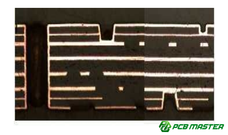
CO₂ lasers are best for fast removal of resin (dielectric materials), while UV lasers are best for high-precision microvias and direct copper processing in HDI PCB manufacturing.
In PCB laser drilling processes, CO₂ and UV lasers are used for different materials and accuracy levels. CO₂ is more efficient for bulk material removal, while UV is used for fine structures like ultra-small microvias under 50μm. At PCBMASTER, both technologies are often combined to achieve stable HDI production performance.
What Are the Characteristics and Applications of CO₂ Laser Drilling?
CO₂ laser drilling is highly efficient for removing organic dielectric materials such as FR-4, PI, and ABF, but it cannot directly process copper layers.
CO₂ laser uses infrared wavelength energy that is strongly absorbed by resin-based materials. This makes it ideal for fast drilling of dielectric layers in HDI PCB manufacturing.
Why CO₂ Laser Works Well on FR-4, PI, and ABF Materials
CO₂ laser energy is easily absorbed by epoxy resin, polyimide (PI), and ABF materials. These materials quickly heat up and vaporize when exposed to CO₂ laser beams.
For example:
l FR-4 boards: fast dielectric layer drilling for standard HDI structures
l PI flexible circuits: efficient via formation in flexible PCB layers
l ABF substrates: commonly used in advanced packaging interconnects
This makes CO₂ laser drilling widely used for dielectric layer removal in HDI PCB laser drilling processes.
Why CO₂ Laser Has Higher Processing Efficiency
CO₂ lasers can deliver higher power output and larger spot energy, which allows faster material removal over large PCB panels.
Key reasons for high efficiency:
l Strong absorption by resin materials
l Larger beam spot for faster coverage
l Suitable for mass production HDI PCB drilling
For example, in smartphone motherboard production, CO₂ lasers are used to rapidly drill thousands of vias per panel in dielectric layers.
PCBMASTER uses CO₂ laser systems for high-volume HDI PCB production where speed and throughput are critical.
Why CO₂ Laser Cannot Directly Process Copper Layers
CO₂ laser operates at infrared wavelength, which copper reflects strongly instead of absorbing.
This leads to:
l Low energy absorption by copper
l Inefficient heating
l No stable ablation of copper material
As a result, CO₂ lasers cannot directly open copper pads. In HDI PCB manufacturing, copper opening must be done by:
l Chemical etching, or
l UV laser pre-ablation
This is why CO₂ laser drilling is always combined with copper opening processes in advanced PCB fabrication.
What Are the Advantages and Applications of UV Laser Drilling?
UV laser drilling is ideal for ultra-fine microvias, high-precision copper processing, and HDI PCB structures requiring minimal heat damage and very small hole sizes.
UV laser uses shorter wavelength energy, which allows higher precision and better absorption by metals like copper.
Why UV Laser Is Suitable for Ultra-Microvia Processing
UV laser has a very small wavelength, which allows:
l Smaller spot size
l Higher precision alignment
l Ability to drill vias below 50μm
For example:
l Smartphone HDI boards
l Wearable devices
l High-density BGA interconnects
UV laser is the preferred solution when PCB designs require ultra-fine microvia laser drilling in HDI PCB manufacturing.
How UV “Cold Processing” Improves Hole Wall Quality
UV laser is often called “cold processing” because it generates less heat compared to CO₂ lasers.
Benefits include:
l Reduced thermal damage (low HAZ)
l Cleaner via walls
l Less carbonization
l Better plating adhesion
For example, in high-speed communication PCBs, UV laser drilling helps reduce signal loss caused by rough via walls and thermal defects.
PCBMASTER applies UV laser technology to improve microvia reliability in high-performance HDI PCB applications.
Why UV Laser Can Directly Ablate Copper Layers
Unlike CO₂ lasers, UV lasers are absorbed much better by copper.
This allows:
l Direct copper opening without chemical etching
l Precise removal of copper pads
l Better control of microvia entrance size
For example:
l Copper pad opening for blind vias
l Fine-pitch HDI structures under BGA chips
This capability makes UV laser essential for advanced HDI PCB laser drilling processes where accuracy is critical.
How to Choose Between CO₂ and UV Laser Drilling?
CO₂ is best for fast dielectric drilling, UV is best for precision copper and microvia formation, and most HDI PCB manufacturing uses a combination of both.
Choosing the right laser depends on material type, via size, and HDI complexity.
How Different Via Sizes Decide Laser Type
l 100–150μm vias → CO₂ laser preferred
l 50–100μm vias → CO₂ + UV hybrid
l <50μm vias → UV laser required
For example:
l Smartphone HDI boards: mostly UV-assisted drilling
l Standard HDI PCB: CO₂ dominant process
How PCB Materials Affect Laser Selection
l FR-4: CO₂ laser for fast dielectric removal
l ABF (Ajinomoto Build-up Film) substrates: UV + CO₂ hybrid for precision packaging
l Polyimide (PI): CO₂ for bulk, UV for fine structures
l High-speed laminates: UV preferred for cleaner via walls
PCBMASTER selects laser systems based on material stack-up and reliability requirements of each customer project.
How HDI Layer Count Affects Laser Process Choice
Higher HDI levels (e.g., HDI 3+ or advanced packaging boards) require:
l Smaller vias
l More precise alignment
l Better thermal control
Lower HDI levels can rely mainly on CO₂ laser drilling.
In advanced multilayer HDI PCB production, UV laser becomes more critical as layer density increases.
CO₂ vs. UV Laser Drilling Comparison Table
| Feature | CO₂ Laser Drilling | UV Laser Drilling |
| Wavelength | Infrared | Ultraviolet |
| Best Material | Resin (FR-4, PI, ABF) | Copper + fine structures |
| Microvia Size | Medium (50–150μm) | Ultra-small (<50μm) |
| Precision | Medium | Very High |
| Thermal Impact | Higher HAZ | Low HAZ |
| Processing Speed | Fast | Slower |
| Copper Processing | Not possible directly | Direct ablation possible |
What Is PCBMASTER’s UV + CO₂ Hybrid Laser Drilling Strategy?
PCBMASTER commonly uses a “UV + CO₂ combined laser drilling process” to balance efficiency and precision.
Process flow:
l UV laser opens copper window
l CO₂ laser removes dielectric layer
l UV laser refines microvia bottom (if needed)
l Post-process desmear and cleaning
Benefits:
l Higher production efficiency
l Better microvia quality
l Stable mass production yield
l Suitable for high-end HDI PCB and advanced packaging boards
This hybrid strategy is widely used in smartphone, automotive electronics, and high-speed communication PCB manufacturing.
Why Is Copper Window Opening Necessary Before PCB Laser Drilling?
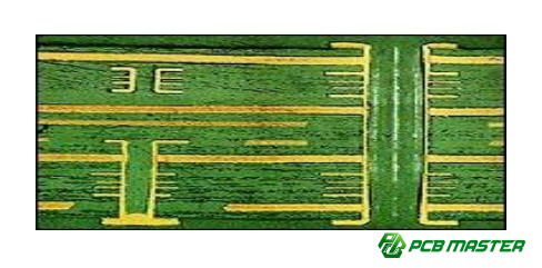
Copper window opening is required to expose or define the copper area so that the laser can accurately drill through dielectric layers or access target layers without damaging surrounding copper.
In PCB laser drilling for HDI boards, copper acts like a barrier. If it is not properly opened or defined, the laser cannot reach the dielectric layer accurately. That is why copper window (Copper Window) preparation is a key pre-process step in HDI PCB manufacturing at PCBMASTER.
What Is a Copper Window in PCB Laser Drilling?
A copper window is a pre-defined opening in the copper layer that exposes the underlying dielectric material for laser drilling.
A copper window (Copper Window) is an area where copper foil is removed or patterned to allow laser access. It defines where the microvia will be formed in HDI PCB structures.
For example:
l In smartphone HDI boards, copper windows define BGA fan-out via locations
l In ABF substrates, copper windows guide ultra-fine microvia positioning
Without copper windows, laser energy would be blocked or scattered by copper layers.
PCBMASTER uses high-precision imaging or UV laser patterning to ensure copper windows match via design requirements exactly.
Why Must CO₂ Laser Drilling Use Copper Window Opening First?
CO₂ lasers cannot efficiently remove copper, so copper must be opened in advance to expose the dielectric layer underneath.
CO₂ laser works well on resin materials but reflects strongly on copper surfaces. If copper is not opened:
l Laser energy cannot penetrate
l Drilling position becomes inaccurate
l Copper may reflect heat and damage nearby areas
For example:
l In FR-4 HDI PCB manufacturing, CO₂ laser is used only after copper is removed via:
l Chemical etching, or
l UV laser ablation
This ensures the CO₂ laser only works on dielectric layers like epoxy resin or ABF.
PCBMASTER follows strict copper window preparation rules to ensure stable CO₂ laser drilling performance in mass production.
How Does Chemical Etching Copper Window Process Work?
Chemical etching removes selected copper areas using photoresist patterning and chemical solutions to form precise copper windows.
Step-by-step process:
1. Apply photoresist layer on copper surface
2. Use photolithography to define via positions
3. Develop and expose copper areas
4. Chemical etching removes unwanted copper
5. Clean and inspect copper window accuracy
For example:
l Used in traditional HDI PCB mass production
l Suitable for FR-4 and standard multilayer boards
Advantages:
l Low cost
l Stable for large-scale production
Limitations:
l Lower precision than UV laser
l Possible undercut issues in fine-pitch designs
PCBMASTER uses chemical etching mainly for standard HDI PCB copper window formation where ultra-fine precision is not required.
How Does UV Laser Copper Window Opening Work?
UV laser directly removes copper with high precision, creating clean and accurate copper windows for microvia drilling.
UV laser uses short wavelength energy that copper can absorb efficiently. This allows direct ablation of copper without chemical processes.
UV copper window process:
l Align PCB using CCD positioning system
l Focus UV laser on copper layer
l Remove copper precisely at target location
l Expose dielectric layer for subsequent drilling
Example use cases:
l Smartphone HDI boards
l Ultra-fine BGA interconnects
l ABF advanced packaging substrates
Advantages:
l Very high precision
l No chemical waste
l Suitable for ultra-small vias (<50μm)
PCBMASTER uses UV laser opening for high-density HDI PCB designs requiring tight tolerance and fine pitch accuracy.
How Does Copper Window Size Affect Via Quality?
Copper window size directly affects via accuracy, hole shape, and plating reliability in HDI PCB laser drilling.
If the copper window is too small:
l Laser may not fully expose dielectric layer
l Via edge becomes irregular
l Poor plating adhesion may occur
If too large:
l Risk of misalignment
l Reduced routing density
l Possible signal integrity issues
Example:
l Smartphone HDI boards use tightly controlled window sizes for BGA fan-out
l Larger boards may allow wider tolerance windows for cost efficiency
PCBMASTER optimizes copper window size based on via diameter, layer stack, and HDI design rules to ensure stable production yield.
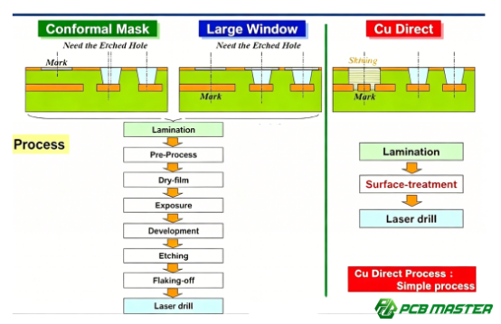
What Are the Differences Between Conformal Mask and Large Window Methods?
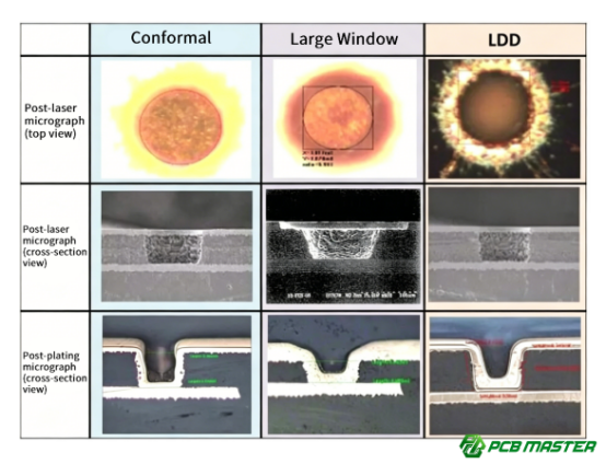
Conformal Mask uses tightly matched copper openings, while Large Window uses oversized openings to improve manufacturing flexibility and HDI design capability.
What Are the Structural Features of Conformal Mask?
Conformal Mask means the copper window closely follows the via shape and size.
Key features:
l Small copper opening margin (50–100μm larger than via)
l High alignment accuracy required
l Suitable for traditional HDI PCB
Example:
l Standard FR-4 HDI boards
l Cost-sensitive applications
Result:
l Good precision
l Slower process control requirements
Where Is Large Window Design Used in HDI PCB?
Large Window uses a much larger copper opening than the via diameter.
Typical use cases:
l Advanced HDI PCB
l High-speed communication boards
l Fine-pitch IC substrate design
Benefits:
l Better alignment tolerance
l Easier laser access
l Supports smaller vias (30–50μm microvias)
How Do These Two Methods Affect Hole Wall Quality?
l Conformal Mask: smoother but slightly rounded via edges
l Large Window: cleaner laser access but requires precise control
For example:
Large Window is commonly used in smartphone HDI boards where ultra-small vias require maximum manufacturing flexibility.
How Do Copper Window Methods Affect Via Accuracy?
l Conformal Mask → higher positional constraint, lower flexibility
l Large Window → higher tolerance, better for fine-pitch designs
However, Large Window requires better process control to avoid misalignment risk.
Conformal Mask vs. Large Window Comparison Table
| Feature | Conformal Mask | Large Window |
| Copper Opening Size | Close to via size | Much larger than via |
| Precision Requirement | High | Medium |
| HDI Level | Standard HDI | Advanced HDI |
| Via Size Capability | Medium (50–100μm) | Ultra-small (30–50μm) |
| Process Flexibility | Lower | Higher |
| Cost | Lower | Higher |
How Does PCBMASTER Choose Copper Window Strategy for Different Boards?
PCBMASTER selects copper window methods based on material type, HDI complexity, and customer design requirements to balance precision, cost, and yield.
PCBMASTER decision logic:
l Standard FR-4 HDI → Conformal Mask + chemical etching
l High-density smartphone PCB → Large Window + UV laser opening
l ABF or advanced packaging → UV laser + precision Large Window design
Selection factors:
l Via diameter requirement
l Layer count (HDI 2, HDI 3+)
l Signal integrity requirements
l Production volume and cost target
By optimizing copper window strategy, PCBMASTER ensures stable HDI PCB laser drilling quality, high yield, and consistent microvia reliability in mass production.
What Are the Standard Process Steps of PCB Laser Drilling?
PCB laser drilling in HDI manufacturing follows five key steps: surface preparation and alignment, laser parameter setup, laser drilling execution, desmear cleaning, and hole metallization.
In HDI PCB laser drilling, each step is critical because microvias are extremely small (often 30–100μm). A small mistake in any stage can affect electrical reliability. At PCBMASTER, the process is tightly controlled to ensure stable microvia quality for smartphone, automotive, and high-speed PCB applications.
Step 1: What Happens During PCB Surface Preparation and Positioning?
This step ensures the PCB surface is clean and accurately aligned so the laser can drill microvias at the correct positions.
Surface preparation and positioning is the foundation of HDI PCB laser drilling accuracy.
Why Is PCB Surface Cleaning Necessary?
Before laser drilling, the PCB surface must be free of dust, oil, and oxidation.
If the surface is not clean:
l Laser energy may scatter
l Via position may shift
l Hole quality becomes unstable
For example, in smartphone HDI boards, even tiny dust particles can cause via misalignment or incomplete drilling.
PCBMASTER uses automated cleaning systems to ensure consistent surface quality before laser processing.
What Is the Role of CCD Vision Positioning System?
CCD visual alignment systems are used to locate exact drilling coordinates.
They help to:
l Detect fiducial marks on PCB
l Correct panel position errors
l Improve microvia placement accuracy
For HDI PCB laser drilling, CCD alignment is essential because layer stacking can slightly shift during lamination.
PCBMASTER uses high-resolution CCD systems to maintain micron-level alignment accuracy in mass production.
Step 2: How Are Laser Parameters Set in PCB Laser Drilling?
Laser parameters such as energy, frequency, spot size, and focus depth are adjusted to control via size, depth, and hole quality.
Correct parameter setup is the key to stable PCB laser drilling quality control.
How Do Laser Energy and Frequency Affect Drilling?
l Higher energy → faster material removal but higher risk of burning
l Lower energy → cleaner holes but slower drilling speed
l Higher frequency → smoother hole edges
l Lower frequency → stronger single pulse impact
For example:
CO₂ lasers often use higher energy for FR-4 resin removal, while UV lasers use controlled low-energy pulses for microvia precision.
How Does Spot Size Affect Via Diameter?
l Laser spot size directly determines microvia diameter.
l Large spot → larger via (100–150μm)
l Small spot → ultra-fine via (<50μm)
In HDI PCB manufacturing, spot size must match the design rule of BGA or IC substrate layout.
PCBMASTER adjusts optical focus systems to match customer via design requirements.
How Does Focus Depth Affect Blind Via Quality?
Focus depth controls where the laser energy is concentrated inside the PCB layer stack.
If focus is incorrect:
l Too shallow → incomplete drilling
l Too deep → damage to lower copper layer
Accurate focus ensures clean blind vias and stable layer-to-layer connectivity in HDI PCB structures.
Step 3: How Does the Laser Drilling Process Actually Work?
Laser drilling removes PCB material using controlled beam patterns such as single pulse, circular scanning, or spiral scanning depending on via type and material.
This is the core stage of HDI PCB laser microvia formation.
What Is Single-Point Laser Drilling?
Single-point drilling uses high-energy pulses to remove material at one fixed spot.
l Fast process
l Suitable for larger vias
l Less precision than scanning methods
Example: used in thicker FR-4 dielectric layers.
What Is Circular (Ring) Scanning Drilling?
Ring scanning moves the laser in a circular path around the via.
Benefits:
l More uniform hole wall
l Better control of via diameter
l Reduced thermal damage
Common in medium-size HDI microvias (50–100μm).
What Is Spiral Scanning Drilling?
Spiral scanning starts from the center and moves outward.
Advantages:
l Very smooth hole walls
l Excellent for ultra-fine vias
l Reduced carbon residue
Used in advanced HDI PCB and IC substrate manufacturing.
How Are Different Drilling Strategies Used in Real Production?
l Single-point → fast drilling, low precision
l Ring scan → balanced quality and speed
l Spiral scan → highest quality microvias
PCBMASTER selects drilling mode based on material type and HDI layer complexity.
Step 4: Why Is Desmear Necessary After Laser Drilling?
Desmear removes carbonized resin and residue inside vias to ensure strong copper adhesion during plating.
Laser drilling leaves behind residue called “smear,” which must be cleaned for reliable PCB interconnection.
Why Must Laser Drilled Holes Be Cleaned?
After laser drilling:
l Resin may be carbonized
l Glass fiber may remain exposed
l Hole wall may be contaminated
If not cleaned:
l Copper plating adhesion becomes weak
l Via reliability decreases
l Electrical failure may occur
How Does High-Permanganate Desmear Work?
High permanganate solution chemically oxidizes and removes resin residue.
Process steps:
1. Swell resin surface
2. Oxidize carbonized material
3. Rinse and neutralize
This method is widely used in FR-4 HDI PCB production.
How Does Plasma Desmear Work?
Plasma cleaning uses ionized gas to remove residue.
Benefits:
l No chemical liquid waste
l Better for fine microvias
l More uniform cleaning
Used in high-end HDI PCB and ABF substrate manufacturing.
Why Are High Aspect Ratio Microvias Hard to Clean?
Deep and narrow vias make chemical penetration difficult.
Problems include:
l Incomplete residue removal
l Uneven hole wall treatment
l Higher risk of plating voids
PCBMASTER uses combined desmear processes for high-aspect-ratio HDI PCB structures.
Step 5: How Does Hole Metallization and Copper Plating Work?
Hole metallization uses chemical copper deposition followed by electroplating to form conductive connections between PCB layers.
This step turns a mechanical hole into an electrical interconnect in HDI PCB structures.
What Is Electroless Copper Deposition?
Electroless copper is a chemical process that deposits a thin copper layer inside the via wall.
Purpose:
l Create conductive seed layer
l Prepare for electroplating
Without this step, electroplating cannot build uniform copper layers.
How Does Electroplating Create Layer-to-Layer Connection?
Electroplating thickens the copper layer inside the via.
It ensures:
l Electrical continuity between layers
l Mechanical strength
l Current-carrying capability
For example:
In smartphone HDI PCBs, via plating must support high-frequency signal transmission.
Why Is Copper Thickness Uniformity Important?
Uneven copper thickness can cause:
l Electrical resistance imbalance
l Thermal stress concentration
l Via cracking during thermal cycling
Uniform copper plating ensures long-term reliability of HDI PCB laser drilled microvias.
PCBMASTER strictly controls plating current density and solution chemistry to ensure consistent via copper quality in mass production.
What Are the Key Process Control Points in PCB Laser Drilling?
The most critical control points in PCB laser drilling are via diameter consistency, position accuracy, blind via depth control, hole wall quality, heat control, and material stability.
In HDI PCB laser drilling processes, microvias are extremely small and sensitive. Even a small deviation in laser energy, alignment, or material behavior can cause defects. At PCBMASTER, process control is treated as the core factor for achieving stable mass production yield.
How Is Via Diameter Consistency Controlled in PCB Laser Drilling?
Via diameter consistency is controlled by stabilizing laser energy, spot size, focus accuracy, and material response during drilling.
Via size in HDI PCB laser drilling depends mainly on laser parameters and material uniformity.
Key control methods:
l Stable laser pulse energy to avoid over-burning
l Fixed optical spot size using calibrated lenses
l Real-time focus correction across PCB panels
l Material thickness compensation during processing
For example:
In smartphone HDI boards, a 10μm variation in via diameter can affect BGA routing reliability.
PCBMASTER uses automated calibration systems to ensure consistent HDI microvia diameter control in PCB laser drilling production.
What Causes Via Position Misalignment in PCB Laser Drilling?
Via offset is mainly caused by PCB warpage, misalignment of fiducial marks, thermal expansion, and machine calibration errors.
Common causes include:
l PCB shrinkage or expansion after lamination
l Incorrect CCD recognition of alignment marks
l Mechanical positioning drift in production equipment
l Thermal deformation during laser processing
For example:
In multilayer HDI PCBs, slight warpage after lamination can shift via positions by several microns.
PCBMASTER uses high-precision CCD alignment and real-time compensation systems to reduce PCB laser drilling via misalignment issues.
Why Do Blind Vias Sometimes Not Reach or Over-Drill?
Blind via depth errors occur when laser energy, focus depth, or material thickness is not properly controlled.
Two main failure types:
Under-drilling (not reaching target layer)
l Insufficient laser energy
l Incorrect focus position
l Material thickness variation
Result: incomplete electrical connection.
Over-drilling (damaging lower layer)
l Excess energy
l Excess pulse count
l Incorrect depth calibration
Result: copper layer damage and reliability failure.
For example:
In HDI PCB manufacturing, blind vias must stop exactly at inner copper layers to ensure proper interconnection.
PCBMASTER applies multi-stage depth control in HDI laser blind via drilling processes.
How Can Hole Wall Roughness and Carbonization Be Improved?
Hole wall quality is improved by optimizing laser energy, using multi-pulse drilling, and applying proper desmear cleaning.
Main causes of poor hole walls:
l Excess laser energy burning resin
l Uneven material absorption
l Incomplete removal of glass fiber
l Poor drilling strategy selection
Improvement methods:
l Use lower energy with multiple pulses
l Apply spiral or ring scanning instead of single shot
l Optimize CO₂ vs UV laser combination
l Improve post-drilling desmear process
For example:
UV laser drilling produces smoother walls compared to CO₂ due to lower heat impact.
PCBMASTER optimizes HDI PCB laser drilling wall quality through controlled energy and scanning strategies.
How Can the Heat Affected Zone (HAZ) Be Reduced in Laser Drilling?
HAZ is reduced by lowering thermal input, using short laser pulses, and selecting UV laser for fine structures.
Heat Affected Zone (HAZ) is the area around the via that is thermally damaged.
Reduction methods:
l Use short pulse width lasers (especially UV laser)
l Reduce single pulse energy
l Use multi-pulse gradual ablation
l Improve cooling and process timing
For example:
UV laser drilling creates much smaller HAZ than CO₂, making it suitable for ultra-fine HDI PCB structures.
PCBMASTER prioritizes low-HAZ processes in high-reliability HDI PCB laser microvia production.
How Does PCB Expansion and Shrinkage Affect Position Accuracy?
PCB material expansion and shrinkage cause alignment errors between laser drilling and target layers, leading to via misplacement.
Causes include:
l Thermal expansion during lamination
l Moisture absorption in resin materials
l Uneven cooling after pressing
l Material property variation across panel
Impact:
l Misaligned vias
l Reduced interconnect reliability
l Signal integrity degradation in high-speed PCBs
Example:
In large PCB panels, thermal expansion can shift coordinates by several microns to tens of microns.
PCBMASTER uses controlled environmental conditioning and compensation algorithms for stable HDI PCB laser drilling alignment accuracy.
How Does PCBMASTER Stabilize Microvia Yield in Mass Production?
PCBMASTER stabilizes microvia yield through strict process control, advanced laser systems, real-time monitoring, and optimized HDI manufacturing parameters.
Key strategies:
l CCD high-precision alignment for every panel
l Automated laser parameter calibration
l Hybrid UV + CO₂ laser process optimization
l Strict desmear and plating process control
l Real-time defect inspection (AOI systems)
For example:
In high-volume smartphone PCB production, PCBMASTER maintains stable microvia yield by continuously adjusting laser parameters based on material batch variation.
This ensures reliable HDI PCB laser drilling mass production quality control, reducing defects such as misalignment, under-drilling, and via roughness.
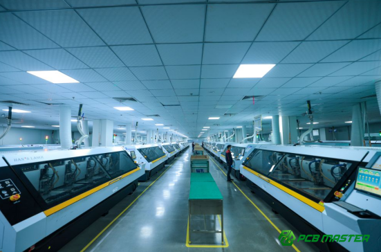
What Are the Common Defects in HDI PCB Laser Drilling and How Can They Be Solved?
The most common HDI PCB laser drilling defects include residual resin (smear), copper damage, via misalignment, inconsistent hole size, copper burrs at the hole entrance, and plating voids. These issues can be solved through optimized laser parameters, copper window design, material selection, and desmear process control.
In HDI PCB laser drilling manufacturing, defects usually come from unstable energy control, incorrect material matching, or poor process integration. At PCBMASTER, defect control is handled at every stage—from laser setup to post-plating—to ensure stable microvia reliability.
What Causes Hole Wall Residual Resin (Smear) in Laser Drilling?
Hole wall residue occurs when laser energy does not fully remove resin or when carbonized material remains after drilling.
Residual resin (also called smear or carbonization) is common in CO₂ laser drilling of FR-4 and ABF materials.
Main causes:
l Insufficient laser energy
l Incomplete vaporization of resin
l Poor scanning pattern selection
l High glass fiber content blocking removal
Impact:
l Weak copper plating adhesion
l High risk of via failure
l Increased electrical resistance
For example:
In smartphone HDI boards, residual smear can cause signal instability in high-speed circuits.
PCBMASTER uses optimized energy profiles and post-desmear cleaning to reduce PCB laser drilled via contamination defects.
Why Does Copper Layer Damage Occur at Via Bottom?
Copper damage happens when laser energy is too high or improperly focused, causing overheating or physical erosion of the target copper layer.
Main causes:
l Excess laser energy
l Incorrect focus depth
l Over-drilling beyond target layer
l Poor energy distribution in UV/CO₂ hybrid systems
Impact:
l Broken electrical connection
l Reduced reliability in multilayer HDI PCB
l Increased failure during thermal cycling
Example:
Over-drilling in HDI PCB can damage inner signal layers, leading to open circuits.
PCBMASTER prevents this by using precise depth control systems in HDI laser blind via drilling processes.
What Causes Microvia Misalignment in PCB Laser Drilling?
Via offset is caused by PCB warpage, alignment errors, thermal expansion, and mechanical positioning drift.
Main causes:
l Lamination shrinkage or expansion
l CCD alignment detection errors
l Panel deformation during heating
l Machine calibration drift
Impact:
l Poor layer-to-layer connectivity
l Reduced routing density
l Signal integrity issues
Example:
In large HDI panels, even a small thermal shift can move via position by several microns.
PCBMASTER uses CCD correction and thermal compensation to maintain high-precision PCB laser drilling alignment accuracy.
Why Do Via Diameters Become Inconsistent?
Inconsistent via size occurs when laser energy, focus, or material absorption is unstable across the PCB panel.
Main causes:
l Fluctuating laser power
l Uneven material thickness
l Incorrect focus calibration
l Different resin absorption rates
Impact:
l Poor BGA routing matching
l Electrical resistance variation
l Reduced yield in HDI PCB production
Example:
In smartphone HDI boards, inconsistent via size can affect high-speed signal routing stability.
PCBMASTER ensures consistent HDI microvia diameter control using automated laser calibration systems.
What Causes Copper Burrs at Via Openings?
Copper burrs occur when copper is not cleanly removed during laser opening, leaving rough edges or partially melted material.
Main causes:
l Incomplete UV laser copper ablation
l Improper etching process
l Excess energy causing copper melting instead of vaporization
Impact:
l Poor plating adhesion
l Increased electrical resistance
l Reduced reliability in fine-pitch designs
Example:
Burrs in BGA areas can interfere with solder joint reliability.
PCBMASTER optimizes copper window opening to ensure smooth edges in HDI PCB laser drilling pre-process steps.
Why Do Plating Voids and Electrical Open Circuits Occur?
Plating voids occur when hole walls are not clean or conductive layers are uneven before copper plating.
Main causes:
l Residual resin or carbon inside vias
l Poor desmear process
l Uneven electroless copper deposition
l Air entrapment in deep microvias
Impact:
l Open circuits between layers
l High resistance connections
l Long-term reliability failure
Example:
In automotive HDI PCB, plating voids can cause serious functional failure.
PCBMASTER ensures plating reliability through strict cleaning and copper deposition control.
How Can Laser Drilling Yield Be Improved Through Process Optimization?
Yield improvement is achieved by optimizing laser parameters, copper window design, material selection, and desmear cleaning processes.
Defect vs. Solution Optimization Table
| Defect Type | Impact | Root Cause | Optimization Solution |
| Residual resin (smear) | Weak copper adhesion, higher via resistance, risk of open circuit in HDI PCB laser drilled vias | Insufficient energy or poor scanning | Optimize laser energy + improve desmear process |
| Copper damage | Broken inner layer connection, electrical failure, reduced multilayer reliability | Over-drilling or wrong focus | Precise depth control + CCD alignment |
| Via misalignment | Poor layer-to-layer registration, routing difficulty, signal integrity degradation | PCB warpage or CCD error | Thermal compensation + alignment correction |
| Uneven via size | BGA mismatch, inconsistent electrical performance, reduced manufacturing yield | Energy instability | Laser calibration + focus optimization |
| Copper burrs | Poor plating adhesion, increased resistance, soldering reliability issues | Improper copper removal | Improve UV laser or etching window control |
| Plating voids | Open circuits, high resistance joints, long-term reliability failure under thermal cycling | Poor cleaning or deposition | Enhance desmear + improve electroless copper process |
How Laser Parameter Optimization Improves Yield
Laser parameters directly affect via quality:
l Energy tuning prevents over-burning
l Frequency control improves edge smoothness
l Pulse adjustment reduces thermal damage
PCBMASTER continuously tunes parameters for each PCB batch to maintain stable HDI PCB laser drilling yield performance.
How Copper Window Design Improves Drilling Quality
Proper copper window design ensures:
l Accurate laser entry point
l Reduced reflection issues
l Better via shape control
Example:
Large Window design is used in advanced HDI PCBs to support ultra-fine vias.
How Material Selection Impacts Defect Rate
Different materials behave differently:
l FR-4 → stable but may generate smear
l ABF → high precision but sensitive
l PI → flexible but harder to control
Choosing the right material reduces laser drilling defects significantly.
How Desmear Optimization Improves Reliability
Desmear process ensures clean via walls before plating.
Key improvements:
l Stronger resin removal
l Better plasma cleaning for fine vias
l Reduced carbon residue
PCBMASTER integrates multi-stage desmear systems to ensure strong copper adhesion in HDI PCB microvia manufacturing.

How Do Different PCB Materials Affect Laser Drilling Processes?
Different PCB materials affect laser drilling speed, accuracy, energy absorption, and defect rate because each material (FR-4, ABF, high-speed laminates, PI, and resin systems) reacts differently to laser energy and heat.
In HDI PCB laser drilling manufacturing, material selection is one of the most important factors. At PCBMASTER, laser parameters are adjusted based on material type to ensure stable microvia quality, low defect rate, and high reliability.
What Are the Laser Drilling Characteristics of FR-4 Material?
FR-4 is easy to process with CO₂ laser because its epoxy resin absorbs infrared energy well, but it may produce more thermal damage and requires strong desmear control.
FR-4 is the most common PCB base material used in standard HDI PCB laser drilling.
Key characteristics:
l Resin layer absorbs CO₂ laser efficiently
l Glass fiber is harder to remove and may cause rough hole walls
l Suitable for medium-size microvias (50–150μm)
l Cost-effective for mass production
Example:
In consumer electronics like routers or TVs, FR-4 HDI boards are widely used due to stable and low-cost laser drilling performance.
PCBMASTER uses optimized CO₂ laser settings and post-desmear cleaning to ensure reliable FR-4 HDI microvia quality.
Why Does ABF Substrate Rely More on UV Laser Drilling?
ABF requires UV laser because it supports ultra-fine vias, high precision, and low thermal damage needed for advanced packaging.
ABF is widely used in IC substrates and advanced HDI PCB structures.
Key reasons:
l Requires ultra-small vias (<50μm)
l Needs extremely high positioning accuracy
l Sensitive to heat damage
l Copper layer opening often required
For example:
In CPU and GPU packaging, ABF substrates use UV laser drilling for dense interconnections.
UV laser advantages for ABF:
l Small spot size
l High precision copper ablation
l Low heat affected zone (HAZ)
PCBMASTER applies UV-based processes for advanced ABF substrate laser microvia drilling.
What Are the Challenges of High-Speed High-Frequency PCB Materials in Laser Drilling?
High-speed materials are difficult to drill because they have low dielectric loss, uneven laser absorption, and stricter requirements for via smoothness.
High-frequency materials include Rogers, Megtron, and other low-loss laminates.
Key challenges:
l Uneven resin composition affects laser absorption
l Strict requirement for smooth via walls
l Signal integrity sensitivity to roughness
l Risk of carbon residue affecting high-speed signals
Example:
In 5G communication PCBs, via wall roughness can directly affect signal loss at high frequencies.
Solutions:
l Use UV laser for cleaner vias
l Optimize multi-pulse drilling
l Improve desmear process to reduce residue
PCBMASTER uses controlled laser profiles for high-frequency PCB laser drilling reliability improvement.
What Are the Key Considerations for PI and Rigid-Flex PCB Laser Drilling?
PI (polyimide) and rigid-flex boards require careful thermal control because they are flexible, heat-sensitive, and prone to deformation during laser processing.
PI material is widely used in flexible circuits and wearable electronics.
Key considerations:
l PI absorbs CO₂ laser well but may carbonize easily
l Flexible structure may deform during drilling
l Requires low-heat, controlled energy processing
l Multi-layer alignment is more difficult
Example:
In wearable smart devices, flexible circuits must maintain stability even after repeated bending.
Best practices:
l Use low-energy multi-pulse CO₂ laser
l Apply UV laser for fine structures when needed
l Control temperature during processing
PCBMASTER applies flexible PCB-specific laser parameters for rigid-flex HDI laser drilling stability.
How Do Different Resin Systems Affect Desmear and Cleaning Processes?
Different resin systems (epoxy, ABF, PI, high-speed laminates) respond differently to desmear processes, affecting cleaning efficiency and plating adhesion.
Resin type determines how easily residue can be removed after laser drilling.
Key differences:
l Epoxy resin → easy to remove with chemical desmear
l ABF → requires controlled plasma cleaning
l PI → more resistant, needs stronger energy or combined methods
l High-speed resin → requires gentle cleaning to avoid damage
Example:
In ABF substrates, plasma desmear is preferred to avoid over-etching fine structures.
PCBMASTER adjusts desmear methods based on material type to ensure clean via walls and strong copper plating adhesion.
Comparison Table: PCB Materials vs Laser Drilling Behavior
PCB Material Laser Compatibility Best Laser Type Key Difficulty Typical Application FR-4 Best for high-volume manufacturing CO₂ laser Glass fiber roughness, thermal damage Consumer electronics, standard HDI PCB ABF substrate Very high precision requirement UV laser Ultra-fine via control (<50μm) CPU/GPU packaging, IC substrates High-speed laminates (Rogers, Megtron) Medium UV + optimized CO₂ Signal integrity sensitivity, low roughness demand 5G, RF communication PCBs PI (polyimide) Medium-high (flexible) CO₂ + UV hybrid Thermal deformation, carbonization risk Flexible PCB, wearables Resin systems (general) Varies by type CO₂ / UV / hybrid Desmear complexity, residue control HDI multilayer boards
| PCB Material | Laser Compatibility | Best Laser Type | Key Difficulty | Typical Application |
| FR-4 | Best for high-volume manufacturing | CO₂ laser | Glass fiber roughness, thermal damage | Consumer electronics, standard HDI PCB |
| ABF substrate | Very high precision requirement | UV laser | Ultra-fine via control (<50μm) | CPU/GPU packaging, IC substrates |
| High-speed laminates (Rogers, Megtron) | Medium | UV + optimized CO₂ | Signal integrity sensitivity, low roughness demand | 5G, RF communication PCBs |
| PI (polyimide) | Medium-high (flexible) | CO₂ + UV hybrid | Thermal deformation, carbonization risk | Flexible PCB, wearables |
| Resin systems (general) | Varies by type | CO₂ / UV / hybrid | Desmear complexity, residue control | HDI multilayer boards |
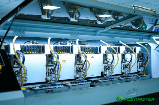
How Does HDI Microvia Processing Affect PCB Electrical Performance and Reliability?
HDI microvia processing directly affects signal speed, impedance stability, interlayer connection strength, routing density, and long-term reliability of the PCB.
In HDI PCB laser drilling and microvia fabrication, the quality of microvias determines whether high-speed signals can pass cleanly between layers. At PCBMASTER, microvia design and laser drilling control are optimized to ensure stable electrical performance for high-speed and high-density applications.
How Do Microvias Affect High-Speed Signal Integrity in PCBs?
Microvias influence signal integrity by controlling impedance, reducing signal loss, and minimizing reflection in high-speed PCB transmission paths.
In high-speed PCB design (such as 5G, servers, and RF boards), signals travel very fast, so even small defects in vias can cause distortion.
Key impacts:
l Rough via walls increase signal loss
l Poor via geometry causes impedance mismatch
l Excessive via length increases delay
For example:
In 5G communication PCBs, poorly formed microvias can reduce signal quality and increase bit error rate.
PCBMASTER uses optimized HDI PCB laser drilling techniques to ensure smooth via walls and stable signal transmission paths.
How Does Via Size Affect Interlayer Connection Reliability?
Smaller and more precise vias improve interlayer connection stability, while inconsistent via size can cause weak or unstable electrical connections.
Via size directly affects:
l Contact area between layers
l Current carrying capacity
l Mechanical strength of the interconnect
If vias are too large or uneven:
l Risk of weak copper plating
l Increased electrical resistance
l Higher probability of failure under stress
Example:
In smartphone HDI boards, consistent 40–60μm microvias are required to ensure reliable layer stacking.
PCBMASTER tightly controls laser microvia diameter consistency in HDI PCB manufacturing to improve reliability.
How Does Copper Thickness Inside Vias Affect Long-Term Reliability?
Proper and uniform copper thickness inside microvias ensures stable electrical performance and prevents cracking or failure during thermal cycling.
Copper plating inside vias provides:
l Electrical conductivity
l Mechanical strength
l Thermal stress resistance
If copper is too thin:
l Via may crack under temperature changes
l Resistance increases over time
If copper is uneven:
l Stress concentration occurs
l Reliability decreases in long-term use
Example:
In automotive electronics, PCB vias must withstand repeated heating and cooling cycles without failure.
PCBMASTER controls electroless copper and electroplating processes to ensure uniform via copper thickness in HDI PCBs.
Why Do Laser Blind Vias Enable High-Density PCB Routing?
Laser blind vias allow connections between specific layers without passing through the entire board, freeing space for denser routing and smaller PCB designs.
Blind vias created by laser drilling only connect selected layers.
Advantages:
l Saves PCB routing space
l Enables smaller board size
l Supports finer pitch BGA components
l Reduces signal path length
For example:
In smartphone motherboards, blind vias allow routing under chips without occupying full board thickness.
PCBMASTER uses UV and CO₂ laser drilling for precise HDI blind via formation to maximize routing density.
Why Are Laser Microvias Essential for Advanced Packaging Substrates?
Advanced packaging substrates require laser microvias because they support ultra-fine pitch interconnects, high I/O density, and extremely small feature sizes that mechanical drilling cannot achieve.
Traditional drilling cannot reach:
l Sub-50μm via sizes
l Ultra-dense interconnection networks
l High-layer stacking accuracy
Laser microvias are essential for:
l AI chips
l High-performance computing (HPC) systems
Example:
ABF substrates in advanced processors use laser microvias to connect thousands of signal paths in a very small area.
PCBMASTER supports advanced IC substrate laser microvia drilling for next-generation semiconductor packaging applications.
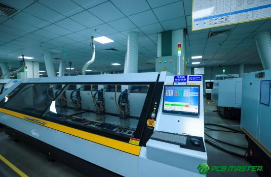
How Does PCBMASTER Ensure Laser Drilling Quality and Stable Delivery?
PCBMASTER ensures stable HDI PCB laser drilling quality and delivery through advanced manufacturing capability, high-precision alignment systems, multi-laser process integration, strict inspection, and engineering optimization support.
In modern HDI PCB laser drilling manufacturing, consistency is more important than single-point accuracy. PCBMASTER focuses on process stability, yield control, and design optimization to support high-volume production for smartphones, automotive electronics, and advanced packaging.
What Is PCBMASTER’s HDI Laser Drilling Manufacturing Capability?
PCBMASTER has advanced HDI PCB laser drilling production capability covering microvia sizes, multilayer structures, and high-density interconnect designs.
PCBMASTER specializes in:
l HDI microvias (as small as 30–100μm)
l Blind via and buried via structures
l High-layer-count PCB stack-ups
l Advanced materials such as FR-4, ABF, and high-speed laminates
For example:
In smartphone motherboard production, PCBMASTER handles dense via arrays used under BGA chips with high precision and repeatability.
This capability ensures stable HDI PCB laser microvia manufacturing for high-density electronic applications.
How Does High-Precision CCD Automatic Alignment Improve Accuracy?
Short answer: CCD automatic alignment improves laser drilling accuracy by detecting reference marks and correcting positional errors in real time.
CCD vision systems are used to:
l Detect fiducial marks on PCB panels
l Correct board position before drilling
l Compensate for warpage or shrinkage
l Improve layer-to-layer alignment accuracy
For example:
If a PCB shifts slightly during lamination, CCD alignment ensures the laser still drills at the correct microvia location.
PCBMASTER uses high-resolution CCD systems to achieve micron-level accuracy in HDI PCB laser drilling alignment control.
Why Is Multi-Laser Equipment Integration Important in HDI Manufacturing?
Short answer: Using multiple laser types (CO₂ + UV) allows PCBMASTER to handle different materials and via requirements more efficiently and precisely.
Different lasers are used for different tasks:
l CO₂ laser → fast dielectric (resin) removal
l UV laser → copper opening and ultra-fine microvias
l Hybrid systems → advanced HDI structures
For example:
In ABF substrate manufacturing, UV laser opens copper while CO₂ laser removes dielectric layers efficiently.
Benefits:
l Higher production flexibility
l Better process optimization
l Improved yield for complex HDI PCB designs
PCBMASTER integrates UV + CO₂ hybrid laser drilling systems for advanced PCB manufacturing efficiency.
How Does PCBMASTER Control Microvia Quality Through Inspection and AOI?
PCBMASTER uses AOI and microvia inspection systems to detect defects such as misalignment, incomplete drilling, and via shape abnormalities.
Quality control includes:
l Optical inspection of via position
l Measurement of via diameter consistency
l Detection of residual resin or carbonization
l Cross-section analysis for plating quality
For example:
In high-volume production, AOI systems automatically reject panels with via defects before plating.
This ensures stable HDI PCB laser drilling defect control and yield improvement.
What DFM Suggestions Does PCBMASTER Provide for Advanced HDI PCB Design?
PCBMASTER provides Design for Manufacturing (DFM) guidance to help customers optimize via size, copper window design, material selection, and stack-up structure.
Key DFM recommendations:
l Avoid overly small via-to-pad ratios
l Optimize copper window size for laser access
l Ensure consistent dielectric thickness
l Match material type with laser capability
For example:
Reducing via density below process capability can significantly increase yield in HDI PCB production.
PCBMASTER supports customers with HDI PCB laser drilling manufacturability optimization before production.
How Does PCBMASTER Help Customers Optimize Microvia Design?
PCBMASTER works with customers to adjust via structure, laser strategy, and material stack-up to improve yield, reliability, and cost efficiency.
Optimization support includes:
l Via size and aspect ratio optimization
l Selection of UV vs CO₂ laser process
l Copper window design improvement
l Reduction of thermal stress risk
For example:
In smartphone PCB projects, PCBMASTER may recommend switching from single-stage drilling to UV + CO₂ hybrid drilling to improve yield.
This collaborative approach ensures stable HDI PCB laser microvia design optimization and mass production reliability.
Conclusion
PCB laser drilling is a core technology behind modern HDI PCB manufacturing. From CO₂ and UV laser selection, copper window design, and microvia formation to desmear, plating, and defect control, every step directly affects signal performance, reliability, and production yield.
As electronic products continue to evolve toward smaller size, higher speed, and greater integration, the demand for precise and stable microvia processing becomes even more critical. Advanced control of laser parameters, material compatibility, and process integration is no longer optional—it is essential for high-performance PCB design.
At PCBMASTER, we focus on delivering stable HDI PCB laser drilling solutions with strict process control, advanced UV + CO₂ laser systems, and engineering-driven DFM support. Our goal is to help customers achieve higher yield, better electrical performance, and reliable mass production for complex PCB and IC substrate applications.
If you are developing next-generation HDI or advanced packaging designs, choosing the right laser drilling process partner can make a significant difference in both performance and cost efficiency.
FAQs
What is the minimum hole size achievable in PCB laser drilling?
The minimum via size in PCB laser drilling depends mainly on the laser type and process control capability. In standard HDI PCB manufacturing, CO₂ laser systems typically achieve microvias around 50–150μm, while UV laser systems can go much smaller, often down to 20–50μm depending on material and stack-up design.
UV laser has a clear advantage in ultra-fine microvia processing because its shorter wavelength allows a smaller focused spot and higher energy absorption by copper and advanced materials like ABF. This makes it ideal for smartphone PCBs, IC substrates, and high-density interconnect designs where space is extremely limited.
At PCBMASTER, UV + CO₂ hybrid laser systems are used to balance efficiency and ultra-precision requirements in HDI production.
Why can’t HDI PCBs be fully manufactured using mechanical drilling?
Mechanical drilling has physical limitations because the drill bit must touch the material. As a result, it cannot reliably produce very small holes below around 100μm, and tool wear becomes a serious issue.
In HDI PCB design, modern devices require extremely high via density to support fine-pitch BGA components and compact routing. Mechanical drilling cannot achieve this level of density or precision without increasing defect risk.
Laser drilling solves this limitation by using non-contact energy to form microvias with much smaller diameters and higher positional accuracy, making it essential for HDI PCB manufacturing.
Why must PCB laser drilled holes undergo desmear treatment?
After laser drilling, residue such as carbonized resin and partially melted material often remains on the via walls. This layer is called “smear” and it must be removed before copper plating.
If residual material is not cleaned properly, it will block copper adhesion and lead to poor electrical connection between layers. Over time, this can cause increased resistance or even open circuit failure.
Desmear processes such as chemical permanganate or plasma cleaning ensure the via wall is clean and slightly roughened, which improves copper plating adhesion and long-term reliability in HDI PCBs.
Which is more expensive: CO₂ laser or UV laser drilling?
UV laser systems are generally more expensive than CO₂ laser systems because they require more advanced optical components, tighter wavelength control, and higher precision manufacturing technology.
However, cost should not be evaluated only at equipment level. CO₂ laser drilling is faster and more cost-efficient for dielectric removal, while UV laser is slower but provides higher precision and enables ultra-fine microvias.
In real production, many HDI PCB manufacturers use a combination of both technologies. This hybrid approach optimizes total manufacturing cost while maintaining high yield and precision.
PCBMASTER applies this combined strategy to balance cost efficiency and advanced HDI performance requirements.
How do you choose a PCB manufacturer with high-precision laser drilling capability?
Choosing the right PCB manufacturer requires evaluating both equipment capability and process control maturity. Key factors include laser system types (UV + CO₂ integration), minimum via capability, alignment accuracy, and defect control systems.
Equally important is HDI production experience. A manufacturer with mature HDI mass production capability can better handle issues such as material variation, thermal deformation, and microvia reliability control.
At PCBMASTER, we recommend customers focus on measurable indicators such as microvia yield rate, alignment precision, copper plating reliability, and defect detection systems when selecting a PCB partner for HDI laser drilling projects.