







6 - Layer PCB Stack-Up Manufacturing: Complete Overview & Design Guide
As electronic devices continue to evolve toward higher speed, greater functionality, and more compact form factors, multilayer PCB structures have become a critical foundation for reliable circuit performance. Among these, the 6-layer PCB stack-up strikes a practical balance between routing density, signal integrity, and manufacturing cost, making it a widely adopted solution across industrial, automotive, and communication applications.
However, achieving stable electrical performance in a 6-layer design is not simply a matter of adding more copper layers. The way each layer is arranged, bonded, and fabricated directly influences electromagnetic interference (EMI) behavior, impedance control, and overall product reliability. Small deviations in stack-up design or manufacturing precision can lead to significant performance issues in high-speed environments.
With extensive experience in PCB and PCBA production, PCBMASTER has observed that many design challenges can be resolved early through proper stack-up planning and manufacturing alignment. This perspective will be integrated throughout the following discussion, where key structural principles, material choices, and fabrication processes will be examined in a practical and engineering-focused manner—helping engineers move from theoretical design to production-ready implementation with greater confidence.
What is a 6-layer PCB stack-up and why is it used in modern electronics design?
A 6-layer PCB stack-up is a type of multilayer printed circuit board that uses six copper layers stacked together with insulating materials in between. It is designed to support more complex circuits than 2-layer or 4-layer boards while keeping the design compact and electrically stable.
In modern electronics design, a 6-layer PCB stack-up is used when circuits need better signal quality, lower noise, and more stable power distribution. It is a common choice in medium-to-high complexity electronic products where performance and reliability are important.
Definition of a 6-layer PCB stack-up structure
A 6-layer PCB stack-up structure is a multilayer board made of six copper conductive layers separated by dielectric insulating materials such as FR-4.
Each layer has a specific role. Some layers carry signals, while others are used as ground planes or power planes. These layers are stacked in a controlled order during manufacturing to ensure electrical stability and mechanical strength.
A typical 6-layer PCB stack-up structure may look like this:
- Layer 1: Top signal layer (component routing)
- Layer 2: Ground plane (noise reduction and return path)
- Layer 3: Internal signal layer
- Layer 4: Power plane (stable voltage distribution)
- Layer 5: Ground plane (shielding and EMI control)
- Layer 6: Bottom signal layer
This structure is widely used in 6-layer PCB stack-up design for signal integrity and EMI control.
Simple example:
Think of it like a sandwich. The outer bread layers are for signals, and the inner layers act like “protective sheets” that control electricity flow and reduce noise.
Why engineers choose 6-layer PCB stack-ups instead of 2-layer or 4-layer boards
Engineers choose 6-layer PCB stack-ups because they offer better electrical performance, more routing space, and improved signal stability compared to simpler boards.
1. Better EMI control compared to 2-layer and 4-layer PCBs
A 2-layer PCB has limited ground shielding, so it easily picks up noise. A 4-layer PCB is better, but still limited for high-speed circuits. A 6-layer PCB stack-up for EMI reduction adds extra ground and power planes, which act like shields. These planes reduce electromagnetic interference and make the circuit more stable.
Example: In a Wi-Fi router, a 6-layer board helps reduce signal noise so the internet connection stays stable even when many devices are connected.
2. Higher routing density for compact electronic systems
Modern devices are small but powerful. A 6-layer PCB gives more internal routing space, allowing engineers to “hide” traces inside the board instead of crowding the surface.
Simple explanation: It’s like adding extra floors to a building so more people (signals) can move without blocking each other.
This is important in compact PCB design for smartphones, industrial controllers, and IoT devices.
3. Improved signal integrity for high-speed circuits
High-speed signals can easily become distorted if the PCB design is not controlled. A 6-layer PCB stack-up helps keep signal paths short and stable, especially when paired with ground planes close to signal layers.
This improves signal integrity in 6-layer PCB high-speed design, reducing timing errors and data loss.
Example: In a communication switch, clean signal paths ensure data moves without delay or corruption.
PCBMASTER insight: common application scenarios for 6-layer PCBs
At PCBMASTER, 6-layer PCB stack-ups are commonly used in products that need a balance between performance, cost, and reliability.
1. Industrial control systems
Industrial machines often run 24/7 in noisy electrical environments. A 6-layer industrial control PCB design helps reduce interference and ensures stable operation of sensors, motors, and controllers.
Example: Factory automation controllers use 6-layer boards to avoid signal errors caused by heavy machinery nearby.
2. Automotive electronics modules
Modern cars contain many electronic systems like engine control units (ECUs) , infotainment systems, and safety modules. These require strong reliability and noise resistance.
A 6-layer automotive PCB stack-up provides stable power delivery and protects sensitive signals from electrical noise generated by the vehicle system.
Example: Airbag control systems rely on clean signal processing to respond instantly during emergencies.
3. Communication devices (routers, switches)
Networking equipment must handle fast data transfer with minimal signal loss. A 6-layer PCB helps maintain signal quality and supports high-speed communication lines.
Example: A network switch uses 6-layer PCB design to ensure stable data routing between multiple ports without packet loss.
4. Embedded systems requiring stable power integrity
Embedded systems such as microcontroller-based devices need clean and stable voltage levels. A 6-layer PCB stack-up design allows dedicated power and ground planes to reduce voltage fluctuations.
Example: A smart home controller uses a 6-layer board to keep sensors and processors running smoothly without resets or errors.
How is a 6-layer PCB stack-up designed for signal integrity and performance?
A 6-layer PCB stack-up is designed for signal integrity and stable performance by carefully arranging signal, power, and ground layers in a controlled structure. The goal is to reduce noise, keep signals clean, and ensure stable power delivery in high-speed electronic systems.
In 6-layer PCB stack-up design for signal integrity, engineers focus on layer order, spacing, and symmetry. A well-designed stack-up reduces electromagnetic interference (EMI), improves impedance control, and ensures signals travel without distortion or delay.
Standard layer arrangement strategies used in 6-layer PCB stack-ups
Standard 6-layer PCB stack-up structures are designed to balance signal routing, power stability, and EMI control while keeping the board mechanically stable.
1. Signal / Ground / Signal / Power / Ground / Signal structure
This is one of the most common 6-layer PCB stack-up arrangements for signal integrity design.
- Layer 1: Signal (top routing, components)
- Layer 2: Ground (noise shielding and return path)
- Layer 3: Signal (internal routing layer)
- Layer 4: Power (stable voltage supply)
- Layer 5: Ground (additional shielding layer)
- Layer 6: Signal (bottom routing)
This structure works well because signal layers are always close to ground planes, which reduces noise and improves return current flow.
Simple example:
Think of signal layers like roads, and ground layers like highways that help cars (electrons) return smoothly without traffic jams.
2. Symmetrical stack-up for mechanical stability and warpage control
A symmetrical 6-layer PCB stack-up design means the layer structure is balanced from top to bottom.
When copper and dielectric layers are evenly distributed, the board stays flat during heating and cooling in manufacturing. This prevents warping, twisting, or bending.
Why it matters:
- Prevents assembly problems in SMT production
- Improves long-term reliability
- Reduces stress on solder joints
Example:
If one side of the board has too much copper, it behaves like a “bent metal plate” after heating. Symmetry keeps the board stable like a well-balanced sandwich.
How ground and power planes improve EMI shielding and stability
Ground and power planes improve PCB performance by controlling noise, stabilizing voltage, and reducing EMI in a 6-layer PCB stack-up design.
1. Ground planes reduce return path impedance
A ground plane in a 6-layer PCB provides a large, continuous reference surface for signal return currents.
When signals travel, they always need a return path. A solid ground plane allows this path to be short and direct, which reduces impedance and noise.
Result:
- Faster and cleaner signal transmission
- Less signal distortion in high-speed circuits
Example:
In a communication device, a ground plane helps prevent data errors by keeping signals stable even at high frequency.
2. Power planes stabilize voltage distribution
A power plane in a multilayer PCB stack-up distributes voltage evenly across the entire board.
Instead of using long traces, the power plane acts like a “wide electric reservoir,” ensuring all components receive stable voltage.
Result:
- Less voltage drop across the board
- Better performance of sensitive ICs
- Reduced risk of resets or instability
Example:
In a router, a stable power plane ensures the processor does not reboot when traffic increases.
3. Reduced electromagnetic interference between layers
In a 6-layer PCB EMI control stack-up design, ground and power planes act as shields between signal layers.
They block unwanted electromagnetic fields from crossing between layers, reducing noise and crosstalk.
Result:
- Cleaner high-speed signal transmission
- Lower risk of interference between adjacent circuits
Example:
In automotive electronics, EMI shielding prevents engine noise from affecting sensor signals.
PCBMASTER recommendation: best stack-up design practices
PCBMASTER recommends specific best practices for 6-layer PCB stack-up design to ensure high performance, manufacturability, and long-term reliability.
1. Always place ground planes adjacent to signal layers
In a high-performance 6-layer PCB stack-up, every signal layer should be close to a ground plane.
This creates a controlled return path for signals and improves impedance stability.
Best practice structure idea:
- Signal layer next to Ground layer = stable signal reference
Example benefit:
Reduces noise in high-speed USB or communication lines.
2. Minimize split planes under high-speed traces
A split plane in a PCB stack-up means the ground or power plane is broken into sections.
High-speed signals passing over split planes can lose their return path, causing noise and signal distortion.
PCBMASTER rule:
- Never route high-speed signals over split ground areas
- Keep reference planes continuous under critical traces
Example:
In a switch board, avoiding split planes prevents packet loss during high data traffic.
3. Maintain impedance-controlled layer spacing
In a controlled impedance 6-layer PCB design, spacing between layers directly affects signal speed and quality.
Correct spacing ensures that signals maintain consistent impedance values (e.g., 50Ω or 100Ω differential).
Result:
- Stable high-speed signal transmission
- Reduced reflections and data errors
Example:
In HDMI or high-speed digital systems, impedance control prevents image distortion or signal dropouts.
What materials are used in 6-layer PCB stack-up manufacturing?
A 6-layer PCB stack-up is made from several important materials, including copper foil, core substrates, and dielectric insulation layers. These materials work together to provide electrical conductivity, mechanical strength, heat resistance, and signal stability.
In 6-layer PCB manufacturing, material selection directly affects signal integrity, thermal performance, reliability, and production cost. Choosing the right PCB materials is especially important for high-speed circuits, industrial electronics, and automotive applications.
Core materials used in multilayer PCB fabrication
The main materials used in multilayer PCB fabrication are substrate materials, copper foil, and insulating layers that support electrical and mechanical performance.
1. FR-4 as standard substrate material
FR-4 material is the most common substrate used in 6-layer PCB stack-up manufacturing.
FR-4 is a fiberglass-reinforced epoxy laminate with good electrical insulation, mechanical strength, and low cost. It is widely used because it works well for most commercial and industrial electronic products.
Advantages of FR-4 PCB material:
- Good balance between cost and performance
- Strong mechanical stability
- Suitable for standard signal speeds
Example:
Consumer electronics like routers, smart home devices, and industrial controllers often use FR-4 multilayer PCBs.
2. High-Tg FR-4 for high-temperature environments
High-Tg FR-4 is designed for applications exposed to higher operating temperatures.
“Tg” means glass transition temperature. A higher Tg value means the PCB material can resist heat better without becoming soft or unstable.
This material is commonly used in:
- Automotive electronics
- Power supply systems
- Industrial control equipment
Example:
In automotive engine control modules, high-Tg PCB materials help maintain stability under continuous heat and vibration.
3. Copper foil thickness selection based on current load
In a 6-layer PCB stack-up, copper foil thickness affects current-carrying capacity and heat generation.
Thicker copper can carry more electrical current and reduce overheating. Standard copper thickness is usually 1 oz, but power-heavy circuits may require 2 oz or more.
Simple comparison:
- Thin copper = suitable for signal circuits
- Thick copper = better for power circuits
Example:
Motor controllers and power distribution boards often use thicker copper layers to handle higher electrical loads safely.
Dielectric materials and their role in layer bonding
Dielectric materials in multilayer PCB manufacturing provide insulation between copper layers and help maintain signal stability and layer bonding strength.
1.Prepreg materials for insulation and lamination bonding
Prepreg material is a fiberglass sheet coated with partially cured resin. It is placed between PCB layers during lamination.
When heat and pressure are applied, the prepreg melts and bonds all layers together into a solid multilayer PCB structure.
Functions of prepreg in a 6-layer PCB stack-up:
Electrical insulation between copper layers
Mechanical bonding during lamination
Controlled spacing for impedance design
Example :
Without prepreg, the copper layers could short-circuit or separate during manufacturing.
2. Dielectric constant control for signal speed stability
The dielectric constant (Dk) of PCB materials affects how fast electrical signals travel through the board.
Stable dielectric properties are important in high-speed 6-layer PCB stack-up design because signal speed changes can cause timing errors and data distortion.
Low and stable Dk materials help:
- Improve signal integrity
- Reduce signal loss
- Maintain controlled impedance
Example:
In networking equipment and communication devices, stable dielectric materials help maintain fast and accurate data transmission.
PCBMASTER material selection guidance
PCBMASTER recommends selecting PCB materials based on temperature, electrical load, signal speed, and overall product reliability requirements.
1. Choose high-Tg materials for automotive and industrial applications
PCBMASTER recommends high-Tg PCB materials for environments with continuous heat exposure or harsh operating conditions.
These materials improve:
- Thermal stability
- Mechanical durability
- Long-term reliability
Best applications:
- Automotive ECUs
- Industrial automation systems
- Power electronics
Example:
A factory control board operating near motors and power equipment benefits from high-Tg multilayer PCB materials.
2. Optimize copper thickness for power-heavy circuits
PCBMASTER advises adjusting copper thickness based on current demand and thermal requirements.
Higher current circuits require thicker copper to:
- Reduce heat buildup
- Prevent voltage drop
- Improve reliability
Example:
A power inverter PCB may use 2 oz copper on internal power planes for stable current flow.
3. Balance cost vs. performance based on application requirements
Not every project needs expensive high-performance materials. PCBMASTER helps customers balance manufacturing cost and electrical performance based on the actual application.
General recommendation:
- Standard FR-4 for common electronics
- High-Tg or low-loss materials for demanding environments
Example:
A basic consumer control board may only need standard FR-4, while a high-speed communication system may require advanced low-loss dielectric materials.
How does the 6-layer PCB manufacturing process work step by step?
The 6-layer PCB manufacturing process works by building multiple copper and insulating layers into one connected circuit board. The process includes inner layer imaging, etching, lamination, drilling, copper plating, and final inspection.
In 6-layer PCB fabrication, every step must be carefully controlled to ensure signal integrity, accurate layer alignment, and long-term reliability. Even small errors can affect electrical performance or cause manufacturing defects.
Inner layer circuit patterning and etching process
The inner layer patterning and etching process creates the electrical circuits on the internal copper layers of a 6-layer PCB.
1. Photolithography applied to inner copper layers
The process begins with copper-clad core materials. A light-sensitive film called photoresist is applied to the copper surface.
Using photolithography in PCB manufacturing, ultraviolet (UV) light transfers the circuit design onto the inner layers through a film mask.
Areas exposed to light become hardened, while unexposed areas are removed during development.
Simple example: It works like using a stencil and sunlight to create a pattern on paper.
This step is critical in high-precision multilayer PCB fabrication because it determines the accuracy of signal traces.
2. Precision etching to form circuit patterns
After imaging, the unwanted copper is removed through a chemical etching process.
The etching solution dissolves exposed copper while protected copper remains, forming the final electrical circuit patterns.
Key goal of PCB etching:
- Create clean and accurate copper traces
- Maintain designed trace width and spacing
- Prevent short circuits or signal loss
Example: In high-speed communication PCBs, even small trace width errors can affect impedance and signal quality.
PCBMASTER uses controlled etching processes to ensure stable circuit dimensions in multilayer PCB manufacturing.
Layer lamination process in 6-layer PCB fabrication
The lamination process combines all PCB layers into a single solid board using heat, pressure, and insulating prepreg materials.
3. Stacking of core layers and prepreg sheets
In 6-layer PCB lamination, the inner copper layers are carefully stacked together with prepreg insulation sheets.
A typical stack may include:
- Copper core layers
- Prepreg bonding layers
- Outer copper foil layers
The layer order must follow the designed PCB stack-up structure exactly.
Why this matters:
- Correct layer spacing affects impedance control
- Proper alignment prevents connection errors
Example: A small misalignment between layers can cause vias to miss their target pads.
4. High-pressure lamination under controlled temperature
Once stacked, the board enters a lamination press where heat and pressure bond all layers together.
During this process:
- Prepreg resin melts and flows
- Layers become permanently bonded
- Air gaps are removed
Controlled temperature and pressure are essential for multilayer PCB reliability and flatness.
Simple comparison: It is similar to pressing and heating layers of material together to form one solid panel.
PCBMASTER carefully controls lamination parameters to reduce warpage and improve bonding quality.
Drilling, plating, and via formation
Drilling and plating create electrical connections between the six PCB layers through conductive holes called vias.
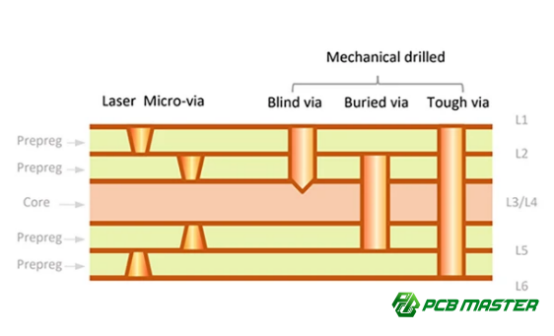
1. CNC drilling for through-holes and vias
After lamination, CNC drilling machines create precise holes in the PCB.
These holes include:
- Through-holes for component leads
- Vias connecting internal copper layers
Modern CNC drilling in PCB manufacturing allows extremely accurate hole positioning.
Example: In compact electronic products, microvias help engineers route signals through dense multilayer PCB layouts.
2. Copper plating for electrical interconnection between layers
After drilling, the hole walls are coated with copper through an electroplating process.
This creates conductive pathways connecting all required layers electrically.
Purpose of PCB copper plating:
- Enable signal transfer between layers
- Ensure stable current flow
- Improve mechanical strength of vias
Example: Without proper via plating, signals could stop between layers, causing complete circuit failure.
PCBMASTER uses strict plating thickness control to ensure reliable interlayer conductivity.
PCBMASTER quality control during manufacturing
PCBMASTER applies multiple inspection and testing processes during 6-layer PCB manufacturing to ensure high reliability and stable electrical performance.
1. Automated optical inspection (AOI) for defect detection
AOI systems scan PCB layers using high-resolution cameras to detect manufacturing defects automatically.
Common defects detected:
- Open circuits
- Short circuits
- Missing copper patterns
- Trace width errors
Benefit: AOI improves production accuracy and reduces human inspection errors.
2. Electrical testing to ensure continuity and isolation
Finished boards undergo electrical testing to verify all designed connections.
Testing checks:
- Continuity between connected circuits
- Isolation between unrelated circuits
This step ensures the PCB functions correctly before shipment.
Example :A failed isolation test may indicate an internal short circuit between power and ground layers.
3. Strict impedance and thickness verification
In controlled impedance 6-layer PCB manufacturing, PCBMASTER verifies layer thickness, dielectric spacing, and impedance values.
This is especially important for:
- High-speed digital circuits
- RF communication boards
- Networking equipment
Result:
- Stable signal transmission
- Reduced signal reflection and EMI problems
PCBMASTER uses impedance testing and microsection analysis to ensure every multilayer PCB meets customer specifications.

What are the key design rules for 6-layer PCB stack-up optimization?
The key design rules for 6-layer PCB stack-up optimization focus on signal integrity, impedance control, thermal management, and reliable layer structure. A well-optimized stack-up improves electrical performance, reduces EMI, and increases manufacturing stability.
In 6-layer PCB stack-up design optimization, engineers must carefully control trace routing, via structure, layer spacing, and heat dissipation. Small design improvements can greatly improve long-term PCB reliability and high-speed signal performance.
Impedance control in high-speed signal routing
Impedance control in a 6-layer PCB stack-up helps high-speed signals travel smoothly without reflection, distortion, or data loss.
1. Controlled dielectric spacing for impedance matching
In controlled impedance PCB design, the distance between signal layers and reference planes directly affects impedance values.
Dielectric materials between layers act like electrical spacing controls. If the spacing changes too much, signal impedance also changes.
Why this matters:
- Stable impedance improves signal quality
- Reduces signal reflections in high-speed circuits
- Supports reliable data transmission
Example: USB, HDMI, DDR memory, and Ethernet signals all require accurate impedance control.
PCBMASTER carefully controls dielectric thickness during multilayer PCB fabrication to maintain stable impedance values.
2. Importance of consistent trace width and spacing
In a high-speed 6-layer PCB layout, signal traces must maintain consistent width and spacing across the board.
Changing trace width suddenly can change impedance and create signal reflections.
Best practices:
- Keep trace widths uniform
- Maintain equal spacing in differential pairs
- Avoid unnecessary sharp corners
Simple comparison: A smooth, straight road allows cars to move easily. Sudden narrow sections create traffic problems. Signal traces behave similarly.
Consistent routing improves signal integrity and reduces EMI problems in high-speed PCB designs.
Via design considerations in multilayer boards
Via design in a 6-layer PCB affects routing density, signal quality, and high-frequency electrical performance.
1. Use of blind and buried vias for dense routing
Modern multilayer PCB via design often uses blind vias and buried vias to save routing space.
- Blind vias connect an outer layer to inner layers
- Buried vias connect only internal layers
These vias allow more routing channels in compact PCB layouts.
Benefits:
- Higher routing density
- Smaller PCB size
- Better support for complex electronic systems
Example:
Smart communication devices and embedded systems often use blind vias to fit more circuits into limited board space.
2. Minimizing via stub effects in high-frequency designs
A via stub is an unused portion of a via that can create signal reflections in high-frequency PCB designs.
Long via stubs act like small antennas, causing signal loss and EMI issues.
Optimization methods:
- Use back drilling
- Reduce unused via length
- Keep high-speed vias as short as possible
Example:
In high-speed networking equipment, reducing via stubs helps maintain clean data transmission at high frequencies.
PCBMASTER recommends careful via optimization for high-speed multilayer PCB applications.
Thermal management in 6-layer PCB structures
Thermal management in a 6-layer PCB stack-up helps remove heat from components and improves long-term reliability.
1. Heat spreading through ground planes
Ground planes in a 6-layer PCB thermal design do more than provide electrical grounding. They also spread heat across the board.
Large copper planes distribute heat away from hot components, reducing local temperature buildup.
Benefits:
- Lower operating temperatures
- Improved component lifespan
- Better system stability
Example:
Power regulators and processors generate heat continuously. Ground planes help prevent overheating during operation.
2. Use of thermal vias for component cooling
Thermal vias are small plated holes placed under heat-generating components.
These vias transfer heat from the top layer to internal copper planes or bottom layers.
Advantages of thermal vias:
- Faster heat dissipation
- Better cooling efficiency
- Reduced risk of thermal damage
Example:
LED drivers and power MOSFETs often use thermal vias to maintain safe operating temperatures.
PCBMASTER commonly applies thermal via arrays in power-heavy multilayer PCB designs.
PCBMASTER design optimization tips
PCBMASTER recommends several practical design rules to improve signal integrity, manufacturability, and reliability in 6-layer PCB stack-up design.
1. Avoid crossing split planes under sensitive signals
Sensitive high-speed traces should never cross gaps or split areas in ground or power planes.
When signals cross split planes, the return current path becomes unstable, increasing EMI and signal noise.
Best practice:
- Keep continuous reference planes under critical signals
- Avoid routing across plane boundaries
Example:
Crossing a split ground plane can cause communication errors in Ethernet or USB circuits.
2. Use symmetrical stack-ups to reduce board warping
A symmetrical 6-layer PCB stack-up balances copper distribution and dielectric thickness on both sides of the board.
This helps reduce:
- PCB warping
- Mechanical stress
- Assembly alignment problems
Example:
An unbalanced multilayer PCB may bend during soldering, causing poor component connections.
PCBMASTER recommends symmetrical layer structures for stable manufacturing results.
3. Optimize return path continuity for signal integrity
Every high-speed signal needs a clean return current path through nearby ground planes.
Poor return path continuity increases:
- Signal noise
- EMI emissions
- Timing instability
Best practice:
- Keep ground planes continuous
- Place vias near signal transitions
- Minimize interruptions in return current flow
Simple explanation:
Electric signals work best when they can “go out and come back” smoothly without obstacles.
PCBMASTER uses signal integrity analysis and stack-up optimization to improve return path performance in high-speed PCB applications.
What are common challenges in 6-layer PCB stack-up manufacturing?
Common challenges in 6-layer PCB stack-up manufacturing include layer alignment problems, lamination stress, signal integrity issues, and impedance inconsistencies. These problems can affect electrical performance, production yield, and long-term reliability.
In multilayer PCB manufacturing, tighter tolerances and more complex layer structures make process control more difficult than in 2-layer or 4-layer PCBs. High-speed applications require especially careful stack-up planning and manufacturing precision.
Layer misalignment and lamination stress issues
Layer misalignment and lamination stress are common manufacturing challenges that can reduce PCB accuracy, reliability, and production yield.
1. Causes of registration errors during lamination
In 6-layer PCB lamination, all internal layers must align precisely before pressing and bonding.
Registration errors can happen because of:
- Material expansion during heating
- Improper layer positioning
- Uneven pressure during lamination
- Dimensional changes in prepreg materials
Even small alignment shifts can cause vias and pads to miss their intended locations.
Example: If drilled holes do not align with internal copper pads, electrical connections may fail completely.
PCBMASTER uses precision alignment systems to reduce multilayer PCB registration errors during production.
2. Impact on electrical performance and yield
Poor layer alignment can directly affect electrical performance in multilayer PCB manufacturing.
Common problems include:
- Open circuits
- Short circuits
- Weak interlayer connections
- Signal instability
Misalignment also lowers manufacturing yield because defective boards may fail testing or require rework.
Simple comparison: It is similar to stacking transparent sheets with printed lines. If the sheets shift, the lines no longer connect correctly.
In high-speed PCB applications, even small alignment problems can reduce signal integrity and reliability.
Signal integrity degradation in high-speed designs
Signal integrity problems in 6-layer PCB stack-ups can cause data errors, signal loss, and unstable system performance.
1. Crosstalk between adjacent layers
Crosstalk in multilayer PCB design happens when signals from one trace interfere with nearby traces.
In dense high-speed layouts, electromagnetic fields can couple between adjacent signal layers or traces.
Effects of PCB crosstalk:
- Data corruption
- Increased signal noise
- Reduced communication stability
Example: In networking equipment, crosstalk may cause unstable data transmission between communication channels.
Proper layer spacing and ground plane placement help reduce crosstalk in high-speed PCB stack-up designs.
2. Impedance discontinuities due to poor stack-up planning
An impedance discontinuity happens when signal impedance changes suddenly along the routing path.
This problem is often caused by:
- Incorrect layer spacing
- Inconsistent trace width
- Poor via transitions
- Split reference planes
Impedance discontinuities create signal reflections and timing problems.
Example: In HDMI or Ethernet designs, poor impedance control can lead to signal distortion or communication errors.
PCBMASTER recommends controlled impedance planning early in the PCB stack-up design stage.
PCBMASTER manufacturing solutions for reliability
PCBMASTER uses advanced manufacturing control methods to improve multilayer PCB reliability, signal stability, and production consistency.
1. Precision alignment systems during lamination
PCBMASTER uses high-accuracy optical alignment systems during multilayer PCB lamination.
These systems help:
- Maintain accurate layer registration
- Reduce drilling offset issues
- Improve interlayer connection reliability
Precise alignment is especially important in dense 6-layer PCB stack-up manufacturing.
2. Advanced impedance simulation before production
Before production begins, PCBMASTER performs PCB impedance simulation and stack-up analysis.
Simulation helps engineers verify:
- Trace impedance values
- Layer spacing accuracy
- Signal integrity performance
This reduces the risk of impedance mismatch problems during manufacturing.
Example: A communication PCB designed for 100Ω differential signals can be verified before fabrication starts.
3. Strict process control for multilayer consistency
PCBMASTER applies strict process monitoring throughout every manufacturing stage.
Key controls include:
- Lamination temperature monitoring
- Copper thickness verification
- Dielectric thickness control
- AOI and electrical testing
These controls improve:
- PCB consistency
- Manufacturing yield
- Long-term product reliability
Simple explanation: Careful process control keeps every PCB “built the same way,” reducing unexpected performance problems in the final product.
How does PCBMASTER ensure high-quality 6-layer PCB stack-up production?
PCBMASTER ensures high-quality 6-layer PCB stack-up production through engineering verification, strict manufacturing control, automated inspection systems, and customized technical support. The goal is to deliver multilayer PCBs with stable electrical performance, accurate impedance control, and long-term reliability.
In 6-layer PCB manufacturing, quality must be controlled before, during, and after production. PCBMASTER combines design analysis, process monitoring, and final testing to reduce defects and improve production consistency.
Engineering validation before manufacturing
PCBMASTER performs engineering validation before production to identify design risks early and improve manufacturability.
1. Stack-up simulation and DFM (Design for Manufacturability) checks
Before manufacturing begins, PCBMASTER engineers review the PCB design using stack-up simulation and DFM analysis.
DFM checks help verify:
- Layer structure feasibility
- Minimum trace width and spacing
- Via design reliability
- Manufacturing tolerance compatibility
Stack-up simulation is used to confirm:
- Controlled impedance values
- Layer spacing accuracy
- Signal integrity performance
Example:
If a trace is too narrow for stable production, PCBMASTER provides recommendations before fabrication starts.
This early review helps reduce production delays and PCB failure risks.
2. Early design feedback to avoid production risks
PCBMASTER provides early engineering feedback to customers during the PCB development stage.
This helps identify:
- Potential impedance mismatches
- Thermal management problems
- Layer imbalance issues
- Manufacturing limitations
Benefits of early PCB design feedback:
- Lower production cost
- Faster project turnaround
- Improved manufacturing yield
Example:
If a customer design may cause board warping during lamination, PCBMASTER can recommend a more symmetrical stack-up structure before production begins.
Production quality assurance systems
PCBMASTER uses multiple inspection and testing systems during manufacturing to ensure consistent multilayer PCB quality.
1. Automated inspection at every manufacturing stage
PCBMASTER applies automated PCB inspection systems throughout production.
Inspection stages include:
- Inner layer imaging
- Etching verification
- Drilling inspection
- Final surface inspection
Automated optical inspection (AOI) systems detect:
- Open circuits
- Short circuits
- Missing copper
- Trace defects
Benefit:
Automated inspection improves accuracy and reduces human error in multilayer PCB manufacturing.
2. Electrical testing for open/short detection
Every finished 6-layer PCB undergoes electrical testing before shipment.
The testing process verifies:
- Proper electrical continuity
- Isolation between unrelated circuits
- Stable interlayer connections
Why this matters:
Even invisible internal defects can cause electronic failure after assembly.
Example:
A hidden short circuit between power and ground layers can prevent the device from powering on correctly.
PCBMASTER uses high-precision electrical testing equipment to improve delivery reliability.
3. Microsection analysis for layer bonding quality
PCBMASTER performs microsection analysis to inspect the internal structure of multilayer PCBs.
Small PCB samples are cut and examined under a microscope to verify:
- Copper plating thickness
- Via wall quality
- Layer bonding condition
- Lamination consistency
Purpose of PCB microsection testing:
- Ensure strong interlayer connections
- Detect hidden structural defects
- Verify compliance with PCB specifications
This process is especially important for high-reliability industrial and automotive PCB applications.
PCBMASTER value-added services
PCBMASTER provides engineering support and flexible production services to help customers optimize 6-layer PCB stack-up performance and manufacturing efficiency.
1. Engineering consultation for stack-up optimization
PCBMASTER engineers help customers optimize:
- Layer arrangements
- Impedance control structures
- Thermal management designs
- EMI shielding strategies
This support improves:
- Signal integrity
- Manufacturability
- Product reliability
Example:
For high-speed communication PCBs, PCBMASTER may recommend additional ground plane shielding to reduce EMI.
2. Fast prototyping and mass production scalability
PCBMASTER supports both rapid PCB prototyping and high-volume production.
Advantages include:
- Faster product development cycles
- Easy transition from prototype to mass production
- Consistent multilayer PCB quality across production batches
Example:
A startup developing an IoT device can begin with small prototype quantities and later scale to full production without redesigning the PCB process.
3. Custom impedance-controlled PCB solutions
PCBMASTER provides custom impedance-controlled 6-layer PCB manufacturing for high-speed and high-frequency applications.
Custom solutions include:
- Differential impedance control
- High-speed stack-up optimization
- Low-loss material recommendations
- Signal integrity verification
Applications include:
- Networking equipment
- Automotive electronics
- Industrial control systems
- Embedded computing devices
PCBMASTER helps customers achieve stable signal performance while balancing cost and manufacturability.
When should you choose a 6-layer PCB instead of other multilayer designs?
A 6-layer PCB should be chosen when a project needs better signal integrity, EMI control, and routing space than a 4-layer board can provide, but does not require the higher cost and complexity of an 8-layer PCB.
In modern electronics, a 6-layer PCB stack-up is often the best balance between electrical performance, manufacturing cost, and design flexibility. It is widely used in industrial electronics, communication devices, embedded systems, and automotive applications.
Comparison between 4-layer, 6-layer, and 8-layer PCBs
The main difference between 4-layer, 6-layer, and 8-layer PCBs is their routing capacity, signal performance, EMI control, and support for high-speed circuits.
1. 4-layer PCB: basic routing and low-speed applications
A 4-layer PCB is commonly used for simple or medium-complexity electronics.
Typical structure:
- Top signal layer
- Ground plane
- Power plane
- Bottom signal layer
Advantages:
- Lower manufacturing cost
- Simpler stack-up design
- Suitable for low-speed circuits
Limitations:
- Limited routing space
- Reduced EMI shielding
- Less effective for dense layouts
Example:
Basic consumer electronics and small control boards often use 4-layer PCB designs.
2. 6-layer PCB: balanced performance and cost efficiency
A 6-layer PCB stack-up adds extra signal and ground layers, improving routing flexibility and electrical stability.
Advantages of 6-layer PCB design:
- Better signal integrity
- Improved EMI control
- Higher routing density
- More stable power distribution
This makes 6-layer boards ideal for:
- Industrial controllers
- Networking devices
- Embedded systems
- Automotive electronics
Example:
A communication router may use a 6-layer PCB to support stable high-speed data transmission without excessive manufacturing cost.
3. 8-layer PCB: high-speed and complex systems
An 8-layer PCB is designed for advanced high-speed and high-density applications.
Additional layers provide:
- More routing channels
- Better isolation between signals
- Stronger EMI shielding
- Advanced impedance control
However, 8-layer boards also increase:
- Manufacturing complexity
- Production cost
- Stack-up design requirements
Example:
Servers, AI computing systems, and high-frequency RF equipment often require 8-layer PCB designs.
Comparison Table
| PCB Type | Main Advantages | Main Limitations | Best Application Scenarios | Typical Example |
| 4-Layer PCB |
|
|
|
Smart home devices, simple controllers, LED control boards |
| 6-Layer PCB |
|
|
|
Communication routers, industrial gateways, automotive control modules |
| 8-Layer PCB |
|
|
|
AI servers, high-frequency RF systems, data center networking equipment |
Application-based decision criteria
Choosing between 4-layer, 6-layer, and 8-layer PCBs depends on signal speed, EMI requirements, and available PCB space.
1. Signal speed requirements
High-speed signals require better impedance control and cleaner return paths.
A 6-layer PCB for signal integrity is often preferred when:
- Data rates increase
- Differential pairs are used
- Signal reflections must be minimized
General guideline:
- Low-speed products → 4-layer PCB
- Medium/high-speed products → 6-layer PCB
- Very high-speed systems → 8-layer PCB
Example:
Gigabit Ethernet and DDR memory designs usually perform better on 6-layer or higher stack-ups.
2. EMI/EMC compliance needs
Products operating in noisy electrical environments often need stronger EMI shielding.
A 6-layer PCB stack-up for EMI reduction provides additional ground planes that help control electromagnetic interference.
This is important for:
- Automotive electronics
- Industrial automation systems
- Communication equipment
Example:
Industrial motor controllers may fail EMC testing if the PCB stack-up does not provide enough shielding.
3. Space constraints in product design
Compact electronic products require higher routing density.
Additional PCB layers allow engineers to route more signals internally instead of crowding the outer layers.
Benefits of multilayer PCB routing:
- Smaller board size
- Cleaner layout organization
- Better support for compact devices
Example:
Embedded IoT systems often use 6-layer PCB designs to fit more functionality into small enclosures.
PCBMASTER recommendation for engineers
PCBMASTER recommends selecting PCB layer counts based on real electrical and mechanical requirements rather than choosing more layers unnecessarily.
1. Choose 6-layer when performance and cost must be balanced
For many modern electronic products, a 6-layer PCB stack-up provides the best balance between:
- Signal quality
- EMI control
- Manufacturing cost
- Routing flexibility
PCBMASTER often recommends 6-layer designs for:
- Industrial electronics
- Communication hardware
- Embedded control systems
- Automotive modules
Example:
A smart industrial gateway can achieve reliable high-speed communication using a well-optimized 6-layer PCB without the added cost of an 8-layer structure.
2. Upgrade to 8-layer only for high-frequency or dense systems
PCBMASTER recommends moving to an 8-layer PCB design only when the application truly requires:
- Extremely dense routing
- Advanced high-frequency performance
- Stronger isolation between signals
- Multiple power domains
Using unnecessary layers can increase:
- PCB manufacturing cost
- Lamination complexity
- Production lead time
Simple recommendation:
Use the simplest stack-up that still meets the electrical and mechanical requirements of the product.
Conclusion
A well-designed 6-layer PCB stack-up offers the ideal balance between performance, reliability, and cost for many modern electronic applications. Compared with simpler multilayer designs, it provides better signal integrity, stronger EMI control, higher routing density, and more stable power distribution, making it an excellent choice for industrial systems, communication devices, automotive electronics, and embedded applications.
However, achieving reliable 6-layer PCB performance depends on more than just adding extra layers. Material selection, stack-up structure, impedance control, thermal management, and manufacturing precision all play critical roles in final product quality.
At PCBMASTER, we combine engineering expertise, advanced manufacturing technology, and strict quality control to help customers develop high-performance multilayer PCB solutions with confidence. From stack-up optimization and impedance-controlled design to prototyping and mass production, PCBMASTER supports every stage of the PCB manufacturing process.
If you are looking for a reliable partner for 6-layer PCB stack-up manufacturing, PCBMASTER is ready to help you achieve stable performance, efficient production, and long-term product reliability.
FAQs
What is the typical layer order in a 6-layer PCB stack-up?
A typical 6-layer PCB stack-up uses a balanced structure designed for signal integrity and EMI control.
One common layer arrangement is:
- Top Signal Layer
- Ground Plane
- Inner Signal Layer
- Power Plane
- Ground Plane
- Bottom Signal Layer
This structure keeps signal layers close to ground planes, which helps reduce noise and improve signal stability. The exact stack-up may vary depending on the application, impedance requirements, and routing density.
Why are ground planes important in multilayer PCB design?
Ground planes are important because they provide a stable return path for electrical signals and help reduce electromagnetic interference (EMI).
In a multilayer PCB, ground planes improve:
- Signal integrity
- Noise reduction
- Power stability
- EMI shielding
A solid ground plane also lowers return path impedance, allowing high-speed signals to travel more cleanly and reliably.
For high-speed PCB designs, continuous ground planes are essential for stable electrical performance.
Can 6-layer PCBs support high-speed signal transmission?
Yes. A 6-layer PCB is widely used for high-speed signal transmission because it offers better impedance control, cleaner return paths, and improved EMI shielding compared to 2-layer or 4-layer boards.
The additional layers allow engineers to:
- Separate signal and power routing
- Add dedicated ground planes
- Reduce crosstalk between traces
- Maintain controlled impedance
This makes 6-layer PCB stack-ups suitable for Ethernet, DDR memory, USB, HDMI, and other high-speed digital applications.
What industries commonly use 6-layer PCB designs?
6-layer PCB designs are commonly used in industries that require stable signal performance, compact layouts, and reliable power distribution.
Common applications include:
- Industrial automation systems
- Automotive electronics
- Communication and networking equipment
- Embedded systems
- Medical devices
- IoT products
For example, routers, industrial controllers, and automotive ECUs often use 6-layer PCB stack-ups to improve signal integrity and reduce EMI problems.
How does PCBMASTER ensure impedance control accuracy?
PCBMASTER ensures impedance control accuracy through stack-up simulation, controlled material selection, and strict manufacturing process control.
Key methods include:
- Impedance calculation during PCB design
- Controlled dielectric thickness verification
- Precision trace width control
- Advanced impedance simulation before production
- Test coupon measurement after fabrication
PCBMASTER also performs impedance testing and microsection analysis to verify that the finished multilayer PCB meets customer impedance specifications for high-speed applications.
About the Author

Carol Luo
PCB Design EngineerI'm Carol, a PCB Engineer at PCBMASTER with experience in PCB design and manufacturing engineering since 2018. I focus on translating engineering requirements into reliable PCB solutions, with expertise in stack-up design, material selection, and design-for-manufacturing (DFM). I share practical engineering insights from real-world PCB design and production experience.
Visit Carol Luo's Profile