


Top PCB Design for Manufacturing Tips Every Engineer Should Know
PCB Design for Manufacturing (DFM) is the practice of designing printed circuit boards in a way that makes them easy, reliable, and cost-effective to produce. By considering manufacturing constraints during the design phase, engineers can prevent common issues like soldering defects, misaligned components, and production delays. Implementing DFM principles improves overall yield, reduces rework, and ensures that the final product performs reliably in the field.
DFM is not just a technical guideline—it is a strategic approach to saving time and money while improving quality. For example, proper component placement and spacing can minimize assembly errors, while careful via and pad design ensures smooth soldering. These practical adjustments help manufacturers like PCBMASTER produce boards efficiently without compromising performance.
As an experienced PCB and PCBA supplier, PCBMASTER has worked closely with engineers to provide guidance on DFM best practices. This article shares actionable tips and proven strategies that every engineer should know to design boards that are manufacturing-friendly. Readers will learn how to optimize layouts, avoid costly mistakes, and collaborate effectively with PCB manufacturers to create high-quality, production-ready boards.
What Is PCB Design for Manufacturing and Why Is It Critical?
PCB Design for Manufacturing (DFM) is the practice of designing printed circuit boards in a way that makes them easy, reliable, and cost-effective to manufacture. It goes beyond just making the board work electrically—it ensures the design aligns with real-world production capabilities.
Defining PCB DFM
PCB DFM is a set of design guidelines that help engineers create boards that are manufacturable without errors or delays.
PCB Design for Manufacturing, or DFM, focuses on designing PCBs that factories can produce efficiently. Unlike basic PCB design, which mainly ensures that circuits work electrically, DFM looks at how the design interacts with real manufacturing processes like drilling, soldering, and assembly. For example, a DFM-focused design will use proper trace widths, spacing, and pad sizes to prevent shorts or misaligned components during production.
Comparison: Imagine building a toy car. A basic design ensures it moves, but a DFM approach makes sure it can be mass-produced without parts breaking or assembly slowing down. Similarly, DFM ensures the PCB works and can be reliably manufactured at scale.
Benefits of Applying DFM Practices
Applying DFM in PCB design improves production yield, reduces rework, and lowers costs.
Higher Manufacturing Yield
Boards designed with DFM guidelines are less likely to fail during production. Proper pad spacing, trace widths, and drill tolerances reduce errors, increasing the number of usable boards per batch.
Reduced Rework and Production Delays
DFM helps avoid common mistakes that cause soldering defects or assembly errors. Fewer mistakes mean fewer boards need correction, saving time and preventing delays.
Cost Optimization
By designing with manufacturing limits in mind, DFM avoids expensive special processes or excessive scrap. For example, using standard hole sizes instead of microvias where unnecessary can reduce drilling costs.
Real-Life Example: A PCB with tight trace spacing failed during mass production. Redesigning with DFM guidelines allowed the factory to produce 95% of boards successfully on the first run, saving time and thousands in costs.
PCBMASTER’s Perspective on DFM
PCBMASTER ensures all customer designs follow DFM principles, improving manufacturability and production success.
Ensuring DFM Compatibility: PCBMASTER reviews each PCB design using automated DFM checks and design rule verifications. These checks highlight issues like trace spacing, pad sizes, and via placement. Engineers then adjust the design to match manufacturability standards.
Real-World Example: A client submitted a high-speed multilayer PCB with challenging via structures. PCBMASTER recommended minor adjustments to layer stack-up and via diameters. The resulting board passed all assembly tests on the first try, reducing lead time and preventing costly delays.

How Can Engineers Optimize PCB Layout for Manufacturing?
Engineers optimize PCB layouts by placing components thoughtfully, routing traces efficiently, and selecting the right materials and layer structures. These steps make manufacturing easier, reduce errors, and save costs.
Proper Component Placement Strategies
Proper component placement ensures smooth automated assembly, easier testing, and fewer production mistakes.
Placing similar components together, such as resistors, capacitors, or connectors, helps assembly machines work faster and reduces the chance of misplacement. For example, grouping all SMD resistors in one area allows pick-and-place machines to handle them efficiently. Orienting components consistently, with all facing the same direction when possible, minimizes handling errors and soldering defects. Boards with random orientations often require slower machine speeds and higher inspection effort.
Access for testing and rework is another key factor. Leaving space around critical components and including test points makes quality checks easier. At PCBMASTER, engineers design boards with enough spacing around ICs and connectors so that probes and manual soldering tools can reach components without risk of damage. This approach reduces rework and improves first-pass yield.
Efficient Routing Practices
Routing traces correctly ensures electrical performance while reducing manufacturing problems.
Trace width and spacing should meet the manufacturer’s minimum requirements. Too narrow or closely spaced traces can cause shorts or open circuits. For example, a 1 oz copper board usually requires at least 6 mil spacing and 6 mil width for standard signal lines. Avoiding sharp angles and long parallel traces prevents manufacturing defects and signal interference. A 45° corner is preferred over a 90° corner because it reduces the risk of etching problems, and parallel traces in high-speed circuits can cause crosstalk.
High-speed signals require controlled impedance, which means keeping trace width and spacing consistent. This is critical for preventing signal reflections or losses. PCBMASTER provides guidance for microstrip and stripline routing in high-speed designs such as DDR memory or USB circuits, ensuring the board functions correctly and is easy to manufacture.
Layer Stack-Up and Material Considerations
Choosing the right materials and layer structure balances performance, manufacturability, and cost.
Selecting standard FR4 material works well for most low- to mid-frequency designs, keeping production simple and cost-effective. For high-frequency designs, specialized materials like Rogers may be necessary to maintain signal integrity. Optimizing layer count also helps reduce cost. Using the minimum number of layers needed for electrical performance reduces lamination complexity and production time. For instance, careful routing can allow a 6-layer board to replace an 8-layer design.
PCBMASTER recommends stack-ups that separate signal, power, and ground layers strategically. Common practices include placing signal layers next to ground planes to control impedance and reduce electromagnetic interference. High-speed and analog signals are often routed on different layers to prevent interference, improving both performance and manufacturability.
What Are Key Drilling and Via Design Tips for DFM?
Key drilling and via design tips focus on choosing the right hole sizes, via types, and placement strategies to ensure boards are manufacturable, reliable, and cost-effective. Proper planning reduces defects and improves assembly efficiency.
Choosing the Right Hole Sizes and Tolerances
Selecting proper hole sizes and managing tolerances ensures that drilled holes are compatible with automated production and multilayer board assembly.
Using standard drill sizes simplifies manufacturing and reduces costs. Most factories, including PCBMASTER, have preferred hole diameters for through-holes, typically ranging from 0.2 mm to 1.0 mm for standard components. Avoid using extremely small or non-standard holes unless necessary, as they increase drilling difficulty and may cause misalignment.
Tolerance is critical in multilayer boards. Each layer must align accurately during lamination, or vias can miss their target pads. Minimizing tolerance issues means designing holes slightly larger than the minimum required for plating and assembly. For example, if a 0.3 mm hole is specified, adding 0.05 mm can improve yield without affecting functionality. This approach reduces rejected boards and improves first-pass manufacturing success.
Via Types and Their Manufacturing Implications
Choosing the right type of via affects manufacturing complexity, cost, and board reliability.
Through-hole vias pass all the way through the board and are easy to produce. Blind vias connect outer layers to inner layers without going through the entire board, while buried vias connect only inner layers. Blind and buried vias are more expensive and require precise fabrication. Using them only when necessary balances performance and cost.
Microvias are small vias typically used in high-density boards or HDI designs. PCBMASTER recommends microvias for signal layers with limited space, but advises avoiding excessive use to reduce risk of open or incomplete plating. Choosing the correct via type early in the design phase ensures manufacturability and prevents rework.
Via Placement and Thermal Considerations
Proper via placement prevents thermal stress, improves reliability, and ensures easier manufacturing.
Vias placed near heat-sensitive components or in high-current paths can cause thermal stress, potentially leading to solder joint cracks or delamination. It is best to keep vias slightly away from IC pads or use thermal relief patterns to distribute heat.
Good via placement balances signal routing, mechanical strength, and thermal management. For example, placing multiple small vias under a power pad spreads heat evenly, while a single via can create a hot spot. Bad layouts include clustered vias that interfere with soldering or obstruct inspection. PCBMASTER often reviews via placement in DFM checks, adjusting positions to avoid assembly problems while maintaining electrical performance.
How Should Engineers Design PCB Pads and Footprints for Reliable Assembly?
Engineers design PCB pads and footprints to ensure strong solder joints, accurate component placement, and smooth assembly. Proper pad design reduces errors, improves yield, and supports automated manufacturing.
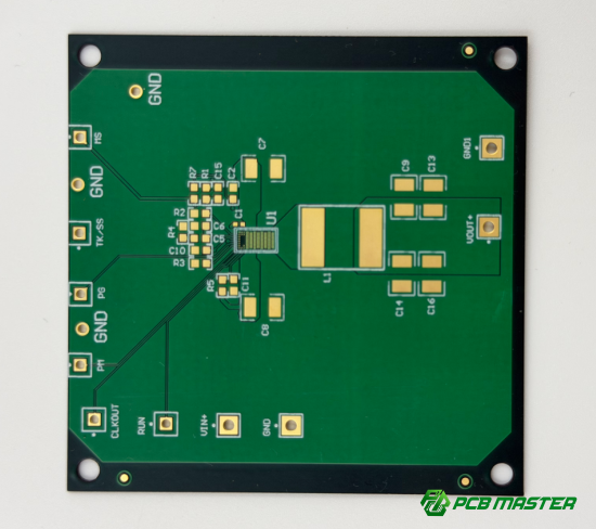
Optimal Pad Sizes and Shapes
Choosing the right pad sizes and shapes for each component type ensures reliable solder joints and easy assembly.
Pad design varies between SMD (surface-mount devices) and through-hole components. SMD pads are usually smaller and flat, requiring precise sizing for automated pick-and-place machines. Through-hole pads are larger and allow the lead to pass through the board. Proper pad size ensures a good solder fillet—the small triangle of solder connecting the pad to the component—improving mechanical and electrical reliability. For example, too small a pad may prevent full solder wetting, while an overly large pad may cause solder bridging. PCBMASTER guides engineers on pad dimensions based on component datasheets and assembly capabilities.
Silkscreen and Solder Mask Considerations
Correct silkscreen and solder mask design prevents assembly errors and improves readability during production.
Silkscreen markings must avoid overlapping pads to prevent accidental solder interference. Clear labels indicate component orientation and placement, which is crucial for automated assembly lines. The solder mask protects pads from excess solder and prevents shorts. For example, misaligned silkscreen over a resistor pad can confuse assembly robots or technicians. PCBMASTER emphasizes maintaining at least 0.1 mm clearance between silkscreen and pads and verifying solder mask openings for each footprint. This practice reduces assembly mistakes and inspection issues.
Footprint Verification Tips
Verifying footprints ensures components fit correctly and reduces assembly errors before production.
Using verified design libraries helps engineers apply standardized footprints that meet manufacturer guidelines. DFM checks automatically detect problems like incorrect pad size, misaligned pins, or insufficient solder mask clearance. PCBMASTER recommends reviewing each footprint with automated tools and cross-checking against component datasheets. For example, a capacitor footprint with incorrect pad spacing could cause placement failure or poor soldering, delaying production. Following these verification steps ensures the PCB is ready for reliable assembly and reduces costly rework.
How Can Engineers Minimize Manufacturing Risks and Improve Yield?
Engineers can reduce manufacturing risks and improve yield by managing thermal stress, optimizing panel layouts, including test points, and avoiding common design mistakes that lead to defects. These strategies help produce reliable PCBs while lowering costs and rework.
Thermal Management During Assembly
Proper thermal management prevents component damage and ensures successful soldering during assembly.
Excessive heat can damage sensitive components like LEDs, ICs, and certain capacitors. Engineers should carefully place heat-sensitive components away from high-temperature zones such as power regulators or areas with large copper pours. Using thermal relief pads can also help distribute heat evenly during soldering. For example, PCBMASTER often places microcontrollers and delicate ICs away from large copper planes to prevent overheating, ensuring solder joints remain strong and reliable. Proper thermal planning reduces assembly failures and increases first-pass yield.
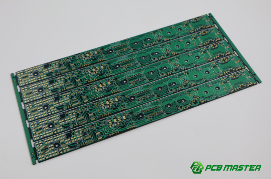
Panelization and Test Point Planning
Optimizing PCB panelization and including test points streamlines automated assembly and quality inspection.
Panelization combines multiple PCBs into a single sheet for efficient automated assembly. Engineers should design panel sizes compatible with pick-and-place machines, keeping spacing sufficient to prevent board warping. Including test points at critical signals allows in-line automated electrical checks, catching faults before final assembly. For example, adding a few test points on power rails and communication lines enables quick functional testing. PCBMASTER recommends standardizing panel dimensions and test point placement, reducing production errors and improving overall yield.
Common Pitfalls and How to Avoid Them
Avoiding typical design mistakes prevents yield loss and costly rework in PCB manufacturing.
Common errors include traces that are too close, improper pad sizes, poorly placed vias, or inconsistent solder mask coverage. These issues can cause shorts, open circuits, or soldering defects. Preventive measures include following manufacturer design rules, using DFM verification tools, and reviewing critical areas such as high-current paths and dense component zones. For example, a board with insufficient trace spacing between power and signal lines caused multiple shorts; redesigning the spacing according to DFM rules eliminated failures. PCBMASTER helps engineers identify and correct these pitfalls early, improving reliability and reducing scrap rates.
What Tools and Checks Can Help Ensure DFM Compliance?
Engineers can ensure DFM compliance by using design rule checks, automated DFM software, and collaborating with PCB manufacturers. These tools catch design issues early and improve production success.
Design Rule Checks (DRC)
DRC helps verify that a PCB design meets manufacturing constraints for spacing, drills, pads, and other critical parameters.
A Design Rule Check (DRC) automatically scans a PCB layout to identify violations of spacing, trace width, pad size, and drill hole rules. These checks prevent issues like shorts, misaligned vias, or pads that are too small for soldering. PCBMASTER recommends DRC settings tailored to standard manufacturing tolerances—for example, minimum 6 mil trace spacing, 6 mil pad clearance for SMD, and drill tolerances of ±0.05 mm. By catching errors early in the design phase, DRC reduces rework and prevents delays in assembly. This step is essential for both single-layer and complex multilayer PCBs.
Automated DFM Analysis Software
AI-assisted DFM software identifies potential manufacturing issues faster and more accurately than manual review.
Automated DFM analysis tools evaluate PCB layouts against a wide range of manufacturing rules, including pad-to-pad spacing, via placement, solder mask coverage, and thermal relief. These tools can flag potential defects that may be overlooked by human designers, improving first-pass yield. Integration into popular PCB design software, such as Altium Designer, KiCad, or Cadence Allegro, allows engineers to run checks without leaving their design environment. For example, PCBMASTER uses AI-assisted tools to highlight areas where soldering defects could occur on high-density boards, enabling designers to make adjustments before production.
Collaboration With PCB Manufacturers
Brief Answer: Early communication with PCB manufacturers ensures designs meet real-world production capabilities, reducing errors and delays.
Working closely with manufacturers allows engineers to adjust designs for factors such as drill capabilities, layer stack-ups, and material limits. PCBMASTER provides DFM review services where engineers evaluate submitted designs and suggest changes to improve manufacturability. This collaborative approach can prevent common pitfalls, like impractical via structures or trace widths that exceed machine tolerances. For example, a client submitted a high-speed board with challenging microvias; early consultation with PCBMASTER allowed adjustments that avoided costly production errors and shortened lead times.
Conclusion
Implementing PCB Design for Manufacturing (DFM) principles helps engineers create boards that are easier to produce, more reliable, and cost-effective. Key tips include thoughtful component placement, efficient trace routing, careful via selection, optimal pad and footprint design, and proper test point planning. Collaborating closely with manufacturers and using tools like DRC and automated DFM analysis further ensures designs meet production capabilities.
DFM practices directly improve yield by reducing errors, soldering defects, and assembly delays. Boards designed with DFM in mind require less rework, consume fewer materials, and save both time and money, making them ideal for both prototypes and mass production.
PCBMASTER works with engineers to implement these tips in real-world projects, offering guidance on manufacturable layouts, layer stack-ups, and DFM reviews. By combining experience, advanced tools, and hands-on support, PCBMASTER helps teams transform well-designed PCBs into reliably produced products, maximizing quality while minimizing cost.
Applying these strategies not only streamlines manufacturing but also strengthens the overall success of electronic products, giving engineers confidence that their designs will perform as intended from prototype to full-scale production.
FAQs
What is the difference between PCB design and PCB DFM?
PCB design focuses on creating the electrical layout and component placement for functionality. PCB DFM (Design for Manufacturing) goes further, ensuring the design can be manufactured efficiently and reliably. DFM considers trace widths, pad sizes, via placement, component orientation, and tolerances to prevent production errors and improve assembly yield.
How does DFM improve PCB production yield?
DFM improves yield by minimizing defects such as solder bridging, open circuits, misaligned components, or damaged vias. By optimizing layout, pads, vias, and thermal management, boards pass inspection and assembly the first time, reducing rework and scrap. Proper DFM planning ensures consistent, high-quality manufacturing outcomes.
Can DFM tips reduce manufacturing costs significantly?
Yes. DFM reduces material waste, shortens assembly time, and lowers rework and repair costs. Using fewer layers, standard drill sizes, optimized pad and trace design, and proper panelization can reduce production expenses while maintaining performance, making boards more cost-effective for both prototypes and mass production.
What are the most common PCB design mistakes that affect manufacturability?
Typical mistakes include traces that are too close together, insufficient pad sizes, poorly placed vias, overlapping silkscreen markings, and ignoring thermal management. These errors can cause shorts, open circuits, solder defects, or mechanical stress during assembly, all of which reduce yield and increase production costs.
How does PCBMASTER support engineers with DFM-friendly designs?
PCBMASTER provides design guidance, DFM reviews, and manufacturability feedback. Engineers receive recommendations for pad sizing, via placement, layer stack-ups, and panelization. PCBMASTER also integrates automated DFM tools and collaborates with clients to ensure boards meet real-world manufacturing constraints, improving reliability, yield, and cost efficiency.

