






Screen Printing vs. Inkjet Printing in PCB Manufacturing: Pros and Cons
Printed circuit board manufacturing depends on precise process control, stable material deposition, and repeatable production quality. Among the most widely used techniques for applying solder mask, markings, and functional layers, screen printing and inkjet printing represent two distinctly different manufacturing philosophies—one built on mature, high-throughput production, the other on digital flexibility and rapid adaptation.
From PCBMASTER’s manufacturing experience , the choice between these two methods is rarely about which is universally better, but rather which one aligns more effectively with specific production requirements. As PCB designs continue to evolve toward higher density and shorter development cycles, manufacturers must balance cost efficiency, design flexibility, and production scalability more carefully than ever.
This comparison becomes especially important when transitioning from prototype development to mass production, where process stability and scalability can significantly impact final yield and overall product performance.
To support clearer decision-making, the following sections examine both screen printing and inkjet printing in detail, including their core advantages, limitations, and ideal application scenarios within modern PCB manufacturing workflows.
What is screen printing vs. inkjet printing in PCB manufacturing?
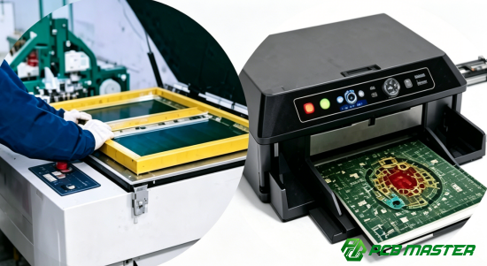
Screen printing is a stencil-based physical transfer process, while inkjet printing is a digital, maskless deposition process controlled by CAD data.
In PCB manufacturing, both screen printing and inkjet printing are used to apply functional layers such as solder mask, solder paste, and legend ink. The key difference lies in how the material is applied to the board.
- Screen printing relies on a physical stencil and pressure-based transfer
- Inkjet printing uses digital nozzles to deposit material directly onto the PCB surface
- Both are widely used in PCB production, but serve different manufacturing needs
From PCBMASTER’s production experience, screen printing is typically chosen for stable, high-volume production, while inkjet printing is more common in flexible, fast-turnaround projects.
How PCB screen printing works in solder mask and legend applications
PCB screen printing transfers solder mask or ink onto a PCB through a stencil or mesh screen using mechanical pressure.
In screen printing, a stencil or fine mesh screen is aligned on top of the PCB. Solder mask, solder paste, or legend ink is then pushed through the open areas using a squeegee.
Key process steps:
- Place stencil over the PCB and align precisely
- Apply solder mask or ink on the stencil surface
- Use a squeegee to force material through openings
- Remove stencil and cure the printed layer
This method is widely used in SMT (Surface Mount Technology) production lines because it is stable and efficient once the setup is completed. It is especially suitable for large-scale manufacturing where consistency is critical.
Real-world example:
- In consumer electronics assembly, screen printing is used for solder paste application before component placement, ensuring uniform solder joints across thousands of boards.
From PCBMASTER’s perspective, screen printing remains the preferred solution for stable mass production PCB manufacturing, particularly in automotive, industrial control, and power electronics, where process reliability is essential.
How PCB inkjet printing works in additive PCB manufacturing
Inkjet printing deposits solder mask or ink directly onto the PCB using digitally controlled nozzles without needing a stencil.
Inkjet PCB printing is a fully digital, maskless process. The print head moves across the board and ejects tiny droplets of material exactly where required.
Key process flow:
- Import PCB design from CAD/CAM system
- Convert design into digital printing instructions
- Inkjet nozzles deposit solder mask or ink layer by layer
- Material is cured after deposition
Main characteristics:
- No stencil or tooling required
- Direct control from design files
- High adaptability for frequent design changes
Practical example:
- In PCB prototyping environments, engineers can modify a trace or pad layout and immediately reprint a new board without waiting for stencil fabrication.
PCBMASTER insight:
- Inkjet printing is best suited for rapid prototyping, small batch production, and frequent design iteration, where speed and flexibility are more important than maximum throughput.
Key process differences between screen printing and inkjet printing
Screen printing uses physical stencils and is optimized for scale, while inkjet printing uses digital deposition and is optimized for flexibility.
Core process comparison
- Screen printing: physical stencil + mechanical pressure transfer
- Inkjet printing: digital nozzle + non-contact material deposition
Workflow differences
- Screen printing requires stencil fabrication before production
- Inkjet printing uses CAD files directly with minimal setup time
Production characteristics
Screen printing:
- Best for long, stable production runs
- Higher initial setup effort but low unit cost
Inkjet printing:
- Best for short runs and fast design changes
- Minimal setup, but lower throughput
Material and efficiency differences
Screen printing:
- Slightly higher material waste due to stencil coating and cleaning
Inkjet printing:
- Precise deposition reduces material waste significantly
From PCBMASTER’s real manufacturing experience, screen printing remains dominant in high-volume production environments, while inkjet printing is increasingly valuable in agile development and fast iteration workflows.
What are the advantages of screen printing in PCB manufacturing?
Screen printing is highly efficient, stable, and cost-effective, making it ideal for large-scale PCB manufacturing where consistency and low unit cost are critical.
Screen printing is one of the most widely used processes in PCB solder mask printing and solder paste application. Its main advantage is that it becomes extremely efficient once the setup is complete. For manufacturers handling large orders, this process delivers strong stability and predictable output.
From PCBMASTER’s production experience, screen printing is especially valuable when production demand is high and product design is stable over time.
Why screen printing is ideal for high-volume PCB production
Screen printing is ideal for high-volume PCB manufacturing because it offers fast cycle times, stable output, and efficient mass production after initial setup.
Once the stencil is prepared and aligned, screen printing can run continuously with very fast cycle times. This makes it suitable for high-volume PCB assembly lines, where thousands of identical boards must be produced daily.
Key advantages in high-volume production:
- Extremely fast printing cycle once stencil setup is finished
- Stable and repeatable output across large batches
- Well-suited for automated SMT production lines
Real-world example:
- In consumer electronics manufacturing (such as routers or power supplies), screen printing is used to apply solder paste to thousands of PCBs per hour with minimal variation.
PCBMASTER recommendation:
- Based on industrial production experience, screen printing is the best choice for automotive PCB manufacturing and industrial control PCBs, where long-term stability and consistent quality are critical.
How screen printing ensures consistent thickness and reliability
Screen printing ensures consistent thickness and reliability by using controlled stencil openings that deliver uniform material deposition across every PCB.
In screen printing, the stencil controls how much solder mask or solder paste is applied. Because the openings are fixed, the material thickness remains consistent from board to board.
Key points:
- Uniform solder mask and solder paste application across all PCBs
- High repeatability in SMT assembly processes
- Reduced risk of uneven coating or missing pads
Why this matters:
- Consistent thickness improves solder joint quality during reflow soldering
- Reliable coating reduces electrical defects and mechanical stress failures
Simple example:
- If solder paste thickness varies too much, components may shift or create weak solder joints. Screen printing reduces this risk by keeping deposition consistent.
From PCBMASTER’s perspective, this consistency is one of the main reasons screen printing remains widely used in mass production PCB manufacturing, especially where failure rates must be extremely low.
Why screen printing reduces unit cost in mass production
Screen printing reduces unit cost because it spreads stencil cost over large volumes and minimizes per-board material usage.
Although screen printing requires an initial investment in stencil creation, this cost becomes very small when distributed across thousands or millions of boards. As production volume increases, the cost per PCB drops significantly.
Key cost advantages:
- Reusable stencils lower long-term tooling cost
- High-speed production reduces labor time per board
- Efficient material transfer reduces wasted solder mask or paste
Material efficiency:
- Screen printing applies material in controlled layers, reducing excess usage
- Less waste compared to over-deposition or correction processes
Cost comparison example:
- Small batch production → higher cost per board due to stencil setup
- Large batch production → very low cost per board due to scale efficiency
PCBMASTER insight:
- For long production runs such as industrial controllers, automotive modules, and power electronics, screen printing provides the most cost-efficient PCB manufacturing solution while maintaining stable quality over time.
What are the disadvantages of screen printing in PCB production?
Screen printing has limited flexibility, longer setup requirements, and reduced precision for fine-pitch PCB designs, making it less suitable for rapid iteration and advanced HDI boards.
Although PCB screen printing in solder mask and solder paste application is widely used in mass production, it has clear limitations when product designs become more complex or frequently updated. From PCBMASTER’s manufacturing experience, these disadvantages are most visible in prototyping, high-density interconnect (HDI) designs, and fast-changing product cycles.
Why screen printing has limited flexibility for design changes
Screen printing is not flexible because every design change requires a new stencil, making it slow for iterative PCB development.
In screen printing, the stencil defines the exact pattern of solder mask or solder paste. If the PCB layout changes, even slightly, a new stencil must be manufactured before production can continue.
Key limitations:
- Requires a new stencil for every PCB design revision
- Not suitable for frequent layout updates or iterative engineering changes
- Each design change adds extra preparation time and cost
Real-world example:
- In PCB prototyping for IoT devices, engineers often adjust pad sizes or routing multiple times. With screen printing, each update means waiting for a new stencil, slowing down development cycles.
PCBMASTER note:
- From practical production experience, this limitation significantly increases lead time in PCB prototyping stages, making screen printing less suitable for early-stage product development.
How setup time affects production efficiency
Screen printing requires significant setup time due to stencil fabrication and alignment, which reduces efficiency for small or frequently changing production runs.
Before production starts, several setup steps are required:
- Fabrication of the stencil based on PCB design
- Precise alignment of stencil with PCB pads
- Calibration of pressure and squeegee settings
These steps ensure accuracy but take time, especially for new designs.
Key efficiency impacts:
- Higher initial setup time compared to digital PCB printing methods
- Increased preparation cost before mass production begins
- Lower efficiency for short production runs or urgent orders
Simple comparison:
- Screen printing: setup first, then fast mass production
- Inkjet printing: minimal setup, immediate production after file upload
PCBMASTER insight:
- In high-mix, low-volume manufacturing environments, setup time becomes a bottleneck, reducing overall production flexibility.
Where screen printing struggles with fine-pitch designs
Screen printing has limitations in fine-pitch and HDI PCB designs due to stencil accuracy constraints, which can lead to misalignment or uneven material deposition.
As PCB technology evolves toward high-density interconnect (HDI) and ultra-fine pitch components, the physical stencil in screen printing becomes a limiting factor.
Main technical challenges:
- Difficulty achieving ultra-fine trace and pad precision
- Risk of solder mask smudging in very small geometries
- Potential misalignment between stencil openings and PCB pads
Practical impact:
- In fine-pitch BGA components, even slight misalignment can cause solder bridging or open circuits
- Complex HDI boards require tighter tolerances than traditional screen printing can reliably support
Real-world example:
- Advanced smartphone motherboards often require extremely dense routing. In these cases, inkjet or laser-based methods may be preferred over screen printing for certain layers.
PCBMASTER perspective:
- While screen printing remains reliable for standard PCB designs, its limitations become more noticeable in advanced HDI PCB manufacturing and ultra-fine pitch applications, where digital deposition technologies offer better precision control.
What are the advantages of inkjet printing in PCB manufacturing?
Inkjet printing offers high flexibility, fast prototyping capability, and low material waste, making it ideal for rapid PCB development and small-batch production.
Inkjet printing is a digital, maskless PCB manufacturing process where solder mask or functional ink is deposited directly onto the board using controlled nozzles. Unlike traditional methods, it does not require physical tooling, which makes it highly adaptable.
From PCBMASTER’s production experience, inkjet printing is most valuable in environments where design changes are frequent and speed is critical.
Why inkjet printing is better for rapid prototyping and iteration
Inkjet printing is ideal for rapid prototyping because it eliminates stencil fabrication and allows immediate production based on digital PCB files.
In traditional PCB screen printing, a stencil must be created before production. In contrast, inkjet printing uses CAD/CAM data directly, allowing engineers to move from design to production almost instantly.
Key advantages for prototyping:
- No stencil or physical tooling required
- Immediate printing after CAD file upload
- Fast design change implementation without delays
Real-world example:
- In IoT device development, engineers often modify pad sizes, trace widths, or component placement. With inkjet PCB printing, a new version can be produced the same day for testing.
PCBMASTER insight:
- Inkjet printing significantly shortens PCB prototyping lead time, making it highly effective for R&D centers and fast product development cycles.
How inkjet printing improves design flexibility and customization
Inkjet printing improves flexibility by allowing direct digital control of each PCB layer, enabling fast customization and multi-variant production.
Because inkjet printing is fully digital, each board design is controlled by software rather than physical tools. This makes it easy to switch between designs or customize individual PCBs.
Key flexibility advantages:
- Supports instant switching between different PCB designs
- Enables variable data printing (different markings on each board)
- Ideal for multi-product or customized PCB production runs
Practical example:
- In smart home device manufacturing, different firmware versions may require different markings or slight layout changes. Inkjet printing allows these variations without changing hardware setup.
PCBMASTER perspective:
- This technology is especially useful for custom PCB manufacturing and low-volume PCB assembly, where flexibility is more important than mass-production speed.
Why inkjet printing reduces material waste in PCB processes
Inkjet printing reduces material waste by depositing only the required amount of solder mask or ink directly onto the PCB surface.
Unlike screen printing, which applies material across a stencil area, inkjet printing uses an additive, precision-based approach. This means material is only placed where it is needed.
Key waste-reduction advantages:
- No excess material outside target areas
- No stencil cleaning waste or leftover ink loss
- More efficient use of solder mask and conductive inks
Simple comparison:
- Screen printing: may apply more material than necessary, requiring cleanup
- Inkjet printing: applies micro-droplets precisely, reducing overuse
Real-world example:
- In small-batch PCB production for wearable devices, inkjet printing reduces expensive specialty ink consumption, lowering overall production cost per design iteration.
PCBMASTER insight:
- This efficiency makes inkjet printing a strong option for environmentally conscious PCB manufacturing and cost-sensitive prototype production.
What are the disadvantages of inkjet printing in PCB production?
Inkjet printing is less suitable for high-volume production, may face material compatibility issues, and is still less mature in global industrial PCB manufacturing compared to screen printing.
While inkjet PCB printing technology offers strong advantages in flexibility and prototyping, it is not always the best choice for large-scale industrial production. From PCBMASTER’s manufacturing experience, its limitations become more obvious when production volume, long-term stability, and standardized processes are required.
Why inkjet printing is slower for high-volume manufacturing
Inkjet printing is slower than screen printing because it has lower throughput and is not designed for large-scale SMT production lines.
Inkjet printing works by depositing tiny droplets of material one layer at a time. While this improves precision, it also reduces speed compared to traditional PCB screen printing processes.
Key limitations:
- Lower throughput compared to stencil-based screen printing
- Not optimized for continuous, high-speed SMT assembly lines
- Printing time increases significantly for large PCB batches
Real-world example:
- In consumer electronics factories producing thousands of PCBs per hour, screen printing is preferred because inkjet printing cannot match the same production speed.
PCBMASTER insight:
- Inkjet printing is best suited for low to medium volume PCB manufacturing, not for mass production environments where speed and scalability are critical.
How inkjet printing may face material and adhesion challenges
Inkjet printing can face challenges with ink compatibility and adhesion stability, especially when different PCB materials or curing conditions are involved.
Inkjet PCB printing relies on specialized conductive inks or solder mask materials that must match the PCB substrate. If material selection is not optimized, performance issues may occur.
Key technical challenges:
- Requires compatible inks for different PCB materials (FR4, flexible PCB, HDI substrates)
- Adhesion strength may vary depending on surface treatment and curing process
- Inconsistent curing can affect long-term durability
Simple explanation:
- If the ink does not “stick” properly to the board, it may peel or degrade during soldering or thermal cycling.
Real-world example:
- In harsh environments like automotive electronics, poor adhesion can lead to coating failure after repeated temperature changes.
PCBMASTER perspective:
lCareful material selection and process tuning are required to ensure reliable results in inkjet PCB manufacturing, especially for industrial-grade applications.
Where inkjet printing may lack long-term industrial maturity
Inkjet printing is still less standardized and more equipment-sensitive than screen printing, which limits its widespread use in long-term industrial PCB production.
Compared to mature PCB screen printing technology, inkjet printing is still evolving in terms of global standardization and industrial adoption.
Main limitations:
- Less standardized process across global PCB fabs
- Different equipment brands may produce different results
- Higher sensitivity to maintenance and calibration conditions
Operational challenges:
- Nozzle clogging or misalignment can affect print quality
- Requires frequent calibration for stable performance
- Maintenance costs can be higher due to precision components
Real-world example:
- Some PCB factories report inconsistent results when switching between inkjet systems from different suppliers, requiring additional process tuning.
PCBMASTER insight:
- While inkjet printing is rapidly developing, it is currently more suitable for R&D, prototyping, and flexible manufacturing environments rather than fully standardized mass production lines.
How do screen printing and inkjet printing compare in PCBMASTER’s manufacturing experience?
From PCBMASTER’s production experience, screen printing is best for stable, high-volume PCB manufacturing, while inkjet printing is better for flexible, low to medium-volume production and rapid prototyping.
In real PCB manufacturing environments, these two technologies are not direct competitors but complementary processes used at different stages of product development. Screen printing dominates in mature, large-scale SMT production lines, while inkjet printing is increasingly used in agile engineering and prototype workflows.
The following comparison table summarizes PCBMASTER’s practical experience across key manufacturing dimensions:
| Dimension | Screen Printing | Inkjet Printing |
| Production Volume | Best for high-volume manufacturing | Best for low to medium volume |
| Setup Time | High (stencil required) | Very low (digital file-based) |
| Cost Efficiency | Excellent at scale | Higher per unit cost |
| Flexibility | Low (needs stencil changes) | Very high (CAD-driven) |
| Precision | Stable and mature | High for fine customization |
| Material Waste | Moderate | Low (additive process) |
| Best Use Case | Mass production, automotive PCB | Prototyping, R&D, custom PCB |
Cost comparison between screen printing and inkjet printing
Screen printing is more cost-effective in large-scale production, while inkjet printing is more cost-efficient for small batches and prototype runs.
In PCB screen printing manufacturing, the main cost comes from stencil creation, but this cost is spread across large production volumes. Once production starts, the cost per PCB becomes very low.
Key cost characteristics:
- Screen printing:- Lower unit cost at high volume- High efficiency after initial setup- Best for long production runs (10,000+ units)
- Inkjet printing:- No stencil cost, but higher equipment and ink cost per unit- More economical for small batches or prototype runs- Avoids tooling cost for each design change
Real-world example:
- Automotive PCB production (high volume): screen printing significantly reduces per-unit cost
- Prototype IoT PCB development: inkjet printing avoids repeated stencil expenses during design changes
PCBMASTER insight:
- In cost-sensitive mass production PCB manufacturing, screen printing remains the dominant solution, while inkjet printing supports flexible development cycles.
Quality and precision comparison in real production cases
Screen printing delivers highly consistent bulk production quality, while inkjet printing provides better adaptability for fine adjustments and design-specific precision.
In terms of PCB manufacturing quality control, screen printing is known for its stability. The stencil ensures consistent solder paste or solder mask thickness across thousands of boards.
Key quality characteristics:
- Screen printing:- Highly consistent solder paste deposition- Stable performance in SMT assembly processes- Low variation between batches
- Inkjet printing:- High adaptability for fine design adjustments- Good for selective or variable deposition- More suitable for complex or customized layouts
Real-world example:
- In mass production of power supply PCBs, screen printing ensures uniform solder joints, reducing defect rates
- In prototype HDI PCB testing, inkjet printing allows quick adjustments to pad or trace modifications
PCBMASTER perspective:
- Screen printing is preferred for repeatable industrial PCB quality, while inkjet printing is better for engineering flexibility and design refinement stages.
Production scalability comparison for industrial PCB orders
Screen printing is optimized for large-scale industrial PCB production, while inkjet printing is optimized for prototyping and agile, small-batch manufacturing.
Scalability is a key factor in PCB manufacturing process selection. Screen printing is designed for continuous, high-speed production lines, making it ideal for large industrial orders.
Key scalability differences:
- Screen printing:- High throughput suitable for thousands to millions of units- Stable integration with SMT production lines- Efficient for long-term product manufacturing
- Inkjet printing:- Better suited for small batch or on-demand production- Flexible scaling based on design changes- Slower when production volume increases
Simple comparison:
- Screen printing = “factory mass production mode”
- Inkjet printing = “agile development and prototype mode”
Real-world example:
- Consumer electronics factories use screen printing for full production runs
- R&D departments use inkjet printing to validate new PCB designs before mass production
PCBMASTER insight:
- For industrial PCB orders requiring stable long-term supply, screen printing remains the most scalable and reliable solution, while inkjet printing supports innovation and early-stage product development.
When should you choose screen printing or inkjet printing for PCB projects?
Screen printing should be used for stable, high-volume PCB manufacturing, while inkjet printing is better for prototyping, customization, and low-volume production with frequent design changes.
Choosing between PCB screen printing and inkjet printing depends mainly on production stage, order volume, and design stability. From PCBMASTER’s manufacturing experience, the key decision factor is whether the PCB design is already stable or still evolving.
Screen printing is optimized for repeatable industrial production, while inkjet printing is designed for flexibility and fast iteration during early development.
Best scenarios for using screen printing in PCB production
Screen printing is best used in high-volume, stable, and long-life PCB manufacturing where consistency and low cost per unit are the top priorities.
High-volume consumer electronics
Screen printing is widely used in mass production PCB assembly for consumer electronics such as routers, power adapters, and household devices. Once the stencil is ready, thousands of identical boards can be produced quickly with stable quality.
Automotive and power electronics
In automotive PCB manufacturing and power electronics systems, reliability is critical. Screen printing ensures consistent solder paste and solder mask thickness, reducing failure risk in harsh environments such as heat and vibration.
Long-term stable product lines
For products with long lifecycle stability, screen printing is ideal because the design does not change frequently. This avoids repeated stencil costs and keeps production efficient over time.
PCBMASTER insight:
- Screen printing is recommended when the PCB design is finalized and production volume is predictable and large.
Best scenarios for using inkjet printing in PCB production
Inkjet printing is best for early-stage development, small batch production, and customized PCB designs that require frequent changes.
Rapid prototyping and R&D
In PCB prototyping and R&D environments, inkjet printing allows engineers to quickly test new designs without waiting for stencil fabrication. Changes can be applied directly through CAD files.
Custom PCB designs and low-volume orders
For custom PCB manufacturing or low-volume PCB assembly, inkjet printing avoids tooling costs and supports fast delivery for specialized products.
Multi-variant smart devices
In industries like IoT and smart devices, different product versions may require slight design changes. Inkjet printing supports multi-variant PCB production, where each board can be slightly different without extra setup cost.
PCBMASTER insight:
- Inkjet printing is most effective when speed and design flexibility are more important than large-scale production efficiency.
PCBMASTER recommendation for hybrid manufacturing strategies
PCBMASTER recommends using inkjet printing for prototyping and screen printing for mass production to achieve the best balance of speed, cost, and scalability.
Use inkjet for prototyping → screen printing for mass production
A practical hybrid PCB manufacturing strategy is to start with inkjet printing during the design phase. Once the design is finalized and stable, transition to screen printing for large-scale production.
Workflow example:
- Inkjet printing for early PCB prototypes and design testing
- Design optimization based on test results
- Screen printing for full-scale production rollout
Optimize cost, speed, and design flexibility across product lifecycle
This combined approach helps manufacturers:
- Reduce development time in early stages
- Avoid unnecessary stencil costs during iteration
- Achieve low unit cost in final mass production
- Maintain flexibility without sacrificing scalability
PCBMASTER perspective:
- This hybrid PCB production strategy is widely used in modern electronics manufacturing to balance innovation speed and industrial efficiency, especially in fast-moving industries like consumer electronics, automotive electronics, and IoT devices.
Conclusion
Screen printing and inkjet printing each play an important role in modern PCB manufacturing, but they are designed for different production goals. Screen printing remains the preferred solution for high-volume, stable production because of its speed, consistency, and low unit cost. In contrast, inkjet printing offers greater flexibility, faster design iteration, and better adaptability for prototyping and customized PCB projects.
As PCB technologies continue to evolve toward higher complexity and shorter development cycles, manufacturers must choose the process that best matches their production requirements, budget, and scalability expectations. In many cases, combining both technologies can provide the best balance between development flexibility and manufacturing efficiency.
Drawing on extensive PCB and PCBA production experience, PCBMASTER helps customers select the most suitable printing process based on real project demands, whether for rapid prototyping, industrial electronics, automotive applications, or large-scale commercial production. By aligning the right technology with the right stage of production, manufacturers can improve quality, reduce costs, and accelerate product delivery more effectively.
FAQ – Screen Printing vs Inkjet Printing in PCB Manufacturing
Is inkjet printing replacing screen printing in PCB manufacturing?
No. Screen printing and inkjet printing currently coexist because they serve different PCB manufacturing needs.
Screen printing is still the dominant choice for high-volume PCB production due to its speed, stability, and low cost per unit. Inkjet printing, however, is becoming increasingly popular in PCB prototyping, R&D, and customized production because it offers higher flexibility and faster design changes.
From PCBMASTER’s manufacturing experience:
- Screen printing is better for stable, large-scale production lines
- Inkjet printing is better for fast iteration and low-volume manufacturing
Rather than replacing each other, the two technologies are often used together at different stages of PCB production.
Which printing method is more cost-effective for PCB production?
Screen printing is more cost-effective for mass production, while inkjet printing is more economical for low-volume and prototype PCB manufacturing.
The cost advantage depends mainly on production quantity.
- Screen printing: - Requires stencil fabrication - Lower cost per PCB in large production runs - Best for long-term, high-volume manufacturing
- Inkjet printing: - No stencil required - Reduces tooling cost for small batches - Better for frequent design revisions
Example:
- Producing 100 prototype PCBs → inkjet printing is usually cheaper
- Producing 100,000 automotive PCBs → screen printing is far more economical
PCBMASTER recommends selecting the process based on expected production scale and design stability.
Can inkjet printing achieve the same precision as screen printing?
Yes, inkjet printing can achieve very high precision in some applications, but it is generally slower than screen printing in large-scale production.
Inkjet printing uses digitally controlled nozzles to place material precisely onto the PCB surface. This allows excellent control for:
- Fine adjustments
- Selective deposition
- Complex customized patterns
However, screen printing still offers advantages in:
- High-speed consistency
- Large-volume repeatability
- Mature industrial process stability
PCBMASTER insight:
- Inkjet printing may outperform screen printing in certain fine-feature applications, but screen printing remains more practical for large-scale industrial manufacturing.
Which method is better for HDI and fine-pitch PCB designs?
Inkjet printing offers better flexibility for complex HDI designs, while advanced screen printing is still widely used in high-volume HDI PCB manufacturing.
HDI (High-Density Interconnect) PCBs require very small pads, fine traces, and tight spacing. Inkjet printing helps by enabling:
- Precise digital deposition
- Fast design modifications
- Reduced tooling limitations
However, modern screen printing technology has also improved significantly and continues to dominate mass-production HDI PCB assembly because of its:
- Faster throughput
- Stable process control
- Better scalability for industrial production
PCBMASTER perspective:
- Inkjet printing is highly useful during HDI prototyping and design optimization, while screen printing remains the preferred option for mature HDI products entering large-scale production.
What does PCBMASTER recommend for mixed production environments?
PCBMASTER recommends combining inkjet printing and screen printing based on the product lifecycle stage.
A hybrid manufacturing strategy often delivers the best overall results.
Typical workflow:
- Use inkjet printing during prototyping and R&D
- Quickly modify and validate PCB designs
- Switch to screen printing after design stabilization
- Scale production efficiently for commercial manufacturing
Main benefits:
- Faster development cycles
- Lower prototyping cost
- Improved manufacturing scalability
- Better balance between flexibility and production efficiency
From PCBMASTER’s experience, this combined approach is especially effective for industries with fast product updates, including consumer electronics, automotive electronics, and IoT device manufacturing.
About the Author

Carol Luo
PCB Design EngineerI'm Carol, a PCB Engineer at PCBMASTER with experience in PCB design and manufacturing engineering since 2018. I focus on translating engineering requirements into reliable PCB solutions, with expertise in stack-up design, material selection, and design-for-manufacturing (DFM). I share practical engineering insights from real-world PCB design and production experience.
Visit Carol Luo's Profile