


Blind Via vs. Buried Via in PCB Design: Differences and Design Considerations
Designing high-density PCBs requires smart use of vias to save space and maintain performance. Blind vias and buried vias are two common types that connect different layers without disrupting the overall board layout. Understanding the differences between them is key to efficient PCB design.
Blind vias connect an outer layer to one or more inner layers, making them ideal for compact boards like smartphones and wearable devices. In contrast, buried vias connect only internal layers, leaving the outer surfaces free for routing. This approach is commonly used in complex multi-layer boards for industrial or aerospace applications.
This guide from PCBMASTER explains the characteristics, applications, and selection considerations for both via types. With clear examples and practical professional advice, it aims to help designers optimize board space, maintain signal integrity, and simplify PCB layout decisions.
What Is a Blind Via and How Is It Used in PCB Design?
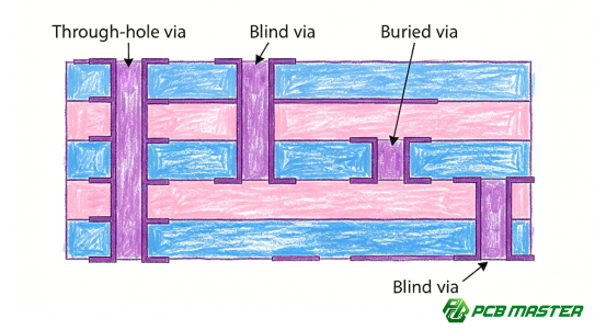
A blind via is a hole in a printed circuit board (PCB) that connects an outer layer to one or more inner layers without going through the entire board. It allows designers to save space, route signals efficiently, and build high-density boards.
Definition and Characteristics of Blind Vias
Blind vias are vertical connections that link an outer PCB layer to internal layers only. Unlike through-hole vias, they do not pass completely through the board. This design saves valuable space on outer layers, making it easier to place components or traces.
Key characteristics include:
l Layer connection: Only connects surface layer(s) to specific inner layer(s).
l Aspect ratio and depth: The depth of the via compared to its diameter is limited, often not exceeding 10:1, to ensure proper plating and electrical performance.
l Manufacturing technique: Most blind vias in modern PCBs are created using laser drilling for precise small holes, especially in high-density boards.
Example: A smartphone PCB often uses blind vias to connect outer routing layers to internal power planes, reducing clutter and leaving more room for miniaturized components.
Common Applications of Blind Vias
Blind vias are essential for high-density interconnect (HDI) PCBs, where saving space is critical.
l Mobile devices and laptops: Their compact boards require many signals in a small area. Blind vias allow designers to route multiple layers without increasing PCB size.
l Compact electronics: Wearable devices, cameras, and small IoT devices use blind vias to maintain small form factors.
l Minimal routing disruption: In boards where outer layers need clear space for sensitive signals or components, blind vias prevent interference and maintain routing flexibility.
Case Study: On a modern smartphone motherboard, blind vias connect outer signal layers to inner power and ground layers, ensuring high-speed signals are routed without creating interference on the outer layers.
Advantages and Limitations of Blind Vias
Advantages:
l Saves PCB space: Blind vias free up outer layers for traces and components.
l Improves routing flexibility: Designers can route signals efficiently, especially in HDI boards with limited space.
l Supports miniaturization: Essential for compact electronics where board real estate is precious.
Limitations:
l Higher manufacturing cost: Requires precise laser drilling, increasing fabrication complexity.
l Depth limitations: High aspect ratios can be difficult to plate uniformly, limiting maximum via depth.
l Design complexity: Extra planning is required to integrate blind vias into layer stack-ups effectively.
Example: A wearable device PCB may require multiple blind vias to route signals under tiny surface-mounted components. While this saves space, the board manufacturer must carefully control drilling and plating to avoid defects.
What Is a Buried Via and When Should Designers Use It?
A buried via is a hole inside a PCB that connects only internal layers and does not appear on the surface. Designers use buried vias in multi-layer, high-density boards where outer layers must remain clear for routing, signal integrity, or component placement.
Definition and Characteristics of Buried Vias
Buried vias are completely embedded inside a PCB, linking only internal layers. Unlike blind vias, they are invisible from the surface and cannot be seen from either side.
Key characteristics include:
l Internal layer connection: Only connects two or more inner layers, leaving outer layers untouched.
l Fully embedded: Since buried vias do not reach the surface, they do not interfere with component placement or outer-layer routing.
l Manufacturing process: Creating buried vias requires sequential lamination, where inner layers are drilled and plated before the rest of the board layers are laminated.
Example: In a 12-layer HDI PCB for industrial control equipment, buried vias connect inner power and ground planes, while the outer layers remain free for high-speed signal traces.
Common Applications of Buried Vias
Buried vias are widely used in complex, high-performance PCBs, especially when outer layers need to remain open.
l Multi-layer HDI boards: Buried vias allow designers to connect internal layers without consuming space on surface layers.
l Industrial and aerospace electronics: Boards in these sectors often require clean outer layers for reliability and precise routing of high-speed signals.
l Complex stack-ups: Buried vias help isolate signals in sensitive layers, reducing interference and maintaining signal integrity.
Case Study: An aerospace communication PCB uses buried vias to connect inner signal layers while keeping the outer layers available for shielding and high-speed traces. This prevents crosstalk and reduces electromagnetic interference (EMI).
Advantages and Limitations of Buried Vias
Advantages:
l Keeps outer layers clean: Buried vias do not appear on the board surface, leaving space for critical routing or component placement.
l Supports high layer counts: Essential for multi-layer HDI PCBs where multiple internal planes must interconnect.
l Improves signal integrity: By isolating signals inside the PCB stack, buried vias reduce interference from outer-layer routing.
Limitations:
l Increased manufacturing complexity: Sequential lamination is required, making production more difficult and costly.
l Time-consuming process: Building layers with buried vias adds steps to PCB fabrication, increasing lead times.
l Design planning required: Designers must carefully plan layer stack-ups to ensure buried vias do not interfere with other internal connections.
Example: A high-speed server motherboard with 14 layers uses buried vias to connect internal voltage planes. Although manufacturing is more expensive and complex, the design achieves high performance without crowding outer signal layers.
What Are the Main Differences Between Blind and Buried Vias?
The main differences between blind and buried vias lie in layer connectivity, visibility on the PCB surface, manufacturing complexity, cost, and typical applications. Understanding these differences helps PCB designers select the right via type for their project.
Layer Connectivity
Blind and buried vias connect different PCB layers, and this affects their function and design flexibility.
l Blind vias connect an outer layer to one or more inner layers, allowing signals or power to pass from the surface to internal planes without going through the entire board.
l Buried vias connect only inner layers, fully hidden inside the PCB. This is useful when designers need internal routing without affecting the outer layers.
Example: In a smartphone PCB, blind vias link the top signal layer to an inner power plane, while buried vias connect internal ground and power planes without touching the outer routing layers.
Visibility on PCB Surface
Visibility affects component placement and outer-layer routing.
l Blind vias are visible from one side, which can slightly limit component placement on that surface.
l Buried vias are completely hidden, leaving both outer layers free for routing and components.
Practical Note: Using buried vias in high-density boards ensures that sensitive high-speed signals are not obstructed by vias on the surface, improving signal integrity.
Manufacturing Complexity and Cost
The type of via influences how difficult and costly it is to produce a PCB.
l Blind vias are simpler and faster to produce. They can be made using laser drilling or mechanical drilling, depending on the PCB’s density.
l Buried vias require sequential lamination, a multi-step process that adds both cost and lead time.
Example: A 6-layer laptop motherboard may use blind vias to simplify production, while a 12-layer industrial control PCB relies on buried vias to connect internal planes without affecting the surface layers, accepting higher manufacturing costs.
Typical Use Cases
Different applications favor one via type over the other.
l Blind vias are common in consumer electronics and compact boards, where saving outer-layer space is important but manufacturing simplicity is desired.
l Buried vias are ideal for high-density industrial boards and multi-layer high-speed circuits, where signal integrity, clean outer layers, and complex internal routing are critical.
Case Study: In wearable devices, blind vias reduce outer-layer congestion for small components. In aerospace PCBs, buried vias allow dozens of internal connections while keeping the surface free for critical high-speed routing.
Comparison Table
Feature Blind Via Buried Via Layer Connectivity Outer → Inner Inner → Inner Visibility Visible from one side Completely hidden Manufacturing Laser or mechanical drilling, simpler Sequential lamination, complex Cost & Time Moderate Higher, longer production Typical Use Cases Consumer electronics, compact boards High-density industrial boards, multi-layer HDI PCBs
| Feature | Blind Via | Buried Via |
| Layer Connectivity | Outer → Inner | Inner → Inner |
| Visibility | Visible from one side | Completely hidden |
| Manufacturing | Laser or mechanical drilling, simpler | Sequential lamination, complex |
| Cost & Time | Moderate | Higher, longer production |
| Typical Use Cases | Consumer electronics, compact boards | High-density industrial boards, multi-layer HDI PCBs |
How to Decide Between Blind and Buried Vias in Your PCB Design?
Choosing between blind and buried vias depends on space constraints, layer count, electrical performance, manufacturing capabilities, and budget. The right choice ensures the PCB meets design goals while remaining manufacturable and cost-effective.
Key Design Considerations
PCB designers must evaluate multiple factors to decide whether to use blind or buried vias in a specific board.
Space Constraints and Layer Count
l Blind vias are ideal for boards where outer layers need routing space but the total layer count is moderate.
l Buried vias are better for multi-layer PCBs with dense internal routing, where space inside the board is limited.
Example: A 6-layer smartphone PCB may use blind vias for outer-layer connections, whereas a 12-layer industrial control board uses buried vias to connect internal planes without crowding the surface.
Electrical Performance (Signal Integrity and Impedance Control)
l High-speed circuits may require buried vias to reduce interference and maintain signal integrity.
l Blind vias are sufficient for low-to-medium speed signals where minor surface layer disruption is acceptable.
Step: Designers map signal paths and identify which vias will minimize crosstalk and impedance variation.
Manufacturing Capabilities and Budget
l Blind vias are generally cheaper and faster to manufacture due to simpler drilling.
l Buried vias require sequential lamination, increasing production cost and time.
Practical Tip: Match via selection to manufacturer capabilities to avoid costly production delays.
PCBMASTER Recommendations
PCBMASTER advises designers on via selection based on project type, balancing performance, cost, and manufacturability.
Project-Based Advice
l For consumer electronics with moderate layer counts, PCBMASTER recommends blind vias to save cost and maintain outer-layer routing flexibility.
l For high-performance industrial or aerospace boards, buried vias are suggested to ensure clean outer layers and reliable multi-layer connections.
Balancing Performance, Cost, and Manufacturability
PCBMASTER recommends combining blind and buried vias when necessary.
Step-by-Step Approach:
1. Evaluate board layer count and component density.
2. Identify critical signals needing minimal interference.
3. Select blind vias where outer-layer space is tight but speed is moderate.
4. Use buried vias for inner-layer connections requiring high reliability or high-speed routing.
Example: On a compact HDI PCB for a wearable device, PCBMASTER engineers used blind vias for outer-layer signals and buried vias for power and ground planes, achieving a balance between cost and performance.
Conclusion
Choosing the right via type is a critical step in PCB design. Blind vias provide a simple, space-saving solution for outer-layer connections, perfect for compact consumer electronics. Buried vias, fully hidden inside the board, are essential for high-density, multi-layer PCBs where signal integrity and clean outer layers are required.
Understanding the differences, advantages, limitations, and applications of blind and buried vias allows designers to make informed decisions that balance performance, manufacturability, and cost. By carefully evaluating factors like board complexity, layer count, signal requirements, and budget, engineers can select the via type that best fits their project goals.
When navigating these choices, having expert guidance can make a significant difference. That’s where PCBMASTER comes in. With years of experience in advanced PCB and HDI board manufacturing, PCBMASTER helps engineers choose the right via type for every design, ensuring reliability, efficiency, and high-quality results.
FAQ About Blind and Buried Vias
Can blind and buried vias coexist on the same PCB?
Yes, blind and buried vias can coexist on the same PCB. Designers often use a combination to optimize space, signal routing, and layer connectivity. For example, blind vias may connect outer layers to inner layers, while buried vias connect internal planes without affecting the surface. This hybrid approach is common in multi-layer HDI boards to balance manufacturability and performance.
Which via type is better for high-speed signal routing?
Buried vias are generally better for high-speed signal routing because they are fully embedded inside the PCB and do not disrupt outer-layer traces. By isolating high-speed signals internally, buried vias reduce crosstalk, signal interference, and impedance variations. Blind vias can be used for moderate-speed signals but may slightly affect outer-layer routing.
Do blind and buried vias affect PCB cost significantly?
Yes, both via types can impact PCB cost, but in different ways:
l Blind vias increase cost slightly due to laser or precise mechanical drilling.
l Buried vias are more expensive because they require sequential lamination and additional manufacturing steps. Using the right via type strategically helps balance cost and performance.
Yes, each via type has practical limitations:
l Blind vias have depth-to-diameter ratios, typically not exceeding 10:1, which limits maximum PCB thickness for reliable plating.
l Buried vias are limited by the sequential lamination process and internal layer alignment, making very thick boards or extremely high layer counts more complex to manufacture.

