


PCB Assembly Delivery Type A Guide to Single Pieces vs. Panelized Boards — How to Choose the Optimal Option
Introduction
In the design and manufacturing of electronic products, a critical decision is often overlooked: choosing between single-piece or panelized PCB assembly. This choice directly impacts product cost, efficiency, and quality.
In modern electronic product manufacturing, PCB assembly is a core process. Whether it's a simple remote control or a complex smartphone, none can function without precisely and reliably assembled circuit boards.
For electronic engineers, procurement specialists, and business decision-makers, a fundamental choice arises when preparing for PCB assembly: should they use single-piece PCBs or opt for a panelized approach? This decision influences product cost, production efficiency, and quality reliability.
Introduction to PCB Assembly
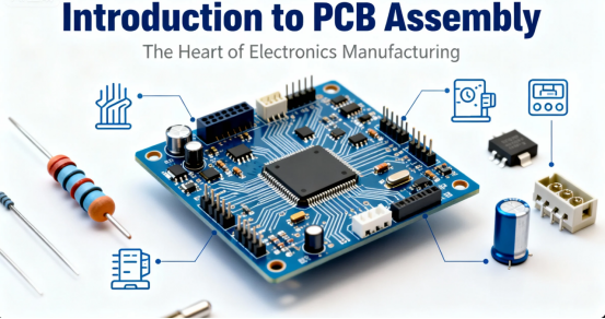
Printed circuit board (PCB) assembly is at the heart of modern electronics manufacturing, transforming bare circuit boards into fully functional devices by mounting and soldering electronic components with precision and reliability. The PCB assembly process is a multi-step journey that begins with the fabrication of the bare board and culminates in a thoroughly tested, production-ready circuit board.
The assembly process typically starts with solder paste printing, where a thin layer of solder paste is applied to the surface mount pads of the PCB. This is followed by the placement of electronic components—such as resistors, capacitors, and integrated circuits—using automated machines like pick and place machines. Once all components are in position, the board moves through a reflow oven, where the solder paste melts and forms strong, reliable solder joints, securing the components to the board.
For assemblies that require through hole components, the process may also include wave soldering or manual soldering, ensuring that all types of components are properly attached. Mixed assembly, which combines surface mount technology (SMT) and through hole assembly, is common in complex or high-reliability applications.
Quality assurance is a critical part of the PCB assembly process. Automated optical inspection (AOI) systems scan the boards for misaligned components, solder bridges, and other defects. X-ray inspection is used for hidden solder joints, such as those found in BGA package functional testing. Additional test methods, including in circuit testing, flying probe testing, and functional testing, help verify that each circuit board meets stringent performance standards. Final inspection and, if required, conformal coating, further ensure consistent quality and durability.
PCB manufacturing also involves the initial fabrication of the bare circuit boards, using processes like laser direct imaging and direct imaging to define circuit patterns. Materials such as copper, fiberglass, and ceramics are selected based on the application, and the manufacturing process includes etching, drilling, and plating to create multilayer boards and complex circuit paths.
PCB assembly services range from prototype assembly for small batches to high volume, mass production runs. Professional engineers and specialized assembly lines handle everything from component sourcing to the final assembly, offering customized services to meet diverse requirements. Whether you need a single prototype or thousands of units, choosing the right PCB assembly service is crucial for balancing cost, turnaround time, and quality.
Panelization is another key aspect of the assembly process. PCB panelization involves arranging multiple individual PCBs onto a single panel, allowing for simultaneous assembly and testing. This approach is especially beneficial for large quantities, as it streamlines the production line, reduces handling time, and improves efficiency. However, careful planning is required to determine optimal panel sizes, the arrangement of individual boards, and the best separation process—be it mechanical cutting, laser cutting, or routing—to avoid mechanical stress and ensure clean separation without compromising quality.
Ultimately, the success of any electronics manufacturing project depends on a well-designed assembly process, robust quality control, and the ability to scale from prototypes to mass production. By understanding the intricacies of PCB assembly, from solder paste inspection to final functional testing, manufacturers can achieve the best quality, cost-effective solutions for their printed circuit board needs. Whether working with individual boards or panelized assemblies, the right approach and reliable PCB assembly solutions are essential for delivering high-performance, reliable electronic products.
Single-Piece PCB Assembly: A Flexible Choice for Prototypes and Small Batches
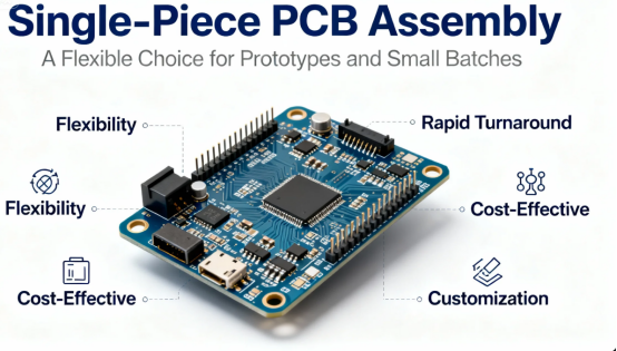
Single-piece PCB assembly, as the name suggests, involves assembling and soldering components onto individual pcb boards, which serve as the foundational element in the process. The process begins with bare boards, which are prepared for assembly. PCB fabrication is completed before assembly begins. Preparation for assembly also requires Gerber files, which guide the manufacturing and assembly of single-piece PCBs. This approach is particularly common in the early stages of product development and for small-batch production.
Advantages of Single-Piece PCBs
High Flexibility: Single-piece PCB assembly is suitable for prototype creation and design verification phases, allowing for rapid design iteration and saving development time. When designs require frequent modifications, the low-cost alteration advantage of single-piece PCBs becomes significant.
Low Cost Barrier: For small orders, single-piece PCB assembly avoids the extra costs associated with panelization, such as process rails, V-cuts, or break-away tabs, resulting in lower initial investment.
Faster Delivery: Producing single-piece PCBs with simple structures often has shorter lead times, and the overall process from order placement to assembly completion is more straightforward.
Limitations of Single-Piece PCBs
Lower Production Efficiency: For mass production, processing single boards sequentially is significantly less efficient than processing multiple panels simultaneously. SMT equipment cannot fully utilize its high-speed capabilities with small, individual boards.
Challenging Consistency: In multi-batch, single-piece PCB assembly, the need for repeated positioning and clamping can increase the risk of quality variations.
Cost Inefficiency: For larger order quantities, the unit cost of single-piece PCBs is higher than for panelized boards. This is especially true in SMT processing, where small individual boards might encounter "minimum placement fees."
Panelized PCB Assembly: An Efficient Solution for Mass Production
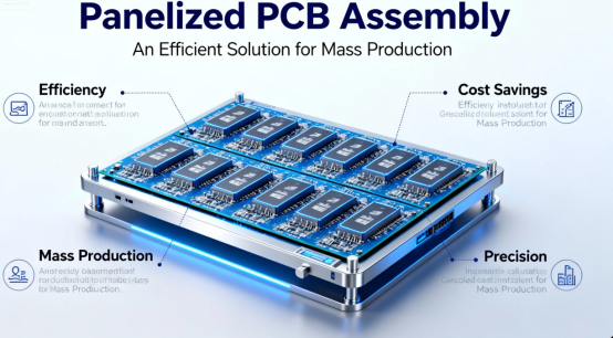
Panelized PCBs involve combining multiple identical or different individual PCBs onto a larger panel, commonly referred to as a pcb panel, for unified assembly. Panelized assembly is typically performed on an automated assembly line, which streamlines the process and increases efficiency by allowing multiple printed circuit boards to be processed together. Optimizing pcb panel layout improves handling, component placement, and depaneling efficiency. During printed circuit board assembly, pick and place machines are used for high-speed, precise component placement on all boards in the panel, relying on accurate smt pads for reliable results. The comprehensive production processes include solder paste application, automated placement, reflow soldering to secure components, and final inspection. This approach results in multiple pcb assemblies being produced simultaneously, improving throughput. Turnkey panelized assembly services can include all the materials required, from electronic components to bare PCBs, further simplifying the process.
Main Panelization Methods
V-Scoring: V-shaped grooves are pre-cut between the boards. After assembly, the boards are separated by breaking them apart along these grooves. This method suits boards with straight edges, resulting in relatively clean separation edges.
Tab Routing (Mouse Bites): Small perforations (like stamp holes) are created in the connecting bridges between boards. After assembly, the boards are broken apart at these perforated tabs. This method is suitable for PCBs with irregular shapes.
Solid Tab Panelization: Boards are connected by solid tabs (bridges) and separated by depaneling routers after assembly. This provides stronger mechanical support, making it suitable for PCBs with heavier components.
Significant Advantages of Panelized PCBs
Greatly Enhanced Production Efficiency: Panelization allows SMT equipment to process multiple circuit boards in one go, significantly improving equipment utilization and production speed. Continuous operation on a panel reduces the time wasted on loading and unloading individual boards.
Clear Cost Benefits: By optimizing material utilization, panelization reduces material waste and lowers the unit cost. For bulk orders, panelized production avoids the "minimum SMT placement fee" often applied to small individual boards.
Better Quality Consistency: Panels provide better positioning references for SMT processes. Process rails can be added to include tooling holes and fiducial marks, facilitating optical positioning and handling by SMT machines, thereby improving placement accuracy and efficiency.
Simplified Subsequent Processes: Panelized boards also streamline subsequent steps like cleaning, testing, and packaging. Standardized panel sizes are easier to handle in automated equipment.
Challenges of Panelized PCBs
Higher Initial Cost: Panelization requires designing the connection methods, adding process rails, etc., increasing upfront design and material costs.
Added Separation Step: An additional depaneling step is required after assembly is complete, such as breaking V-scored panels, snapping tab-routed boards, or routing.
Increased Design Complexity: Panel design must consider connection strength, safe distances between components and board edges, and the impact of the separation method on components.
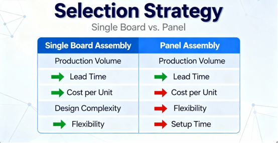
Selection Strategy: Single Board vs. Panel
Key Considerations
Order Quantity: This is the most direct deciding factor. Small batches (typically under 50 units) are more suitable for single PCBs, while larger orders are more economical with panels.
Board Size and Shape: Very small PCBs (with any side less than 30mm) are strongly recommended for panelized assembly; otherwise, SMT efficiency is extremely low.
Component Layout: If components are placed too close to the board edge (less than 3mm), process rails need to be added during panelization to ensure placement accuracy.
Budget Constraints: Single PCBs can save upfront costs when the budget is tight and quantities are low.
Product Stage: The design verification phase suits single PCBs, while the mass production phase suits panels.
Practical Selection Guide
Based on industry experience, we can summarize the following selection guide:
·Prototype Development: Choose single PCBs for quick modifications and verification.
·Small-Batch Production (<50 units): Prioritize single PCBs, unless the board size is exceptionally small.
·Medium to Large Batch Production (≥50 units): Strongly recommend panelization to significantly reduce costs and improve efficiency.
·Unconventional Board Shapes: Panelization is often the better choice, improving material utilization through optimized layout.
Best Practices for Panel Design
A successful panel design must consider the following key factors:
Clearance: Maintain a distance of ≥0.4mm between the V-score centerline and nearby traces or copper pours. For tab routing, keep a distance of ≥0.2mm between the perforations and traces/copper.
Process Rails Design: Add process rails around the panel perimeter, typically 5mm wide (minimum 3mm). These rails should include tooling holes (generally 2mm unplated holes) and fiducial marks.
Component Orientation: Orient all individual boards on the panel consistently where possible to facilitate SMT machine operation.
Future Trends in PCB Assembly Delivery Types

As electronic products evolve toward miniaturization and higher performance, PCB assembly technologies are also advancing. Flexible Panelization Services are becoming more common, such as the free panelization services offered by manufacturers like JLCPCB.
Design-for-Manufacturability (DFM) Integration is optimizing workflows. Intelligent DFM tools can predict panelization outcomes during the design stage, identifying and mitigating production risks early on.
Conclusion
Choosing the right PCB delivery type is akin to selecting a shipping method — single-piece delivery suits urgent, small items, while panelized shipping is for bulk goods. The fundamental principle, "Small batches favor single boards; large batches favor panels," can guide you toward the most suitable solution among the many options.
Regardless of the chosen method, close communication with a reliable PCB assembly supplier is key. They can provide the optimal solution based on your specific needs, ensuring a smooth transition from design to mass production.
On the path of electronic manufacturing, making the right choice not only saves costs and time but is also a crucial step toward product success.
FAQs
Q: Why choose panelized boards over single boards after assembly?
A: Panelized boards are compatible with SMT line fixtures, significantly improving placement and soldering efficiency. They also reduce handling damage for small-sized single boards. Single boards are better suited for small-batch prototypes or specialized irregular designs.
Q: Does splitting panelized boards after assembly risk damage?
A: With proper design (e.g., mouse bites or V-grooves) and appropriate splitting tools, damage is minimal. However, forced separation without these design features may cause board edge cracks or component detachment.
Q: Is there a difference in soldering quality between the two after assembly?
A: Yes. Panelized boards may exhibit uneven solder joint strength between the center and edges due to thermal distribution issues. Single boards heat more uniformly, resulting in consistent solder joints and lower risks of cold soldering or voids.
Q: Where do cost differences lie after assembly?
A: Panelized boards distribute fixed costs (e.g., stencil preparation, equipment setup) across multiple units, reducing per-unit costs for bulk orders. Single boards skip splitting steps but incur higher setup cost shares in small batches, leading to higher unit prices.
Q: Why are small single boards often panelized before assembly?
A: Single boards smaller than 100mm×70mm struggle to fit SMT line fixtures. Panelization ensures compatibility with standard processing dimensions, preventing placement inaccuracies.
Q: Are there size limitations for panelized boards after assembly?
A: Typically, panels should stay within 250mm×250mm (varies by manufacturer). Exceeding this may cause production line incompatibility and complicate splitting or testing.
Q: Are there differences in post-assembly inspection?
A: Panelized boards allow batch testing but may accumulate placement errors at edge units. Single boards enable individual inspection, simplifying fault isolation.
Q: If one board in a panel is defective, does it affect the entire panel?
A: No. Properly designed panels keep individual boards independent. Defective units can be replaced without discarding the entire panel.
Q: Do shipping methods differ after assembly?
A: Panelized boards ship as intact panels requiring post-delivery separation. Single boards can be packaged in exact quantities and used immediately upon unboxing.
Q: Can splitting methods be customized for panelized boards?
A: Yes. Common methods include mouse bites (for small boards) and V-grooves (for standard sizes). Splitting requirements must be specified before assembly.
Author: Jack Wang

