


From Inception to Innovation: The Story of the First Printed Circuit Board
Long before sleek smartphones and compact laptops became part of everyday life, a quiet revolution was taking shape on thin sheets of insulating material. Tiny copper traces, carefully etched and arranged, were beginning to replace messy tangles of wires, laying the foundation for the modern electronics that surround us today. This first printed circuit board was more than just a technical breakthrough—it was the spark that ignited a new era of innovation, connecting imagination with functionality in ways previously thought impossible.
Introduction to Printed Circuit Boards (PCBs)
Definition and Purpose of PCBs
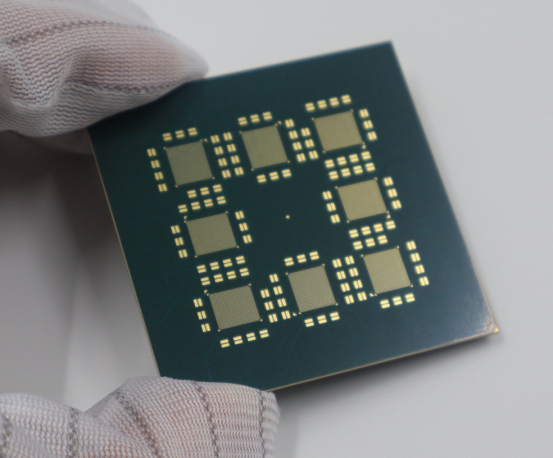
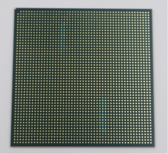
A printed circuit board (PCB) is a flat board that mechanically supports and electrically connects electronic components using conductive pathways, also called traces. These traces are usually made of copper and are carefully arranged to create specific electrical circuits. The main components of a PCB include the substrate, which is the insulating base; the conductive pathways that carry electrical signals; and the electronic components such as resistors, capacitors, and integrated circuits that perform specific functions.
PCBs are the backbone of almost every modern electronic device. They replace bulky and fragile point-to-point wiring, allowing circuits to be compact, reliable, and easier to manufacture. For example, a smartphone contains dozens of PCBs, each connecting hundreds of components in an organized and efficient layout. Without PCBs, modern electronics would be larger, more expensive, and far less reliable.
Significance in Electronics Evolution
The invention of PCBs marked a turning point in electronics. Before PCBs, devices relied on hand-wired connections, which were prone to errors and difficult to scale. Early electronic assemblies often required meticulous manual soldering, which limited production speed and increased costs.
By providing a standardized platform for component placement and electrical connectivity, PCBs enabled miniaturization, allowing devices to become smaller, lighter, and more powerful. They also facilitated mass production, because the same PCB design could be replicated thousands of times with consistent quality. For instance, radios and early televisions became more affordable and reliable thanks to the adoption of PCBs, compared with their hand-wired predecessors.
Overview of the First PCB
The first printed circuit board was developed in the early 1940s, during a period of rapid technological advancement. Austrian engineer Paul Eisler is widely credited with creating the first practical PCB in 1943 while working on a radio project in England. This early PCB used a single-layer copper pattern on an insulating substrate to replace complex wire connections, demonstrating a compact and more reliable approach to circuit assembly.
The introduction of this first PCB laid the foundation for the electronics industry we know today. Its design principles—substrate, copper traces, and component mounting—remain at the core of all modern PCBs, from simple consumer gadgets to advanced aerospace systems. By replacing tangled wires with organized, replicable circuits, the first PCB not only solved technical problems but also opened the door for rapid innovation across electronics.
Origins of the First Printed Circuit Board
Early Concepts and Prototypes
The idea of creating a flat board to organize and connect electronic components existed long before modern PCBs. Early experiments often involved point-to-point wiring on insulating boards, where wires were manually soldered between components. Engineers sometimes used wiring boards, which were flat boards that held components in place and provided a rough layout for circuits.
Step by step, these early prototypes evolved:
1. Components were mounted on a rigid board for stability.
2. Conductive paths were drawn or glued onto the board to create connections.
3. Components were soldered to these paths to complete the circuit.
The materials used were crucial to their success. Early boards often relied on Bakelite or phenolic resin as insulating substrates, while copper foils formed the conductive traces. These materials provided durability, electrical insulation, and the ability to handle soldering temperatures, paving the way for the first practical printed circuit boards.
Key Inventors and Pioneers
The development of the first PCB involved several innovators. Paul Eisler, an Austrian engineer, is widely credited with creating the first functional PCB in 1943 while working on a radio project in England. Eisler’s approach replaced complex wiring with a single-layer copper pattern on an insulating board, dramatically simplifying assembly.
Other engineers experimented with similar ideas around the same time, though often in different contexts such as industrial equipment. Some focused on layered boards, aiming for higher component density, while others refined etching techniques to improve circuit precision. Comparing these approaches:
Eisler prioritized practical assembly and reliability for consumer devices.
Aerospace engineers experimented with multi-layer and high-frequency designs for advanced applications.
Together, these pioneers established the principles of substrate-based circuit design, trace routing, and component mounting that define PCBs today.
Challenges in Early PCB Development
Despite the promise of PCBs, early development faced significant hurdles. Manufacturing was largely manual, with no automated etching or soldering processes, limiting scalability. Producing consistent quality across multiple boards was difficult, and defects often caused circuit failures.
Technical challenges included:
Ensuring reliable electrical connections across the copper traces.
Preventing short circuits due to imperfect etching or material inconsistencies.
Balancing mechanical strength and electrical performance, especially in thin boards.
These limitations slowed widespread adoption initially but also drove innovation in materials, fabrication techniques, and design standards. Overcoming these early obstacles laid the groundwork for modern high-speed, multi-layer PCBs used in everything from smartphones to aerospace systems.
Design and Manufacturing of the First PCB
PCB Structure and Layers
Early printed circuit boards were mostly single-layer designs, meaning all the conductive pathways were placed on one side of the insulating substrate. Single-layer boards were simpler to produce and sufficient for basic electronics. Some experimental designs explored multi-layer boards, stacking several layers of substrates and copper traces to increase circuit density, but these were difficult to manufacture reliably at the time.
Material selection was a critical part of early PCB design. Bakelite and phenolic resin served as durable, heat-resistant substrates, while copper foils formed the conductive pathways. Engineers carefully planned the routing of these pathways to minimize interference and ensure consistent electrical performance. The combination of substrate and copper traces established the foundation for all PCB structures that followed.
Step-by-Step Fabrication Process
The fabrication of the first PCB followed several key steps:
1. Substrate Preparation: A flat insulating board was cut to size and cleaned to remove dust and oils.
2. Copper Application: A thin layer of copper foil was bonded to the substrate.
3. Circuit Patterning: The desired circuit layout was applied using masks or resist ink, leaving only the necessary copper paths exposed.
4. Etching: Chemical etchants removed the unwanted copper, leaving the precise conductive pathways intact.
5. Component Placement and Soldering: Components such as resistors, capacitors, and vacuum tubes were manually placed and soldered onto the board.
An early example of this process can be seen in radios produced in the 1940s. Aerospace equipment equipment also benefited from these methods, where early PCBs allowed for compact, reliable circuits in avionics and communications devices. These applications demonstrated the practical advantages of PCBs over traditional point-to-point wiring.
Comparison with Modern PCB Techniques
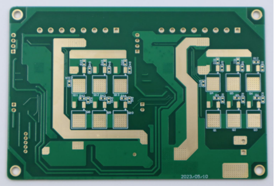
Modern PCB production has evolved dramatically compared with the first boards. Today’s PCBs use FR-4 fiberglass substrates, multi-layer designs, and high-precision etching, enabling high-density circuits and faster signal transmission. Automated assembly lines and surface-mount technology (SMT) allow thousands of components to be placed with accuracy far beyond what was possible in the 1940s.
The evolution from manual to automated fabrication illustrates the growth of electronics manufacturing. While early PCBs relied on simple materials and labor-intensive processes, modern techniques focus on miniaturization, high-frequency performance, and mass production scalability. This transformation has enabled the development of compact smartphones, advanced medical devices, and aerospace electronics that would have been impossible with the first-generation PCB methods.
Impact on Technology and Industry
Influence on Consumer Electronics
The introduction of printed circuit boards transformed consumer electronics by enabling smaller, more reliable, and mass-producible devices. Early applications included radios, televisions, and calculators, where PCBs replaced complex hand-wired connections. This allowed manufacturers to reduce production errors, lower costs, and deliver products to a growing market more efficiently.
For example, radios in the 1940s that used the first PCBs were more compact and easier to assemble than traditional wired versions. Televisions shortly after also began incorporating PCBs, which helped standardize component layouts and improve performance. Calculators in the 1960s further demonstrated how PCBs enabled miniaturization, allowing portable electronic devices to become widely accessible.
Aerospace Applications
Early PCBs had a significant impact on aerospace technology. They were used in radar systems, communication devices, and other critical electronics. By replacing bulky wiring with compact circuit boards, aerospace equipment became more reliable and easier to maintain under harsh conditions.
For example, avionics systems in aircraft and radar installations relied on PCBs for precise signal routing and reduced assembly time. Afterward, the adoption of PCB technology expanded into commercial and industrial aerospace, where multi-layer boards improved circuit density and enabled more sophisticated systems. These innovations laid the foundation for the complex electronics in today’s satellites and aircraft.
Industrial and Economic Implications
PCBs also drove major industrial and economic changes. By providing a reproducible and standardized platform, they enabled mass production of electronic devices, reducing labor costs and minimizing assembly errors. This standardization contributed to lower product prices and faster innovation cycles.
Compared to previous point-to-point wiring, PCBs offered clear advantages:
Reduced assembly time and human error.
Improved circuit reliability and durability.
Enabled higher component density and smaller devices.
As a result, electronics manufacturing became more scalable, efficient, and globally competitive. The shift from manual wiring to PCB-based production not only accelerated technological progress but also shaped the modern electronics industry, influencing everything from consumer gadgets to industrial machinery.
Evolution from First PCB to Modern Innovations
Material Advancements
Since the first PCBs made with Bakelite and phenolic resin, materials for circuit boards have evolved significantly. The introduction of FR-4, a fiberglass-reinforced epoxy laminate, provided superior mechanical strength, electrical insulation, and thermal stability. Modern flexible PCBs, made from polyimide or similar materials, allow circuits to bend or fold, enabling innovative designs in compact devices such as smartphones, wearables, and foldable electronics.
The benefits of these modern materials include:
Thermal stability: Can withstand higher soldering temperatures and operational heat.
Miniaturization: Allows denser component placement, supporting smaller, more powerful devices.
Durability: Reduces the risk of cracking or electrical failure under stress.
These advancements have dramatically expanded the applications of PCBs across multiple industries.
Technological Innovations
Beyond materials, PCB technology has advanced through innovations in design and manufacturing. Multi-layer boards enable more complex circuits by stacking multiple conductive layers separated by insulating substrates. Surface-mount technology (SMT) allows components to be mounted directly on the board’s surface, improving reliability and reducing size. High-Density Interconnect (HDI) boards use microvias and finer traces to further increase circuit complexity and signal performance.
Examples of these innovations include:
High-speed PCBs in computers and telecommunications equipment, which handle fast signal transmission with minimal interference.
Complex designs in aerospace or medical devices, where space constraints and reliability requirements demand advanced multi-layer and HDI solutions.
These technological advancements build on the original PCB concepts, enabling designs that were unimaginable with the first single-layer boards.
Future Trends
The next generation of PCB innovations focuses on flexibility, intelligence, and integration with emerging technologies. Flexible PCBs continue to expand into wearable electronics, while 3D PCBs allow vertical stacking of circuits for even higher density. Bio-integrated PCBs are being explored for medical implants, sensors, and electronics that interface directly with the human body.
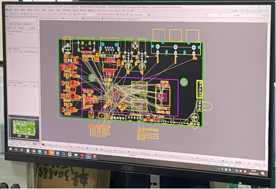
Additionally, AI-assisted PCB design is transforming how engineers create circuits. Automated layout optimization, predictive signal integrity analysis, and rapid prototyping are reducing design errors and accelerating production. Automated fabrication complements these tools, allowing complex boards to be manufactured efficiently at scale.
These trends indicate that PCBs will remain central to electronics innovation, continuing to evolve from the first copper-and-Bakelite boards to intelligent, high-performance, and integrated systems of the future.
Conclusion
The journey of the printed circuit board shows how a simple idea can revolutionize an entire industry. From early copper traces on Bakelite to today’s high-speed, multi-layer designs, the lessons of material choice, precision, and iterative design remain vital for engineers. Companies like PCBMASTER continue this legacy, turning innovation into reliable, high-performance PCB solutions for a rapidly evolving electronics world.
FAQs
What materials were used in the first printed circuit board?
The first printed circuit boards were made using Bakelite or phenolic resin as insulating substrates and copper foils for conductive pathways. Bakelite and phenolic resin provided durability and electrical insulation, while copper allowed for reliable electrical connections between components. These materials formed the foundation for early PCB designs and enabled compact, organized circuits.
Who is credited with inventing the first PCB and why?
Paul Eisler, an Austrian engineer, is widely credited with inventing the first practical printed circuit board in 1943 while working on a radio project in England. Eisler’s design replaced complex point-to-point wiring with a copper pattern on an insulating board, simplifying assembly, improving reliability, and demonstrating the potential of PCB technology for mass production.
How did the first PCB improve electronics compared to traditional wiring?
The first PCB improved electronics by replacing messy, error-prone hand-wired connections with organized copper traces on a flat board. This allowed devices to be smaller, more reliable, and easier to assemble, while reducing production time and minimizing wiring errors. Radios, televisions, and early calculators became more compact and affordable thanks to this innovation.
What were the biggest challenges in manufacturing early PCBs?
Early PCB manufacturing faced several challenges, including manual fabrication processes, inconsistent quality, and difficulty in scaling production. Engineers had to ensure reliable electrical connections and prevent short circuits, while working with materials and etching techniques that were less precise than today’s standards. These limitations initially slowed adoption but also drove innovation in materials and fabrication methods.
How has PCB technology evolved from the first boards to today’s high-speed designs?
PCB technology has evolved from single-layer Bakelite boards to multi-layer, high-density, and flexible PCBs. Modern boards use materials like FR-4 fiberglass for strength and thermal stability, and employ surface-mount technology (SMT), high-density interconnect (HDI) designs, and automated fabrication. These advancements enable high-speed signal transmission, miniaturization, and complex circuit designs in everything from smartphones to aerospace systems.

