


Modern PCB Technology: Ensuring High-Quality Manufacturing
Modern PCB technology is essential for ensuring high-quality manufacturing, meeting the rigorous standards required by industries like electronics, automotive, and healthcare. Thanks to advancements in materials and production methods, modern PCBs are now smaller, faster, and more reliable, which is critical for devices in these fields where precision and durability matter most.
In industries like automotive, where safety is a top priority, high-quality PCBs must perform reliably under harsh conditions and over long periods. Similarly, in healthcare, precise and stable PCBs are vital for ensuring medical equipment functions accurately, providing life-saving data with minimal risk.
Innovations such as high-density interconnects (HDI), automation, and advanced testing systems have made it possible to meet these demanding requirements. These technologies enable manufacturers to produce PCBs that not only perform well but also last longer, reduce costs, and enhance the overall performance of devices. As these technologies evolve, they continue to drive improvements in quality and safety across a wide range of industries.
Key Foundations of High-Quality PCBs: Advanced Technologies and Precision Materials
High-Frequency and High-Density Interconnect (HDI) Technology
High-frequency laminates and metal core substrates are critical materials used in modern PCB manufacturing. High-frequency laminates improve signal integrity by reducing signal loss, making them ideal for communication devices like smartphones and 5G equipment. Metal core substrates help manage heat better, which is especially important for devices that generate a lot of heat, such as automotive electronics or LED lighting. These materials ensure that the PCB operates efficiently and remains stable under varying temperatures.
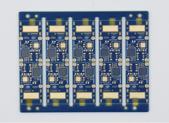
HDI technology allows for smaller, more complex designs in PCBs by using advanced techniques like microvias and stacked vias. It enables the creation of multilayer PCBs that can handle more connections in a smaller area. This is essential in industries requiring compact, high-performance devices, such as wearables, medical devices, and consumer electronics. The increased design density allows manufacturers to pack more components into the same board space, increasing performance without expanding the device size.
Precision Manufacturing Technologies
Advanced precision manufacturing techniques are key to achieving high-quality PCBs. Laser drilling and microvia technology are commonly used for creating small, precise holes in PCBs. Laser drilling uses a focused laser beam to drill micro-holes with extreme accuracy, which is ideal for creating microvias—tiny holes that connect different layers of a PCB. These holes are often used in HDI designs and allow for more compact and complex circuit layouts.
In addition to laser drilling, high-precision photolithography is essential in PCB manufacturing. This technique involves projecting light through a mask onto a photosensitive material, creating intricate patterns on the PCB. The accuracy of photolithography directly impacts the precision of PCB traces, which are the electrical pathways that connect components. High-resolution photolithography ensures that traces are extremely fine, enabling the production of PCBs with higher performance and greater reliability. This is especially important for high-speed applications like networking equipment and high-frequency devices, where even the smallest imperfections in the traces can lead to signal degradation or device failure.
These manufacturing advancements ensure that modern PCBs can meet the growing demands of industries that require high-performance, compact, and reliable electronic devices. By combining precision materials and state-of-the-art manufacturing processes, manufacturers can produce PCBs that not only meet functional requirements but also offer long-term durability and performance.
Automation and Smart Technologies: Improving Production Efficiency and Quality Consistency
Automated Production Processes
High-speed pick-and-place machines and automated reflow soldering are critical in modern PCB assembly for ensuring high accuracy and quality. The pick-and-place machine is designed to place tiny components on a PCB with incredible precision, often at speeds exceeding 50,000 components per hour. This allows for rapid assembly without compromising accuracy. These machines use advanced vision systems to identify and correctly place components, ensuring they align perfectly on the board. In high-volume manufacturing, this level of precision significantly reduces human error and the potential for faulty connections.
Automated reflow soldering is another essential part of the process. It involves passing the assembled PCB through a reflow oven, where heat melts solder paste, forming strong, reliable connections between components and the PCB. The oven is programmed to maintain exact temperatures, typically within a range of ±0.5°C, which ensures that all solder joints are uniform and reliable. This automation minimizes the risk of defects like cold solder joints, which can cause intermittent failures in electronic devices.
In addition to improving quality, automation reduces labor costs and shortens production cycles. By automating these processes, manufacturers can produce PCBs faster and more efficiently, meeting tight deadlines and reducing operational costs. This is especially important in industries where high-volume production and cost-effective manufacturing are key, such as consumer electronics and automotive sectors.
Applications of Artificial Intelligence and Machine Learning
AI-powered defect detection and process optimization are transforming PCB manufacturing. Artificial intelligence systems are capable of inspecting every PCB with high accuracy, identifying defects such as misplaced components, incorrect solder joints, or damaged traces. AI-based Automated Optical Inspection (AOI) systems scan the boards in real-time and compare them to pre-set standards, detecting even the smallest anomalies that may go unnoticed by human inspectors. This technology not only speeds up the inspection process but also increases defect detection accuracy, significantly improving the overall product quality.
Machine learning (ML) further enhances PCB manufacturing by optimizing production processes. By continuously analyzing data from previous production cycles, ML algorithms can predict potential issues and suggest adjustments to improve efficiency. For example, if a certain design consistently leads to soldering defects, machine learning can adjust parameters in real-time, such as temperature profiles or component placement techniques, to reduce those defects in future production runs.
Machine learning also allows manufacturers to adapt to different design requirements with minimal manual intervention. In PCB production, designs can vary greatly in terms of complexity and size. ML systems can automatically adjust settings, like component placement speed or soldering temperatures, based on the specific characteristics of the design. This level of flexibility is invaluable, especially when switching between different types of PCBs, such as those used in consumer electronics versus those for high-frequency applications like 5G devices.
In summary, automation and AI-driven technologies improve both the speed and consistency of PCB production. Automation reduces human error and labor costs, while AI and machine learning bring greater precision and adaptability to the manufacturing process, ensuring high-quality, reliable PCBs. These advancements not only make production more efficient but also ensure that every board meets strict quality standards, benefiting industries that rely on high-performance, reliable electronics.
Strict Inspection Systems: Multi-Layer Protection for PCB Quality
Automated Optical Inspection (AOI)
AOI systems are crucial in modern PCB manufacturing for detecting surface defects with precision and speed. These systems use high-resolution cameras and advanced software to scan the PCB surface, identifying issues like misaligned components, incorrect solder joints, and broken traces. AOI systems can inspect every board quickly, ensuring that each one meets the required quality standards. Compared to manual inspection, AOI significantly increases inspection efficiency and quality control, reducing the chances of human error.
When combined with AI technology, AOI systems can further enhance detection accuracy. AI-powered AOI can analyze images in real-time, recognizing patterns and anomalies that may not be easily detectable with traditional methods. For example, AI can differentiate between normal component variations and actual defects, improving the system's ability to identify subtle issues that might otherwise be overlooked. This AI-driven precision not only boosts the quality of the final product but also ensures that defects are caught early in the production process, minimizing waste and rework.
X-Ray Inspection Technology
X-ray inspection plays a vital role in detecting hidden defects, especially in multilayer PCBs. Traditional inspection methods, like visual checks, may not catch internal issues that occur within the layers of a PCB, such as BGA (Ball Grid Array) soldering defects. X-ray systems can see through the layers of the PCB and reveal problems like poor solder connections, voids (gaps in the solder), or misalignment of internal components. This technology is essential for ensuring the performance and reliability of complex, high-density PCBs used in smartphones, medical devices, and automotive electronics.
By using X-ray inspection, manufacturers can assess the quality of internal connections and make adjustments as needed. This level of inspection guarantees that the PCB will function properly even in the most demanding conditions. The ability to detect these hidden flaws early helps ensure that long-term reliability is maintained, preventing costly failures or repairs after the PCB is deployed in end-use applications.
Functional Testing and Flying Probe Testing
Functional testing is designed to evaluate whether the PCB performs as expected in real-world conditions. This testing method simulates actual usage by applying power and checking for correct electrical behavior, such as signal integrity, voltage levels, and current flow. Functional testing is crucial for ensuring that every component on the board works as it should before the PCB is sent out for use in end products like smartphones, cars, or medical devices. This testing verifies that the board's electrical functions align with the design specifications, ensuring reliability and performance under typical operational conditions.
On the other hand, flying probe testing is a more flexible method used in small-batch production or prototype testing. Unlike traditional in-circuit testing, which uses a fixed fixture, flying probe testing uses movable probes to check individual points on the PCB. This method is ideal for designs that are still in development or for small production runs, as it allows for fast setup and fewer limitations. Flying probe systems are particularly useful for detecting short circuits, open circuits, and incorrect component placements, ensuring the PCB’s functionality before it goes into mass production.
Both functional testing and flying probe testing play important roles in ensuring that a PCB operates correctly and reliably, catching any flaws that might affect its performance in the field. They help manufacturers deliver high-quality PCBs that meet the functional and safety requirements of their respective industries.
Continuous Improvement and Optimization in PCB Manufacturing
Six Sigma and Data-Driven Optimization Methods
Six Sigma is a powerful methodology used to improve PCB manufacturing processes by identifying and eliminating defects. The goal of Six Sigma is to reduce variation and improve the consistency of the production process. By analyzing production data, manufacturers can pinpoint areas where defects are likely to occur, such as misalignment in component placement or issues in soldering. Once these areas are identified, corrective actions can be taken to standardize the process, leading to fewer errors and higher-quality PCBs.
Six Sigma uses a structured approach known as DMAIC (Define, Measure, Analyze, Improve, Control) to improve processes. In PCB manufacturing, this means carefully defining quality standards, measuring performance, analyzing data for defects, making improvements, and then controlling the process to ensure the changes are sustainable. For example, a manufacturer might find that the error rate for component placement is higher than expected, and by using Six Sigma methods, they can reduce that error rate by improving machine calibration or changing the placement speed.
Data-driven monitoring systems are another essential tool for real-time quality control in PCB production. These systems collect and analyze data from various stages of the manufacturing process, such as component placement, soldering, and testing. By continuously monitoring these data points, manufacturers can detect issues as they arise, allowing them to adjust the process immediately. For example, if a temperature fluctuation is detected in the reflow soldering process, the system can trigger an automatic adjustment to prevent poor solder joints. This real-time feedback not only reduces defects but also supports continuous improvement, ensuring that each batch of PCBs meets the desired quality standards.
Feedback Mechanisms and Iterative Optimization
A feedback mechanism is critical in ensuring that each PCB batch meets the required quality standards. In PCB manufacturing, this feedback comes from inspection results, testing data, and performance reviews. Once a defect or issue is identified, it’s important to feed this information back into the process to make necessary adjustments. This feedback loop allows for continuous monitoring of production, and ensures that even small quality issues are addressed before they impact larger batches of PCBs.
For example, if a batch of PCBs fails the automated optical inspection (AOI) system, the issue is flagged and the production team can investigate the cause. The feedback mechanism helps quickly identify whether the problem lies in the soldering process, component placement, or material quality. Adjustments can then be made in real time, preventing the same issue from occurring in future production runs.
Iterative optimization involves using data from tests and inspections to gradually improve the design and manufacturing process. As feedback is gathered, the production team analyzes the root causes of defects or inefficiencies and uses that information to make improvements. Over time, this iterative process leads to higher quality, more reliable PCBs. For example, if testing data indicates that a specific PCB design causes frequent failure during functional testing, adjustments can be made to the design, such as changing component placement or material selection, to improve the overall performance.
Through continuous feedback and optimization, manufacturers can steadily improve the quality of their products, reducing defects and enhancing production efficiency. This process of iterative optimization not only benefits manufacturers by improving the quality and reliability of their products but also helps meet the evolving demands of the market and ensure customer satisfaction.
Compliance with International Standards and Regulations: Ensuring Quality Assurance
ISO and IPC Standards
ISO 9001 and IPC Class 3 standards are essential for ensuring the reliability and quality of PCBs in various industries. These internationally recognized standards provide clear guidelines for manufacturing processes, helping to ensure that PCBs are produced to meet strict performance and safety criteria.
ISO 9001 is a quality management standard that focuses on ensuring consistent product quality and continuous improvement. For PCB manufacturers, adhering to ISO 9001 ensures that production processes are well-documented, controlled, and optimized for high efficiency. This standard emphasizes risk management, quality control, and customer satisfaction, ensuring that the final product consistently meets customer specifications. For example, a manufacturer producing medical or aerospace PCBs would follow ISO 9001 to guarantee that their products are both reliable and safe under the most demanding conditions.
IPC Class 3 is a standard specifically for high-reliability PCBs, particularly in industries where failure is not an option, such as aerospace, automotive, and medical devices. Class 3 ensures that the PCB can handle severe environmental conditions, such as extreme temperatures and vibrations, and function for a long time without failure. To meet IPC Class 3 standards, manufacturers must ensure the highest quality of components, precise assembly, and rigorous testing to confirm that the PCB can perform under demanding conditions. For example, PCBs used in automotive safety systems must meet IPC Class 3 to ensure they continue to operate flawlessly throughout the vehicle’s lifetime.
By following ISO 9001 and IPC Class 3 standards, PCB manufacturers can demonstrate their commitment to producing reliable, safe, and high-quality products that meet industry expectations.
Environmental Compliance and Regulations
Environmental regulations, such as RoHS and WEEE, play a significant role in shaping PCB manufacturing processes and materials. These regulations are designed to reduce the environmental impact of electronic waste and improve sustainability in the manufacturing process.
RoHS (Restriction of Hazardous Substances) is a regulation that limits the use of certain hazardous materials in electronic products. For PCB manufacturers, this means eliminating substances like lead, mercury, cadmium, and certain flame retardants from their production. By complying with RoHS, manufacturers ensure that their products are safer for both the environment and human health. For example, PCBs used in consumer electronics, such as smartphones and computers, must meet RoHS standards to ensure that harmful substances are not present in the final product.
WEEE (Waste Electrical and Electronic Equipment) is another important regulation that addresses the disposal of electronic waste. WEEE requires manufacturers to take responsibility for the collection and recycling of their products at the end of their life cycle. For PCB manufacturers, this means designing products that are easier to recycle and ensuring that they comply with disposal standards. This regulation encourages manufacturers to use recyclable materials and reduces the environmental impact of e-waste.
Together, RoHS and WEEE regulations influence material selection and production processes in PCB manufacturing. For example, manufacturers may opt for lead-free solder or eco-friendly laminates that comply with RoHS, and they may design PCBs that can be easily recycled to meet WEEE standards. These environmental regulations ensure that PCB manufacturers contribute to reducing the ecological footprint of electronic devices.
Conclusion
As technology continues to evolve, modern PCB manufacturing will keep pushing the boundaries of quality, enabling electronic products to achieve higher performance, smaller sizes, and lower power consumption. Advances in materials, precision manufacturing, and testing methods will enhance the reliability and functionality of PCBs, making them critical components in the next generation of electronics.
The future of PCB production will also see further integration of AI, automation, and smart manufacturing. These technologies will optimize production processes, allowing for faster, more accurate quality control and minimizing defects. As a result, manufacturers can expect to produce PCBs with greater efficiency and consistency, meeting the growing demands for complex, high-performance electronics in industries like automotive, telecommunications, and healthcare.
At PCBMASTER, we continuously apply cutting-edge PCB manufacturing technologies to support the development of high-quality products across various sectors. Our commitment to innovation ensures that we are ready to meet the challenges of tomorrow's electronic needs, driving the high-quality development of the manufacturing industry.
FAQs
Why is Automated Production Crucial for PCB Quality?
Automated production significantly boosts efficiency, reduces human error, and ensures high precision in component placement and consistent soldering quality. By relying on machines and robotics for tasks like component placement and soldering, the process is more accurate and faster compared to manual methods. Automation also helps maintain consistency across large volumes of production, ensuring each PCB meets the same high standards.
What Role Does X-Ray Inspection Play in Multi-Layer PCBs?
X-ray inspection is vital for detecting internal defects in multi-layer PCBs that cannot be easily identified through traditional optical methods. This technology allows manufacturers to see through the layers of the PCB, ensuring the quality of internal connections, such as Ball Grid Arrays (BGAs), and verifying the integrity of solder joints and vias. By uncovering hidden flaws, X-ray inspection ensures the reliability and long-term performance of multi-layer PCBs, which are critical in complex applications like automotive electronics and medical devices.
How Can AI Enhance Quality Control in PCB Manufacturing?
AI systems can significantly improve quality control in PCB manufacturing by continuously monitoring the production process in real time. These systems can automatically adjust parameters such as temperature or pressure during soldering, ensuring optimal conditions for each batch. Additionally, AI-powered defect detection systems can spot issues like misaligned components or faulty solder joints with high accuracy, allowing manufacturers to address problems immediately. By integrating AI into the manufacturing process, companies can achieve higher production efficiency, reduced waste, and more consistent product quality.
Author Bio
Hi, I'm Carol, the Overseas Marketing Manager at PCBMASTER, where I focus on expanding international markets and researching PCB and PCBA solutions. Since 2020, I've been deeply involved in helping our company collaborate with global clients, addressing their technical and production needs in the PCB and PCBA sectors. Over these years, I've gained extensive experience and developed a deeper understanding of industry trends, challenges, and technological innovations.
Outside of work, I'm passionate about writing and enjoy sharing industry insights, market developments, and practical tips through my blog. I hope my posts can help you better understand the PCB and PCBA industries and maybe even offer some valuable takeaways. Of course, if you have any thoughts or questions, feel free to leave a comment below—I'd love to hear from you and discuss further!

