


Why Minimalist Circuit Board Prints Are the Future of PCB Design
The heart of every electronic device lies in its circuit board, but what if this core structure could be drastically simplified, offering the same (or even better) performance? This is where minimalist circuit board prints come in—designs that prioritize clean, efficient layouts over cluttered complexity. Instead of layering components and connections, minimalist designs focus on essentials, reducing both size and cost without sacrificing functionality. As the demand for smaller, more powerful devices grows, this design philosophy is becoming the new standard, pushing the boundaries of innovation in ways traditional PCB designs never could.
Introduction to Minimalist Circuit Board Prints
Definition and Concept of Minimalist PCB Design
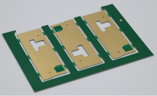
Minimalist circuit board prints represent a departure from traditional PCB designs by focusing on simplicity and efficiency. At their core, minimalist PCBs aim to reduce complexity—using fewer components, simpler traces, and cleaner layouts without sacrificing functionality. This approach embraces the idea that less is more, making it possible to create more compact and cost-effective designs without compromising on performance.
Key Characteristics of Minimalist PCBs:
Reduced Components: Minimalist designs prioritize the essential components required for a device’s functionality, eliminating unnecessary elements. By using multifunctional components or integrating features into fewer parts, the overall component count is reduced.
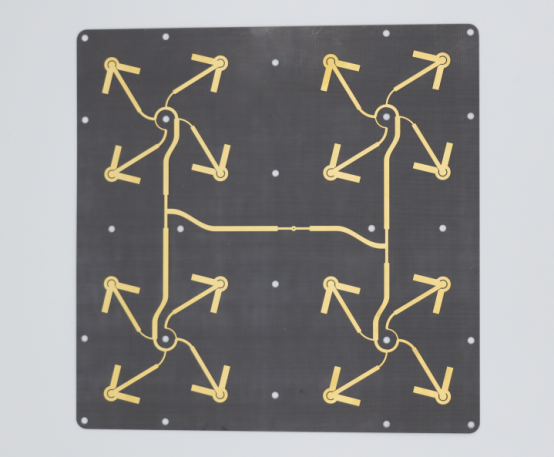
Simpler Traces: Trace routing in minimalist PCBs is streamlined, cutting down on unnecessary intersections and detours. This minimizes the risk of signal interference and improves performance.
Clean Layouts: The overall layout is designed with clarity in mind, often resulting in simpler, more organized board structures. This clean design leads to more efficient manufacturing and assembly.
Comparison with Traditional PCBs:
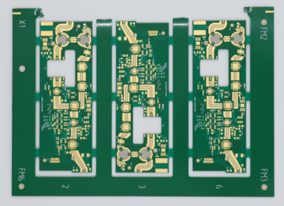
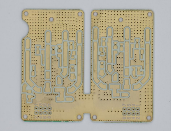
Traditional PCBs typically prioritize robustness, with multiple layers, many components, and intricate trace designs. While these boards are well-suited for complex systems, they tend to be bulkier, costlier, and less efficient in terms of space and power consumption. In contrast, minimalist PCBs strip away excess, making the design more focused, efficient, and scalable, especially for compact devices like wearables, IoT gadgets, and smartphones.
Importance of PCB Design Evolution
The evolution of PCB design has been driven by the constant need for efficiency, cost reduction, and miniaturization. Over the past few decades, as technology has advanced, the role of PCBs in electronic devices has become increasingly crucial. Early PCB designs were large, often multi-layered, and packed with components that provided functionality at the expense of size and cost.
A Brief History of PCB Design Trends:
1970s-1980s: The first generations of PCBs were quite simple, typically single-layered designs with few components. These boards were often large and bulky.
1990s-2000s: Multi-layered PCBs began to dominate, allowing for more complex electronics. The focus shifted towards improving performance and integrating more features into smaller packages.
2010s-Present: As the demand for smaller, more efficient devices grew (smartphones, wearables, IoT), designers started to prioritize compactness and simplicity in PCB design, laying the groundwork for minimalist approaches.
The Shift Toward Minimalism:
The current trend in PCB design is rooted in the drive for miniaturization—making devices smaller, lighter, and more powerful. With advances in materials and fabrication techniques, designers can now create simpler, smaller boards that achieve the same or better performance than their larger, more complex counterparts.
Minimalist PCBs are now seen as a key enabler of this shift. These designs focus on optimizing the available space, reducing the number of components, and simplifying the overall layout—all while maintaining functionality and reliability. As more devices enter the market that require smaller form factors, minimalist PCBs are expected to become even more prevalent in the coming years.
This shift is especially evident in industries like wearables, where every square millimeter counts, and IoT, where devices need to be as small and efficient as possible. The trend toward minimalist design allows for faster production cycles, reduced costs, and more reliable devices, making it a practical choice for both high-volume and cutting-edge electronics.
Benefits of Minimalist Circuit Board Prints
Cost Efficiency
One of the primary benefits of minimalist circuit board prints is their ability to significantly reduce production costs. By simplifying the design and cutting out unnecessary components, manufacturers can lower both material and labor expenses.
Fewer Components = Lower Production Costs: Minimalist PCBs use only the essential components needed for the device's functionality, reducing the overall bill of materials. With fewer parts to source and assemble, the total manufacturing cost decreases.
Reduced Material Usage and Simplified Assembly: The streamlined design not only reduces the need for extra components but also leads to savings in raw materials. Fewer layers, fewer traces, and fewer soldering points result in less time spent on assembly and fewer resources used during production.
Example:
In a comparison between a traditional PCB for a smartphone and a minimalist PCB, the latter could eliminate redundant parts such as multiple capacitors, resistors, or separate components for power management. As a result, the minimalist PCB would cost significantly less to produce, with estimates showing savings of up to 30% in some cases. This can have a profound impact on the final cost of consumer electronics, making it more affordable for manufacturers and consumers alike.
Enhanced Reliability and Performance
Minimalist circuit boards tend to offer improved reliability and better performance due to their simpler design and fewer components.
Fewer Points of Failure: The fewer the components and connections, the fewer the potential points of failure. Minimalist designs minimize the risk of issues like faulty connections or component breakdowns that might occur with more complex boards.
Easier Signal Routing and Reduced Interference: With less complexity in the layout, it becomes easier to route signals through the board. Fewer traces and more direct routing paths reduce the likelihood of signal interference and noise, leading to better performance, especially in high-frequency applications.
Step-by-Step Example:
Imagine simplifying a multi-layer PCB used in a wearable fitness tracker. In a traditional design, numerous layers and components are required for functions like power management, sensors, and communication modules. By converting this to a minimalist PCB, a designer could consolidate functions into a single layer or fewer components, reducing both the trace length and the number of connections. This streamlined layout would decrease the chance of signal degradation or electrical noise, resulting in a more reliable and higher-performing product.
Space and Weight Reduction
Another significant advantage of minimalist circuit board prints is their ability to save both space and weight—key factors for portable and wearable devices.
Compact Design for Portable Devices: The reduced number of components and simplified layout allow for smaller, thinner boards. This is especially valuable in industries where space constraints are a primary concern, such as in smartphones, wearables, and IoT devices.
Weight Reduction for Wearables and Drones: For devices like fitness trackers, smartwatches, and drones, every gram counts. Minimalist PCBs reduce the overall weight of the device, contributing to better user comfort, longer battery life, and increased portability.
Comparison:
A comparison between the PCB in a smartphone and a minimalist PCB reveals that the latter is significantly smaller and lighter. For example, minimalist PCBs in wearables like smartwatches can be up to 50% smaller than their traditional counterparts, making them more suitable for designs where compactness and weight are critical factors. This enables manufacturers to create devices that are not only high-performing but also sleek and portable.
Faster Production and Prototyping
The simplicity of minimalist PCB designs also leads to faster production and prototyping.
Simplified Design Speeds Up Prototyping: Since minimalist PCBs use fewer components and layers, designers can develop and iterate prototypes faster. This reduction in complexity leads to quicker design cycles, enabling faster testing and time-to-market for new products.
Reduced Testing Time Due to Fewer Components: With fewer components and simpler layouts, there’s less to test. This can shorten the overall testing phase, allowing for faster validation of the final product before it enters full-scale production.
Example:
Consider a company developing a new smart home device. By using a minimalist PCB design, the team can create an initial prototype in a matter of weeks, compared to a traditional design that might take several months to develop, test, and iterate. The reduced number of components and simpler design ensures faster validation and fewer errors, accelerating the product's release to market.
These key benefits—cost efficiency, enhanced reliability, space and weight reduction, and faster production—make minimalist circuit board prints an ideal choice for a wide range of modern electronics, driving innovation and efficiency across industries.
Design Principles for Minimalist Circuit Boards
Component Optimization
One of the key principles in minimalist circuit board design is component optimization. This approach focuses on choosing fewer, but more versatile components to reduce complexity while maintaining performance.
Choosing Multifunctional ICs: In minimalist PCB design, instead of using multiple separate components for different functions (e.g., power regulation, signal processing), designers opt for multifunctional integrated circuits (ICs). These ICs combine several functionalities into a single component, thereby reducing the overall number of parts on the board. For example, an analog-to-digital converter (ADC) could be integrated into a microcontroller rather than using separate chips for each function.
Component Consolidation Techniques: Common strategies for component consolidation include using system-on-chip (SoC) solutions, where multiple functionalities are combined into a single chip, and integrated passive devices (IPDs), which combine resistors, capacitors, and inductors into one unit. These techniques not only reduce the number of components but also save space and improve reliability by minimizing the risk of connection failures.
Example:
In a smartphone design, instead of using multiple chips for Wi-Fi, Bluetooth, and GPS, designers can use a multifunctional RF IC that consolidates all these capabilities into one chip. This dramatically reduces the PCB size and complexity, contributing to a thinner and more efficient device.
Efficient Trace Routing
Efficient trace routing is a critical design principle for minimalist PCBs. By minimizing trace length and optimizing the path for signal flow, designers can create simpler, more efficient boards that perform better.
Strategies for Minimizing Trace Length: One of the most effective ways to simplify a PCB is by reducing the length of the traces. This can be achieved by strategically placing components to minimize the distance signals must travel. Using surface-mount devices (SMDs) instead of through-hole components can also help reduce trace length because SMDs require fewer routing paths.
Layer Reduction Techniques: Traditional PCBs often use multiple layers to manage routing and component placement. However, minimalist PCBs typically aim to reduce the number of layers, often opting for single-layer or dual-layer designs. By using high-density interconnect (HDI) technologies or compact routing methods, it’s possible to achieve the same functionality with fewer layers, reducing both manufacturing costs and board size.
Step-by-Step Example:
To convert a traditional multi-layer PCB into a minimalist, single-layer design, the following steps could be taken:
1. Identify essential components and consolidate multifunctional parts to reduce the number of components.
2. Rearrange the layout to ensure signal paths are as short as possible. For instance, the power and ground traces should be placed close to each other to reduce noise and interference.
3. Use vias sparingly or avoid them altogether. Minimize the use of vias by designing the layout in such a way that components are placed in a manner that allows for efficient routing on a single layer.
4. Test for electrical integrity after the layout is optimized, ensuring the shorter traces do not interfere with signal quality.
This approach results in a simpler, more cost-effective PCB, ideal for small form-factor devices like wearables or IoT gadgets.
Power and Thermal Management
In minimalist PCBs, power distribution and thermal management are crucial because the design's simplicity often means fewer ways to manage heat dissipation or power flow.
Techniques to Handle Power Distribution: Minimalist designs often require more efficient power management. Designers can use power planes and decoupling capacitors to ensure stable voltage levels throughout the board. Additionally, integrated voltage regulators can replace separate power management components, improving both the design’s simplicity and energy efficiency.
Thermal Management in Compact Layouts: Since minimalist PCBs typically have fewer layers and components, heat dissipation can become a challenge. Designers often incorporate heat sinks, thermal vias, or thermal pads into the design to help spread heat away from sensitive components. For example, a wearable fitness tracker may integrate small thermal vias that connect heat-generating components to the PCB's ground plane, improving thermal distribution.
Case Study:
Consider a smartwatch with a minimalist PCB. Due to the compact design, managing the heat generated by the processor is critical. By using a combination of thermal vias and heat-conducting materials within the PCB, the heat generated by the processor is efficiently transferred to the watch's case, preventing overheating and ensuring that the device remains comfortable to wear.
Aesthetic and Functional Balance
Minimalist circuit board design is not just about simplicity—it's about striking a balance between aesthetics and functionality. A well-designed minimalist PCB can improve both the performance and the visual appeal of the final product.
How Minimalism Improves Functionality: By removing unnecessary components and simplifying layouts, minimalist designs can improve the overall functionality of the PCB. Shorter trace lengths reduce signal interference, while fewer components can improve reliability. This makes the PCB more durable and less prone to failure, which is especially important for devices used in demanding environments.
Enhancing Visual Design: In consumer electronics, the visual appeal of the PCB is just as important as its functionality. Minimalist designs often result in sleek, compact, and visually appealing devices. For example, many modern smartphones use minimalist PCBs that are integrated seamlessly into the overall design, contributing to their slim, elegant appearance.
Examples from High-End Consumer Electronics:
Smartphones: The minimalist PCB in modern smartphones allows for a clean, streamlined design that fits perfectly into ultra-thin devices.
Wearables: Devices like smartwatches benefit from minimalist PCB designs that reduce both size and weight, enabling sleek, attractive aesthetics without sacrificing performance.
Minimalist PCBs are not just functional—they also support a high level of aesthetic integration, allowing them to be incorporated into beautifully designed products that are both user-friendly and visually appealing.
The design principles of minimalist PCBs—component optimization, efficient trace routing, power and thermal management, and the balance between aesthetics and functionality—are crucial to creating efficient, compact, and high-performance boards for modern electronics. These principles drive the evolution of technology, making it possible to produce smaller, lighter, and more reliable devices.
Applications Driving the Trend
Consumer Electronics
Minimalist circuit boards are playing a significant role in the evolution of consumer electronics. As devices become smaller, lighter, and more powerful, the need for efficient and compact PCBs has grown. This trend is especially evident in devices such as smartphones, tablets, and smartwatches.
Smaller PCBs in Smartphones, Tablets, and Smartwatches: Modern consumer electronics demand increasingly compact designs to fit within sleek, portable form factors. Minimalist PCBs help achieve these objectives by reducing the overall size of the board while maintaining full functionality. By using fewer components and optimizing layout, manufacturers can produce devices that are both powerful and ultra-compact.
Benefits in High-Volume Production: Minimalist PCBs offer significant cost savings in high-volume production. With simpler designs, fewer components, and shorter trace lengths, the manufacturing process becomes more efficient, reducing both production time and material costs. Additionally, these PCBs often require less testing, leading to faster time-to-market and lower costs per unit.
Example:
In smartphones, the use of minimalist PCBs allows for slimmer designs without compromising on features. The integration of multifunctional components and optimized routing techniques enables devices to remain thin, light, and packed with capabilities, such as advanced cameras, processors, and wireless connectivity.
Industrial and Medical Electronics
Minimalist PCBs are also making a significant impact in industrial and medical electronics, where size, efficiency, and reliability are critical. Devices in these sectors often need to operate in demanding environments, making compact, efficient PCB designs even more essential.
Compact PCB Designs in Medical Devices and Sensors: The trend toward minimalist PCBs is particularly useful for medical devices and sensors, where space and power consumption are crucial factors. These compact designs can be used in devices such as wearable health monitors, implantable sensors, and point-of-care diagnostics, enabling them to function effectively without bulky hardware.
Examples of Applications:
- Portable Monitoring Devices: Minimalist PCBs are ideal for portable ECG monitors or blood glucose meters, where size and ease of use are paramount. These devices require efficient layouts to pack advanced sensing capabilities into small, lightweight units.
- IoT Sensors: For IoT devices, minimalist PCB designs enable small, low-power sensors that can be easily integrated into a wide range of industrial applications. Examples include temperature and humidity sensors for smart agriculture, environmental monitoring, and industrial automation systems.
By leveraging minimalist PCBs, manufacturers can design smaller, more efficient medical devices that offer improved user experience and more precise monitoring, all while maintaining high performance in challenging environments.
Emerging Technologies
Minimalist circuit boards are increasingly being utilized in emerging technologies, where miniaturization and form factor flexibility are essential. Devices such as wearables, IoT devices, drones, and miniaturized robotics are driving the demand for compact, high-performance PCBs.
Wearables, IoT Devices, Drones, and Miniaturized Robotics: These technologies require extremely small and efficient circuit boards to function in constrained spaces while maintaining high performance. Minimalist PCBs allow for smaller, lighter devices that can still perform complex tasks, from health monitoring to real-time data transmission and autonomous navigation.
How Minimalist PCBs Enable Innovation in Form Factor: The use of minimalist PCBs enables manufacturers to design devices with unique form factors that were previously unthinkable. For instance, wearable devices like smartwatches and fitness trackers can be made significantly smaller without sacrificing battery life or functionality. Similarly, IoT sensors integrated into small devices can now be embedded in everyday objects, such as clothing, appliances, or infrastructure.
Example:
In drones, the use of minimalist PCBs allows for more compact designs, reducing weight and increasing flight time without compromising the drone’s capabilities. By using fewer components and optimizing the power distribution, designers can create more efficient drones that are both lightweight and high-performance, ideal for commercial and hobbyist applications alike.
Minimalist circuit boards are driving innovation across multiple industries, from consumer electronics to emerging technologies. Their ability to reduce size, improve efficiency, and maintain high performance is helping manufacturers meet the growing demand for compact, powerful devices. Whether it's for smartphones, medical devices, or the latest IoT gadgets, minimalist PCBs are shaping the future of electronics design.
Challenges and Solutions
Design Complexity
While minimalist PCB designs offer numerous benefits, they also come with the challenge of balancing simplicity with functionality. The goal of minimalist design is to reduce unnecessary elements while ensuring that the PCB can still support all the necessary functions of the device. Achieving this balance can be tricky, especially as modern devices require increasingly complex features in smaller form factors.
Balancing Minimalism with Functionality: The main challenge lies in ensuring that reducing the number of components or layers doesn’t compromise the performance of the device. For example, removing components that handle power management or data transmission can affect the PCB’s reliability and efficiency. Designers must strategically integrate essential functions into fewer components without affecting the overall performance.
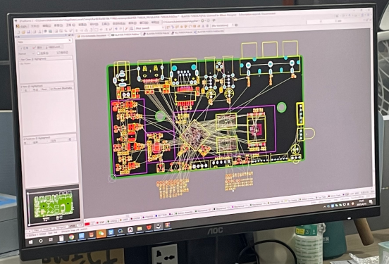
Tools and Software for Minimal PCB Design: Modern PCB design software can assist in navigating these complexities. Tools like Altium Designer, Autodesk Eagle, and KiCad provide advanced features for optimizing PCB layouts. These tools can help streamline the design process by enabling simulations, checking for signal integrity, and efficiently managing component placement to ensure that minimalism does not interfere with functionality. Some software also includes libraries of multi-functional ICs or SoCs that are ideal for minimalist designs.
By utilizing advanced design tools, engineers can create minimalist PCBs that still meet all technical requirements, reducing the risk of functional compromises.
Component Limitations
A significant challenge in minimalist PCB design is the potential trade-offs that come with using fewer components. While reducing the number of components can simplify the design and lower costs, it may also limit the functionality or performance of the PCB.
Potential Trade-offs of Fewer Components: Minimalist designs may require more powerful components to handle multiple functions, which can lead to heat dissipation issues or increase power consumption. For example, using a single multi-functional IC to replace several separate components may save space, but it could also put greater stress on the component, leading to potential reliability concerns.
Solutions: Multi-functional ICs and System-on-Chip (SoC) Designs: One solution to this challenge is the adoption of multi-functional ICs and SoC designs. A multi-functional IC integrates several functions, such as power management, signal processing, and wireless communication, into a single chip. This reduces the number of components, but the chip must be robust enough to handle multiple tasks without overheating or malfunctioning. System-on-Chip (SoC) solutions take this concept further by embedding an entire system—such as a processor, memory, and input/output controls—into one chip, streamlining the design and minimizing the need for multiple separate components.
Example:
In smartphones, using an SoC allows manufacturers to integrate the processor, GPU, memory, and even wireless communication functions into one chip. This minimizes the PCB size and complexity while maintaining the functionality required for modern smartphones.
Manufacturing Constraints
Minimalist designs present specific manufacturing challenges. While these designs reduce size and complexity, they often require specialized manufacturing processes to ensure that the final product meets both performance and quality standards.
How Minimal Layouts Affect Assembly Processes: Minimal layouts typically mean fewer components, but they can also lead to tighter component placement and routing. This requires more precision during assembly, as components must be placed more closely together without compromising electrical integrity. The manufacturing process may also need to be adapted to accommodate these compact designs, which can increase production complexity and costs.
Examples of Advanced PCB Fabrication Techniques Supporting Minimalism: Advanced PCB fabrication techniques have been developed to meet the demands of minimalist designs. For example, high-density interconnect (HDI) technology allows for the creation of PCBs with finer traces and smaller vias, enabling higher component density on a smaller board. Flexible PCBs and rigid-flex PCBs are also used to reduce the overall size and allow for more intricate designs that maintain functionality while being compact. Techniques such as laser direct imaging (LDI) help achieve the high precision needed for these complex, minimalist designs.
Example:
A smartwatch PCB might use HDI technology to place components densely, ensuring the device remains thin and lightweight without sacrificing performance. Similarly, rigid-flex PCBs can be used in wearable devices to achieve flexibility while maintaining the integrity of the circuit layout.
While minimalist PCB designs offer significant advantages in terms of size, cost, and performance, they also present challenges related to design complexity, component limitations, and manufacturing constraints. However, with the use of advanced design tools, multifunctional components, and specialized fabrication techniques, these challenges can be addressed, allowing for the continued evolution of smaller, more efficient, and highly functional electronic devices.
Future Outlook
Industry Trends
The trend toward minimalist circuit boards (PCBs) is rapidly expanding across various electronics sectors. As device miniaturization continues to accelerate, industries are increasingly adopting minimalist PCB designs to improve efficiency, reduce costs, and enhance product performance.
Adoption of Minimal PCBs Across Electronics Sectors: Minimalist PCB designs are no longer limited to just smartphones or wearables. Consumer electronics, industrial systems, and medical devices are also embracing the benefits of compact and efficient PCBs. As demand grows for smaller, more powerful devices across multiple industries, minimalist designs are becoming the standard. For example, in consumer electronics, companies are integrating minimalist PCBs into smart TVs, laptops, and home appliances, resulting in thinner, lighter, and more energy-efficient products.
Predictions for Next-Generation Electronics Designs: Looking ahead, we can expect next-generation electronics to rely heavily on minimalist PCBs. 5G technology, autonomous vehicles, and advanced medical devices will drive the need for even more compact and efficient circuit boards. As consumer demand for IoT devices, wearables, and flexible electronics increases, PCB designs will continue to evolve, focusing on further miniaturization without compromising functionality or performance. By 2030, it’s likely that multi-functional ICs and system-on-chip (SoC) solutions will dominate, integrating more capabilities into smaller footprints.
Role of AI and Automation
Artificial Intelligence (AI) and automation are playing a transformative role in PCB design, especially in optimizing layouts for minimalist designs. These technologies are helping designers tackle the challenges of fitting more functionality into smaller, more efficient PCBs.
Using AI-Driven PCB Design Tools for Optimized Layouts: AI-powered PCB design tools, such as Altium Designer and Autodesk Eagle, leverage machine learning to automate the process of optimizing layouts. These tools can suggest the most efficient placement for components, ensure minimal trace lengths, and even predict potential design flaws before the physical prototype is created. AI algorithms can analyze vast amounts of design data and recommend improvements, helping designers achieve the perfect balance between minimalism and performance.
Step-by-Step: AI-Assisted Minimal Trace Routing:
1. Input the Initial Design: The designer uploads the initial schematic into the AI-powered PCB design tool.
2. AI Optimization: The tool analyzes the design and suggests optimal component placements that minimize trace lengths while avoiding interference or signal degradation.
3. Automatic Routing: AI algorithms automatically route the traces, minimizing the number of layers and the length of each trace. This reduces manufacturing complexity and enhances signal integrity.
4. Simulation and Testing: The AI tool simulates the final design, checking for potential electrical or thermal issues.
5. Final Adjustments: The tool presents suggestions for any necessary adjustments, such as component swaps or trace rerouting, to improve efficiency and performance.
AI-driven tools are helping to accelerate the design process, reduce human error, and ensure that minimalist PCBs meet the demanding requirements of modern electronics.
Sustainability and Environmental Impact
As environmental concerns continue to grow, minimalist PCB designs present an opportunity to create more sustainable and eco-friendly electronics. Reducing the number of components and materials used in PCB design not only lowers production costs but also minimizes the environmental impact of electronics manufacturing.
Reduced Material Use → Greener Electronics: One of the most significant sustainability advantages of minimalist PCBs is the reduced material usage. By eliminating unnecessary components and simplifying the design, manufacturers can lower the overall amount of raw materials required for production. This reduction in material consumption contributes to a lower carbon footprint and less electronic waste, which is critical in the context of growing concerns over e-waste management.
Potential for Recycling-Friendly Minimalist PCBs: The trend toward minimalist PCBs also opens up new possibilities for recycling-friendly designs. With fewer materials and more standardized components, these PCBs are easier to disassemble and recycle. For example, the use of lead-free solder and biodegradable materials in minimalist designs can make it easier for manufacturers to recycle PCBs at the end of a product's life cycle, reducing the environmental impact. Flexible PCBs are also being explored as a potential solution for recyclable, eco-friendly electronics, as they can be made from materials that are both lightweight and recyclable.
Example:
In wearables like fitness trackers, minimalist PCBs not only help in creating compact, high-performance devices but also make recycling easier due to their simpler design and fewer layers. As these devices become more popular, the adoption of eco-friendly, minimalist PCBs will likely play a significant role in reducing the overall environmental footprint of wearable tech.
The future of minimalist PCB design is bright, with industry trends pointing toward broader adoption across electronics sectors. The integration of AI-driven design tools and the growing focus on sustainability will continue to shape the next generation of PCBs. As technologies evolve, minimalist designs will help drive more efficient, compact, and eco-friendly electronics, paving the way for innovation while reducing environmental impact.
Conclusion
Minimalist PCBs are revolutionizing the way we design and manufacture electronic devices, offering benefits in cost efficiency, performance, and sustainability. As industries across the board embrace this design philosophy, the role of advanced tools, AI, and sustainable practices will only grow. At PCBMASTER, we are committed to leading the charge in providing cutting-edge PCB solutions that not only meet the evolving demands of modern electronics but also contribute to a greener future. Whether you're looking for efficient designs for consumer electronics, industrial systems, or emerging technologies, PCBMASTER is here to help you innovate and succeed in the rapidly changing world of PCB manufacturing.
FAQs
What makes a circuit board “minimalist” compared to traditional PCBs?
A minimalist PCB is designed with simplicity in mind, focusing on reducing the number of components and layers while still meeting functional requirements. Unlike traditional PCBs, which may use multiple components for different functions, minimalist PCBs often incorporate multi-functional integrated circuits (ICs) or system-on-chip (SoC) solutions to consolidate tasks. Additionally, minimalist designs use shorter traces, fewer layers, and optimized component placements to reduce complexity and improve efficiency. This approach results in smaller, more compact boards with fewer materials.
How does a minimalist PCB design affect product performance?
Minimalist PCB designs can enhance product performance in several ways. By reducing the number of components, the risk of failure points decreases, making the device more reliable. Furthermore, simplified trace routing reduces signal interference and noise, leading to improved signal integrity and faster data transmission. The compact design also makes it easier to manage heat dissipation and power distribution, which is crucial for high-performance devices. While minimalist designs focus on efficiency, they still meet the necessary functional requirements, resulting in both high performance and compactness.
Can minimalism be applied to complex multi-layer PCBs?
Yes, minimalism can be applied to complex multi-layer PCBs. The key is to simplify the design by optimizing component placement and routing. For instance, high-density interconnect (HDI) technology can be used to reduce the number of layers while maintaining the PCB’s complexity. In such designs, multi-functional ICs or SoCs are often utilized to consolidate several components into one, reducing the overall board complexity. While multi-layer PCBs are typically needed for high-performance or intricate designs, minimalist principles can still help reduce the number of layers, streamline the routing, and cut down on excess components.
What industries benefit most from minimalist circuit board prints?
Several industries benefit significantly from minimalist circuit board designs:
Consumer Electronics: Products like smartphones, tablets, and wearables require small, lightweight PCBs with high performance. Minimalist designs allow for sleeker devices with longer battery life and improved functionality.
Medical Devices: Compact and efficient PCBs are essential for portable medical devices, such as wearable health monitors and implantable sensors. Minimalist designs help ensure that these devices are both reliable and small enough to fit into tight spaces.
Industrial Electronics: IoT sensors and other industrial equipment benefit from minimalist PCBs as they reduce size and complexity while enhancing performance and durability in harsh environments.
Aerospace and Defense: Lightweight and high-performance PCBs are critical in aerospace applications. Minimalist designs help meet the demands for smaller, lighter devices without compromising reliability or functionality.
Are there any software tools specifically for designing minimalist PCBs?
Yes, several PCB design software tools are optimized for creating minimalist designs. Tools such as Altium Designer, Autodesk Eagle, and KiCad allow engineers to design efficient, compact boards. These tools offer features like automated routing, multi-functional component libraries, and simulation capabilities, making it easier to reduce component count and optimize layout. Additionally, AI-powered tools are increasingly being used to automatically suggest efficient design choices, further simplifying the process of creating minimalist PCBs.

