


High-Complexity PCB Manufacturing: Key Technologies, Applications, and Benefits
High-performance technologies demand more than just conventional components—they require precision, durability, and complexity. As electronics evolve, so too must the circuit boards that power them. High-complexity PCBs are at the heart of groundbreaking innovations, from self-driving cars to cutting-edge medical devices, where every millimeter counts and every signal matters. These advanced boards push the limits of design and engineering, enabling solutions that were once thought impossible. But what does it take to create such high-performance PCBs, and why are they so critical to the technologies of tomorrow? Let’s dive into the world of high-complexity PCB manufacturing and uncover what makes these components so vital for the future of electronics.
Introduction to High-Complexity PCB Manufacturing
What is High-Complexity PCB?
High-complexity PCBs (Printed Circuit Boards) are specialized circuit boards designed to meet the demanding needs of modern, high-performance technologies. Unlike standard PCBs, which typically feature fewer layers and simpler components, high-complexity PCBs are characterized by their multi-layered structures, miniature components, and intricate routing. These boards are engineered to handle dense component layouts, advanced signal processing, and stringent environmental conditions.
Key characteristics of high-complexity PCBs include:
Layer Count: Often 16 layers or more, allowing for more compact designs and improved signal integrity.
Component Pitch: Smaller component pitches, sometimes as fine as 0.25mm, enable the integration of highly dense circuits.
Material Diversity: These PCBs may use advanced materials like ceramic, polyimide, or metal cores, which offer superior heat dissipation and resistance to extreme conditions.
In short, high-complexity PCBs are integral to applications where traditional PCBs would struggle due to the need for greater performance, space efficiency, and durability.
Importance in Advanced Electronics:
High-complexity PCBs are at the heart of some of the most groundbreaking technologies today. For example, in autonomous vehicles, these PCBs handle the high-speed signals required for real-time decision-making, sensor fusion, and communication between vehicle components. In the field of medical devices, such as wearable health monitors or diagnostic equipment, high-complexity PCBs are critical for ensuring compact designs that are both reliable and capable of withstanding challenging environmental factors like temperature fluctuations and moisture.
The Need for High-Complexity PCBs in Modern Technology
As technology continues to evolve, the demand for high-complexity PCBs has surged. These advanced circuit boards are no longer just an option—they are a necessity. The key to their rise lies in the ever-increasing performance requirements and miniaturization trends across multiple industries.
Industries Relying on High-Complexity PCBs:
Automotive: With the growth of autonomous and electric vehicles, advanced PCBs are required to support high-speed data transfer, intricate sensor systems, and communication modules.
Medical Devices: Devices such as pacemakers, diagnostic equipment, and wearable health trackers require compact, highly reliable PCBs that can function under harsh conditions.
Consumer Electronics: The need for faster, more powerful devices (like smartphones, smartwatches, and wearables) demands the integration of high-complexity PCBs that support miniaturization without compromising performance.
Aerospace and Defense: With strict safety and reliability requirements, aerospace systems depend on high-complexity PCBs for mission-critical applications that must function flawlessly in extreme conditions.
Key Drivers of Demand:
Miniaturization: As devices become smaller, there is less space for components, demanding more complex and efficient PCB designs. High-complexity PCBs enable tighter layouts, allowing for greater functionality in a smaller footprint.
High-Speed Performance: The increasing need for faster data transmission—whether in telecommunications, computing, or automotive systems—requires PCBs that can handle high-frequency signals with minimal interference.
Environmental Resilience: Many modern applications, especially in aerospace, automotive, and medical fields, require PCBs that can withstand harsh environments, such as extreme temperatures, vibrations, and exposure to chemicals. Advanced materials and design techniques used in high-complexity PCBs ensure they can perform reliably under such conditions.
In summary, the growing reliance on high-complexity PCBs reflects the relentless pace of technological advancement. Their ability to meet the demands of smaller sizes, higher speeds, and extreme durability makes them indispensable in driving the future of electronics.
Key Features of High-Complexity PCBs
Layer Count and Design Complexity
Comparison with Standard PCBs:
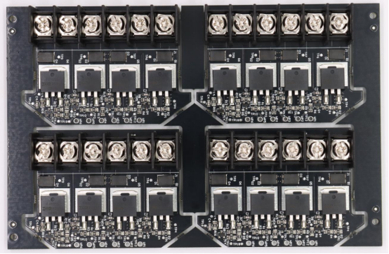
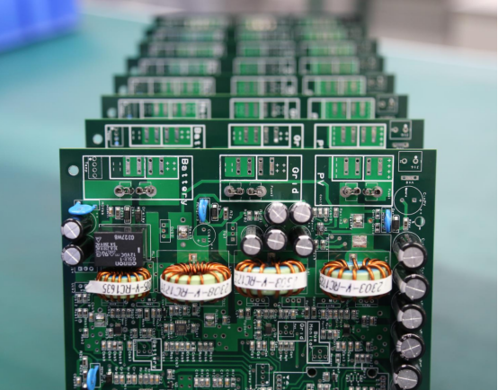
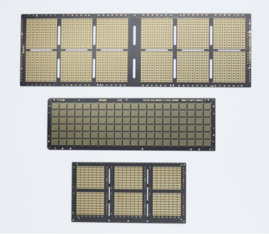
One of the defining characteristics of high-complexity PCBs is their layer count. While standard PCBs typically feature between 4 to 8 layers, high-complexity PCBs often contain 16 or more layers, and some can even exceed 24 layers. This additional complexity allows for more dense circuit designs, enabling higher functionality and performance in a smaller footprint.
Benefits of Multi-Layer PCBs in Dense Applications:
The increase in layers offers several advantages, particularly in dense applications where space is limited. Each layer in a high-complexity PCB serves a specific purpose—whether it's for routing signals, grounding, or powering components—while ensuring that signals are routed in the most efficient and interference-free manner. Multi-layer boards also improve signal integrity, as the inner layers can be used for grounding or power distribution, reducing noise and crosstalk.
In applications such as smartphones, automotive electronics, or high-speed communications, multi-layer PCBs are essential for packing more functionality into a smaller device. This enables innovations in miniaturization without sacrificing performance.
Material Types and Selection
Common vs. Advanced Materials (FR-4 vs. Ceramic, Polyimide, Metal Core):
High-complexity PCBs are often made from advanced materials that provide specific benefits for demanding applications. The most commonly used material in standard PCBs is FR-4 (a fiberglass-reinforced epoxy laminate), which is cost-effective and sufficient for basic designs. However, high-complexity PCBs require more specialized materials like:
Ceramic: Offers excellent heat resistance and is ideal for high-power applications.
Polyimide: A flexible material used in flexible PCBs that can withstand higher temperatures and mechanical stress.
Metal Core: Primarily used in LED lighting and high-power electronics, metal core PCBs provide superior heat dissipation compared to traditional materials.
Each material has its specific use case and provides unique advantages depending on the requirements of the application, such as thermal conductivity, flexibility, or mechanical stability.
Role of Material Choice in PCB Performance and Reliability:
The material selection directly impacts the performance and reliability of the PCB. For example, ceramic PCBs are often chosen for high-frequency or high-power applications due to their superior heat resistance and ability to maintain signal integrity under harsh conditions. Polyimide, being highly flexible, is crucial for rigid-flex applications where the PCB needs to bend or be shaped to fit into tight spaces, like in wearable electronics. By selecting the appropriate material, manufacturers can ensure that the PCB performs well under specific operational conditions, such as extreme temperatures, vibrations, or electrical stresses.
Size and Component Density
Smaller Component Pitch (0.25mm vs. 0.5mm):
As technology advances, the need for more compact electronics has led to smaller component pitches, which refer to the distance between the centers of adjacent components. In standard PCBs, the component pitch is typically around 0.5mm or larger, but in high-complexity PCBs, the pitch can be as small as 0.25mm. This reduction allows for more components to be packed into the same area, making the PCB smaller and more functional.
Impact on Board Functionality and Compactness:
Smaller component pitches and increased component density enable the design of more compact and feature-rich PCBs. This is particularly beneficial in industries where space is at a premium, such as in consumer electronics, medical devices, or aerospace. The smaller size does not mean sacrificing performance; rather, it enhances the board’s functionality by allowing additional features like more sensors, processors, or communication modules to be integrated into the design.
For example, in smartphones and wearables, the PCB must house a variety of sensors, chips, and connectors while maintaining a slim form factor. The ability to reduce component pitch makes this possible, allowing manufacturers to achieve higher functionality in increasingly smaller devices.
In summary, the key features of high-complexity PCBs—layer count, material selection, and component density—allow for more advanced, smaller, and efficient designs. These features are critical in driving the innovation seen in modern electronics, where performance, reliability, and miniaturization are paramount.
Advanced Technologies in High-Complexity PCB Manufacturing
High-Density Interconnect (HDI) Technology
Overview of Micro-Via Technology:
High-Density Interconnect (HDI) technology is a crucial advancement in PCB manufacturing that enables the creation of highly compact, high-performance boards. The core feature of HDI is the use of micro-vias—very small holes drilled into the PCB to connect different layers. These micro-vias typically range from 50μm to 30μm in diameter, enabling much higher component density than traditional via designs.
Micro-via technology allows manufacturers to build multi-layer PCBs with more intricate connections, which is essential for modern applications where space is limited, but performance demands are high. By using HDI, manufacturers can create more compact, faster, and more efficient circuit boards, which are key to powering advanced electronics like smartphones, wearables, and aerospace systems.
Applications in Smartphones, Wearables, and Aerospace:
In smartphones and wearable devices, where space is at a premium, HDI technology allows for the integration of more features into smaller form factors. The micro-vias enable compact routing and efficient signal management, contributing to enhanced performance in devices like smartwatches, fitness trackers, and headphones. In aerospace applications, HDI technology is used to create lightweight, high-reliability PCBs for communication and control systems, where small size and high performance are critical.
Industry Comparison: HDI Capabilities from 50μm to 30μm:
Compared to traditional PCBs, which use larger vias (100μm or more), HDI PCBs can incorporate much finer micro-vias, ranging from 50μm to 30μm in diameter. This reduction in via size allows for a higher component density, faster signal transmission, and better thermal performance. For example, in 5G telecommunications and autonomous vehicles, where speed and signal integrity are essential, the use of HDI technology provides a significant performance edge.
Rigid-Flex PCB Manufacturing
Combining Rigidity and Flexibility for Specialized Applications:
Rigid-flex PCBs combine the best aspects of both rigid and flexible circuit boards. These boards have rigid sections that provide structural support and flexible sections that allow the board to bend and conform to tight spaces. The combination offers greater design flexibility while maintaining the reliability and durability of traditional rigid PCBs.
Rigid-flex technology is particularly useful in applications where the PCB needs to fit into non-flat spaces or endure mechanical stress without compromising performance. These PCBs are widely used in industries where durability and compactness are key, such as medical devices, and aerospace.
Use Cases: Medical Devices, Aerospace:
Medical Devices: In medical devices like implantable devices or wearable health monitors, rigid-flex PCBs offer compactness and reliability. They allow devices to conform to the body while providing long-lasting durability, even in harsh environments.
Aerospace: In aerospace systems, rigid-flex boards are used to power navigation systems, communication satellites, and unmanned aerial vehicles (UAVs), where size, weight, and flexibility are crucial for operational success.
Rigid-Flex vs. Traditional PCBs: Benefits and Drawbacks:
While rigid-flex PCBs offer unmatched design flexibility, they do come with some trade-offs. Compared to traditional rigid PCBs, rigid-flex designs are generally more expensive due to the additional manufacturing steps and materials required. However, their compactness and ability to withstand mechanical stress make them ideal for space-constrained, mission-critical applications. Traditional PCBs, on the other hand, are more cost-effective and simpler to produce but lack the flexibility that modern designs often demand.
3D PCB Assembly Techniques
Vertical Stacking and Its Impact on Space Optimization:
3D PCB assembly techniques involve vertical stacking of components, allowing multiple layers of circuits to be stacked on top of one another rather than spread across a flat board. This approach greatly optimizes space utilization, enabling the creation of smaller, more powerful PCBs. By using this method, manufacturers can achieve a higher component density while still maintaining performance and reliability.
This technique is especially beneficial in applications where compact size is critical, such as high-performance computing systems, telecommunications, and consumer electronics. The ability to stack components vertically enables designers to create boards with multiple functional layers, each serving a different purpose, without increasing the physical footprint of the device.
Example Applications: Telecommunications, High-Performance Computing:
Telecommunications: In high-speed networks and 5G infrastructure, 3D assembly techniques are used to produce compact, efficient PCBs that can handle large amounts of data transmission and processing in a small form factor.
High-Performance Computing: 3D PCB assembly is widely used in servers and data centers, where speed, efficiency, and reduced latency are critical. Vertical stacking allows for the integration of more components, such as processors and memory, without compromising the overall system's size or cooling performance.
In conclusion, advanced manufacturing technologies like HDI, rigid-flex, and 3D assembly are transforming PCB design and production. These innovations enable manufacturers to create more compact, efficient, and high-performance PCBs that are essential for the next generation of electronics. Whether it's wearables, aerospace systems, or 5G networks, these technologies play a crucial role in meeting the growing demands of modern technology.
The Manufacturing Process of High-Complexity PCBs
Design for Manufacturability (DFM)
Role of DFM in Reducing Design Errors and Optimizing Cost:
Design for Manufacturability (DFM) is a critical process in high-complexity PCB manufacturing. DFM ensures that a PCB design is optimized for production, minimizing potential errors and reducing costs during the manufacturing phase. By identifying design flaws early on, such as improper component spacing or incompatible materials, engineers can avoid costly revisions and delays. This proactive approach leads to faster production times and more efficient use of resources.
For example, a design that’s optimized for manufacturability can reduce the need for expensive rework or re-testing, which ultimately lowers overall production costs and ensures that the final product meets the required specifications without unnecessary complexity.
Collaboration with Engineers from Design to Production:
DFM is most effective when there is close collaboration between designers and engineers throughout the entire process. Early involvement of manufacturing engineers during the design phase ensures that all elements of the PCB are optimized for production feasibility. Engineers provide valuable feedback on material selection, component placement, and layer stacking, helping to refine the design for better performance and manufacturability. This collaboration not only reduces errors but also ensures that the final product can be produced efficiently and meets all the technical requirements.
Prototyping and Testing
Steps Involved in PCB Prototyping:
Prototyping is a crucial phase in high-complexity PCB manufacturing. It allows engineers to create an initial version of the board, test its functionality, and identify any issues before moving to full-scale production. The process typically includes:
1. Design Finalization: Once the design is completed, it is converted into files that specify the layout, components, and electrical connections.
2. Fabrication: The prototype PCB is manufactured using the specified materials and techniques.
3. Assembly: Components are soldered onto the board, following the finalized design.
4. Initial Testing: The board is powered on and tested for basic functionality.
Prototyping is particularly important in high-complexity PCBs, where even small design issues can lead to significant performance problems. It allows manufacturers to validate the design’s performance and make necessary adjustments.
Common Testing Methods (AOI, X-ray, Flying Probe Test):
Several testing methods are used to ensure that high-complexity PCBs meet quality and performance standards:
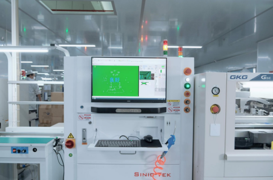
Automated Optical Inspection (AOI): AOI uses cameras to scan the PCB for visual defects, such as misaligned components or soldering issues. This is an essential step for identifying errors quickly.
X-ray Inspection: X-ray machines are used to inspect internal layers and hidden solder joints in complex, multi-layered PCBs. This method ensures that there are no hidden defects that could affect performance.
Flying Probe Testing: Flying probes are used to test electrical connections and ensure that all circuits are properly connected. This method is particularly useful for small-volume production and prototypes.
Speed and Accuracy of Prototyping in High-Complexity Projects:
In high-complexity PCB manufacturing, rapid prototyping is vital. The ability to produce accurate prototypes quickly allows designers to test and iterate their designs faster, reducing the time to market. Advanced prototyping techniques enable manufacturers to produce functional prototypes within a few days, ensuring that design adjustments can be made before moving to full-scale production. This speed and accuracy are especially important in industries like medical devices, telecommunications, and automotive electronics, where rapid development cycles are crucial.
Mass Production and Scalability
Transition from Prototypes to Large-Scale Production:
Once the prototype is tested and verified, the next step is to transition to mass production. This process involves scaling the design from a small number of prototypes to hundreds or thousands of units. The shift from prototype to production requires careful planning to ensure that production processes are repeatable and consistent. Adjustments may need to be made to the assembly line setup, material procurement, and testing procedures to handle larger volumes while maintaining the same level of quality.
Ensuring Quality Consistency in High-Volume Runs:
One of the challenges of mass production is maintaining consistent quality across large batches. High-complexity PCBs require precision at every step, from component placement to soldering. To ensure consistency, manufacturers rely on strict quality control measures, such as automated inspections and statistical process controls. These tools help identify any variations or defects in the production line before they become widespread issues. The goal is to maintain the integrity and performance of each PCB, ensuring that every unit meets the required specifications.
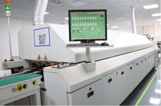
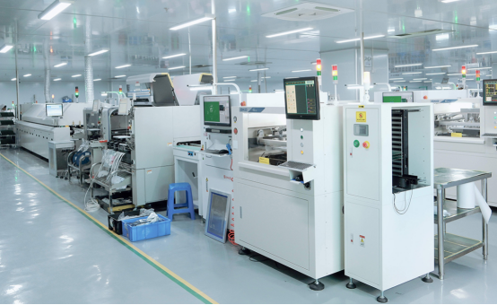
Automation in Production for Speed and Precision:
To meet the high demand for high-complexity PCBs, manufacturers increasingly turn to automation to speed up production while maintaining precision. Automated machines can handle tasks such as soldering, component insertion, and inspection more quickly and accurately than manual labor, leading to faster turnaround times and fewer errors. Automation also helps to reduce the risk of human error and ensures that production runs are highly consistent. With automation, manufacturers can scale production without sacrificing quality or increasing costs significantly.
In summary, the manufacturing process of high-complexity PCBs involves several crucial stages, including Design for Manufacturability (DFM), prototyping and testing, and mass production. Each phase plays a vital role in ensuring that the final product meets the stringent requirements of modern electronics. By employing advanced techniques and maintaining close collaboration between designers and engineers, manufacturers can produce high-quality, reliable PCBs that power the next generation of technology.
Ensuring Quality and Reliability in High-Complexity PCBs
Advanced Quality Control Measures
Comprehensive Inspection Techniques (AOI, X-ray, Flying Probe):
Ensuring the quality of high-complexity PCBs requires advanced inspection techniques throughout the manufacturing process. The most commonly used methods include:
Automated Optical Inspection (AOI): AOI is used to visually inspect the PCB for issues like misaligned components, soldering defects, or broken connections. Cameras scan the board, comparing it to the design files to detect even the smallest flaws, such as misplacement or solder bridges.
X-ray Inspection: X-ray inspection is crucial for multi-layer PCBs where internal layers and connections need to be examined. It is especially useful for detecting hidden defects such as voids or insufficient soldering in areas that cannot be easily accessed by other means.
Flying Probe Test: The flying probe test is a method that uses multiple probes to electrically test the connections of the PCB. It’s highly effective for checking continuity, short circuits, and component placement in small-volume or prototype runs.
How Defects Are Detected and Prevented at Each Manufacturing Stage:
Defects can arise at various stages of PCB manufacturing, from design to final assembly. Quality control measures are designed to detect and prevent these defects early in the process:
1. Design Validation: During the design phase, Design for Manufacturability (DFM) guidelines help ensure the design is feasible for mass production. This reduces the likelihood of design errors later in the process.
2. Fabrication Checks: During fabrication, automated inspection tools like AOI identify issues such as misalignment or poorly etched traces.
3. Assembly Inspection: Once components are placed, X-ray and flying probe tests ensure that all internal connections and component placements are accurate and functioning.
4. Final Inspection: At the end of the production line, a final round of AOI and electrical testing ensures that the PCB is free from defects and meets performance requirements.
By using a combination of these advanced inspection techniques, manufacturers can catch defects early, reducing the need for costly rework and ensuring that the final product meets quality standards.
Certifications and Standards
ISO 9001, ISO 13485, UL Certifications and Their Significance:
Certifications are a critical part of ensuring the quality and reliability of high-complexity PCBs. Key certifications include:
ISO 9001: This standard focuses on quality management systems (QMS) and ensures that manufacturing processes consistently meet customer requirements. It guarantees that a company adheres to international standards for quality control, production, and continuous improvement.
ISO 13485: Specifically designed for the medical device industry, this certification ensures that PCBs used in medical devices meet stringent regulatory standards for safety, reliability, and performance. It demonstrates a commitment to maintaining high quality in the design, development, and production of PCBs for healthcare applications.
UL Certification: UL (Underwriters Laboratories) certification ensures that PCBs meet safety standards for electrical components. It is particularly important for ensuring that the PCBs are safe to use in products where electrical hazards may be a concern, such as in consumer electronics or automotive applications.
Ensuring Compliance with International Standards for Specific Industries:
For high-complexity PCBs used in specialized industries such as aerospace, medical devices, and automotive electronics, compliance with industry-specific standards is essential. For example, aerospace PCBs must adhere to AS9100 standards, which focus on the quality and safety of components used in flight systems. Similarly, automotive PCBs often need to meet IATF 16949 standards to ensure that the components can handle the harsh conditions of automotive environments, such as extreme temperatures and vibrations.
By adhering to these international certifications and standards, manufacturers can guarantee that their products not only meet customer expectations but also comply with regulatory requirements in the relevant industries.
Traceability and Documentation
Importance of Material and Process Traceability:
Traceability refers to the ability to track the origin and history of every component and material used in PCB manufacturing. This is crucial for ensuring that each PCB meets the required standards of performance and reliability. Traceability also enables manufacturers to pinpoint the exact source of any issues, whether they arise from the raw materials or during the manufacturing process.
By maintaining detailed records of materials, component batches, and processes used at every stage, manufacturers can ensure full accountability and prevent faulty products from reaching the market. This transparency is especially important for high-reliability industries like aerospace or medical devices, where a single defect could lead to catastrophic failure.
How Traceability Supports Regulatory Compliance and Product Reliability:
In regulated industries, traceability is not just about ensuring product quality; it’s also a key part of regulatory compliance. For example, in the medical device industry, traceability allows manufacturers to demonstrate that their products comply with strict FDA and ISO 13485 requirements. If a product recall is necessary, traceability makes it possible to quickly identify and remove affected units from the supply chain.
Moreover, detailed documentation and traceability can improve product reliability by allowing manufacturers to continuously monitor the performance of materials and components over time. If issues arise, the ability to trace each component’s journey through the production process helps to identify where problems originated and prevent future occurrences.
In conclusion, ensuring the quality and reliability of high-complexity PCBs involves a comprehensive approach that includes advanced quality control measures, adherence to international standards, and maintaining traceability throughout the manufacturing process. These practices help manufacturers deliver products that meet the highest performance standards while ensuring compliance with the most stringent regulatory requirements.
Applications of High-Complexity PCBs in Various Industries
Automotive and Autonomous Vehicles
Use of High-Complexity PCBs in Autonomous Driving Systems:
High-complexity PCBs are essential for the advanced technology in autonomous vehicles. These vehicles rely on multiple interconnected systems like LiDAR, radar sensors, cameras, and control systems, all of which require reliable, high-performance PCBs to ensure safety and efficiency. The complexity of autonomous driving systems requires PCBs that can handle high-speed data transfer, precise signal processing, and environmental durability.
Case Study: PCB for a Self-Driving Vehicle’s Sensor and Control Systems:
In one project for a self-driving vehicle, our client needed a multi-layered PCB that would support the vehicle's sensor and control systems, including object detection, motion control, and sensor fusion. This PCB had to process high volumes of real-time data from radar and LiDAR sensors to make instant driving decisions.
A rigid-flex design was chosen to optimize the limited space in the vehicle’s sensor suite while providing the necessary flexibility for mounting in curved areas. The PCB also utilized high-density interconnect (HDI) technology to manage the complex data pathways while minimizing space. Rigorous testing ensured the final product met all operational standards, resulting in a highly reliable and compact PCB suitable for autonomous driving applications.
Medical Devices and Healthcare
Role of Rigid-Flex and Miniaturized PCBs in Medical Devices:
High-complexity PCBs are indispensable in the medical device sector, where size, durability, and reliability are critical. Rigid-flex PCBs combine the benefits of rigid boards for structural integrity with flexible sections that conform to compact or irregular spaces. These PCBs are commonly used in devices such as wearable health monitors, implantable sensors, and portable diagnostic tools.
The ability to miniaturize the PCB while maintaining high functionality allows manufacturers to create more compact, lightweight, and efficient devices, all of which are crucial in improving patient care and outcomes.
Case Study: PCB for a Portable Diagnostic Tool:
A prominent healthcare company required a miniaturized PCB for a portable diagnostic tool designed to monitor heart rate and oxygen levels in patients. The device needed to be lightweight, accurate, and capable of operating in various environments, from hospitals to remote areas.
A rigid-flex design was employed to ensure flexibility, while the HDI technology minimized the PCB size while maintaining high connectivity. The result was a compact, portable, and reliable diagnostic tool that allowed the company to meet the growing demand for home healthcare solutions and improve patient access to monitoring technology.
Aerospace
Extreme Environmental Conditions and the Need for Reliable PCBs:
In aerospace, PCBs must operate under extreme conditions, such as high altitudes, temperature fluctuations, and radiation exposure. These environmental factors require high-reliability PCBs that can withstand physical stresses without compromising performance. The ability to maintain signal integrity and thermal stability is crucial for systems like satellite communication and navigation.
For example, PCBs used in satellites need to function perfectly in space, where temperature extremes, vacuum conditions, and radiation can degrade components if not properly designed.
Case Study: PCB for a Satellite Communication System:
A client in the aerospace industry required a high-performance PCB for a satellite communication system. This PCB had to endure extreme temperatures, radiation, and the vacuum of space, all while maintaining stable communication links between the satellite and ground stations.
To meet these stringent demands, the PCB was designed with advanced materials such as ceramic and polyimide to enhance thermal stability and mechanical durability. The use of HDI technology allowed for high-density components and minimal space usage, crucial for the compact nature of space-bound devices. The final product successfully passed all environmental testing, ensuring reliability in the most demanding aerospace conditions.
In conclusion, high-complexity PCBs are integral to the success of industries like automotive, medical, and aerospace, where performance, reliability, and miniaturization are key. Whether for autonomous vehicles, portable medical devices, or space exploration, advanced PCB technologies such as HDI, rigid-flex designs, and miniaturization help these industries meet their exacting requirements and drive innovation in their respective fields.
Challenges in High-Complexity PCB Manufacturing
Managing Cost vs. Performance
Balancing the Need for Advanced Features with Cost Considerations:
One of the primary challenges in high-complexity PCB manufacturing is striking the right balance between advanced features and cost efficiency. High-complexity PCBs, such as those used in autonomous vehicles, medical devices, and aerospace, often require multi-layered designs, HDI technology, and specialized materials like ceramic and polyimide. These advanced features improve the performance and reliability of the PCB but also increase production costs due to higher material expenses, complex fabrication processes, and more stringent testing requirements.
For manufacturers, the challenge is to meet the high-performance standards required by the industry while keeping costs manageable. This balance is especially critical in high-volume production or in industries where cost-effectiveness is a key consideration without compromising product quality.
Strategies for Maintaining Cost-Effectiveness Without Sacrificing Quality:
Several strategies can help manufacturers control costs while maintaining the quality and performance of high-complexity PCBs:
1. Design for Manufacturability (DFM): Incorporating DFM principles early in the design phase helps reduce complexity by ensuring the PCB layout is optimized for efficient production. This can minimize design errors, rework, and unnecessary material use, ultimately lowering costs.
2. Selective Use of Advanced Materials: Not all sections of a high-complexity PCB require premium materials. By using advanced materials like polyimide or ceramic in specific areas where they are essential for performance, and opting for more cost-effective materials like FR-4 where appropriate, manufacturers can reduce costs without sacrificing critical features.
3. Efficient Production Processes: Adopting automation and advanced manufacturing technologies can significantly reduce labor costs and improve consistency in high-complexity PCB production. Automated Optical Inspection (AOI) and flying probe testing can also enhance testing efficiency, cutting down on inspection time and costs.
4. Prototyping and Testing: Speeding up prototyping and reducing iteration cycles can save both time and money. Leveraging rapid prototyping allows for quick iterations and testing, ensuring that issues are addressed early before scaling up to mass production.
By focusing on optimized designs, smart material choices, and production efficiency, manufacturers can keep costs under control while delivering high-performance, high-reliability PCBs.
Environmental and Sustainability Challenges
Sustainable Materials and Manufacturing Practices in PCB Production:
As the electronics industry grows, there is increasing pressure to address the environmental impact of manufacturing processes, including PCB production. High-complexity PCBs often involve the use of materials like epoxy resins, lead-based solder, and plastics, which can have negative environmental effects during their production and disposal.
The challenge for PCB manufacturers is finding alternatives that maintain the performance characteristics of high-complexity boards while reducing their environmental footprint. Sustainable materials such as lead-free solder, bio-based polymers, and recycled materials are gaining traction in PCB production. These materials can help mitigate the environmental impact without compromising the integrity of the final product.
The Push for Eco-Friendly Certifications and Waste Reduction:
To meet both regulatory requirements and growing consumer demand for sustainable products, manufacturers are adopting eco-friendly practices and pursuing certifications such as RoHS (Restriction of Hazardous Substances) and ISO 14001 for environmental management systems. These certifications ensure that PCB manufacturers meet stringent standards for hazardous substance management, recycling, and waste disposal.
RoHS Compliance: This directive restricts the use of harmful substances such as lead, mercury, and cadmium in the production of electronic products, including PCBs. Manufacturers must ensure their PCBs are RoHS-compliant to reduce environmental harm and promote recycling.
Waste Reduction: PCB production often generates significant waste, including scrap materials and chemical by-products. To combat this, manufacturers are adopting more efficient production methods, such as closed-loop systems that reduce waste and recycle materials. Zero-waste practices and reduced energy consumption during manufacturing processes are also becoming more prevalent.
Sustainable Manufacturing Processes: Advances in green technologies and eco-friendly chemicals are allowing manufacturers to reduce their reliance on toxic solvents and metals. Water-based etching processes and lead-free soldering are examples of how manufacturers are reducing the environmental impact of PCB production.
By integrating sustainable materials, adhering to eco-friendly certifications, and adopting waste-reduction strategies, manufacturers can address the growing demand for environmentally responsible PCBs without compromising performance.
In summary, cost management and environmental sustainability are two of the biggest challenges in high-complexity PCB manufacturing. Balancing cost-effectiveness with the need for advanced features requires strategic design, material selection, and production optimization. At the same time, addressing environmental concerns involves adopting sustainable practices, using eco-friendly materials, and achieving key industry certifications. Overcoming these challenges is crucial for maintaining competitive advantage and meeting the evolving demands of modern industries.
Future Trends in High-Complexity PCB Manufacturing
Innovations in PCB Materials
Future Advancements in Materials (e.g., Biodegradable PCBs):
The demand for environmentally friendly and sustainable solutions is driving innovations in PCB materials. One of the most promising developments is the potential for biodegradable PCBs. These PCBs are designed to reduce the environmental impact of electronic waste by breaking down more easily after their useful life, minimizing the accumulation of harmful materials in landfills.
In the future, we can expect to see more advanced materials, such as bioplastics and organic compounds, that retain the performance and reliability of traditional materials while offering better biodegradability and sustainability. Eco-friendly materials could also improve the recyclability of PCBs, making it easier to reuse components and reduce the need for raw materials.
Impact on PCB Durability and Environmental Impact:
The shift toward biodegradable and sustainable materials will also have a significant impact on the durability and environmental footprint of PCBs. While traditional PCBs are known for their robustness and longevity, biodegradable PCBs may not yet match these characteristics under extreme conditions. However, as material science advances, manufacturers are finding ways to improve the durability of eco-friendly materials, ensuring they can withstand the demands of modern applications, such as in autonomous vehicles, medical devices, and aerospace.
The broader adoption of sustainable materials will reduce the environmental harm caused by the disposal of PCBs and help the electronics industry move toward a more circular economy—where products are reused, recycled, and not just discarded.
Automation and AI in PCB Manufacturing
Role of AI in Design Optimization and Fault Detection:
Artificial Intelligence (AI) is rapidly transforming the landscape of PCB manufacturing, particularly in design optimization and fault detection. AI tools can help designers automatically optimize layouts to reduce space, improve signal integrity, and ensure that the design is DFM (Design for Manufacturability) compliant. By analyzing vast amounts of data from past designs, AI can predict potential issues before they arise, reducing the need for manual intervention and speeding up the design process.
In fault detection, AI can be used to analyze data from inspections, such as those performed with automated optical inspection (AOI), to detect defects or anomalies at much higher speeds and with greater accuracy than traditional methods. Machine learning algorithms can learn from previous testing results, continually improving their ability to identify subtle defects that might otherwise go unnoticed, ensuring higher quality control.
The Future of Automated Production Lines in PCB Manufacturing:
As PCB manufacturing becomes more complex, the role of automation will only continue to expand. In the future, fully automated production lines will be the norm, where machines handle everything from material handling and component placement to soldering and testing. This shift towards automation is driven by the need for faster production speeds, higher precision, and cost reductions.
Automated lines will not only improve manufacturing efficiency but also reduce human error, leading to a more consistent and high-quality product. Advanced robotics and smart factories will allow for real-time monitoring and optimization of production processes. For example, robots equipped with AI could monitor the production environment for temperature fluctuations, humidity changes, or material defects, instantly adjusting production parameters to prevent issues.
The integration of AI-driven automation will significantly enhance the scalability of high-complexity PCB production. Manufacturers will be able to quickly transition from small batch production to large-scale runs while maintaining the same level of precision and quality.
In conclusion, the future of high-complexity PCB manufacturing will be shaped by innovations in materials and the increasing integration of automation and AI. From biodegradable PCBs that reduce environmental impact to AI-powered design optimization and automated production lines, these advancements will enhance manufacturing efficiency, product performance, and sustainability. As the industry continues to evolve, these trends will help meet the growing demands of modern electronics while addressing the challenges of environmental responsibility and cost management.
Conclusion: Why Choose High-Complexity PCBs for Your Next Project?
High-complexity PCBs offer unmatched reliability, performance, and versatility in modern electronic applications. Whether you're designing for autonomous vehicles, medical devices, or high-performance computing, these advanced PCBs are engineered to meet the demands of today's technology. With multi-layer designs, HDI capabilities, and specialized materials, high-complexity PCBs ensure that your products are both compact and highly functional, without compromising on quality or performance.
When selecting a PCB manufacturer, it’s crucial to partner with an experienced provider who understands the intricacies of complex designs and can deliver customized solutions. Look for a manufacturer with advanced technological capabilities, a commitment to quality control, and the ability to scale from prototyping to high-volume production. A good partner will also collaborate closely with you during the design phase, ensuring that every aspect of the PCB is optimized for both manufacturability and performance.
At PCBMASTER, we specialize in providing cutting-edge PCB solutions and can help guide you through every step of the process, from design to mass production. If you have any questions or would like to explore your options for complex, custom PCBs, feel free to reach out to us anytime.
FAQs
What industries benefit most from high-complexity PCBs?
High-complexity PCBs are integral to several industries where performance, reliability, and miniaturization are critical. The automotive industry, particularly in autonomous vehicles, relies on high-complexity PCBs to manage the extensive sensor networks and high-speed data processing required for safe operation. Similarly, the medical device sector benefits from high-complexity PCBs used in implantable devices, wearable health monitors, and diagnostic equipment, where size, precision, and durability are paramount. Additionally, aerospace and telecommunications industries also require high-performance PCBs that can withstand extreme conditions while providing stable, high-speed communication and processing capabilities.
How does the design process differ for high-complexity PCBs compared to standard PCBs?
The design process for high-complexity PCBs differs significantly from standard PCBs in several key areas. First, high-complexity PCBs often require multi-layer designs, involving 16+ layers compared to the typical 4-8 layers of standard PCBs. This requires advanced stacking techniques and precise layer alignment to ensure electrical performance. The use of HDI (High-Density Interconnect) technology, micro-vias, and fine-pitch components also plays a major role in reducing the size of the PCB while enhancing performance. The design process for these boards involves careful consideration of thermal management, signal integrity, and manufacturability—all factors that are less critical in standard PCB designs. Moreover, DFM (Design for Manufacturability) is much more crucial for high-complexity PCBs to ensure that complex designs can be efficiently produced without defects.
What are the main challenges when manufacturing high-complexity PCBs?
The manufacturing of high-complexity PCBs presents several challenges. First, the complexity of the design itself requires more advanced materials and manufacturing techniques. For example, using materials like ceramic or polyimide adds to the difficulty and cost. Secondly, precision in layer alignment and minimizing defects in micro-vias and fine-pitch components is critical. Achieving this level of precision requires advanced equipment such as X-ray inspection, automated optical inspection (AOI), and flying probe testing. Additionally, cost management is a challenge, as these advanced manufacturing processes tend to be more expensive. Finally, scalability and production speed can also be challenging, as moving from prototyping to mass production without compromising quality requires highly automated and fine-tuned production lines.
What certifications should high-complexity PCBs have for medical device applications?
High-complexity PCBs used in medical device applications must meet rigorous certification standards to ensure safety, performance, and regulatory compliance. The most important certifications include ISO 13485, which ensures that the manufacturing processes meet the specific requirements of the medical device industry. This certification covers the entire lifecycle of a product, from design and development to production and distribution. ISO 9001, the general quality management standard, is also required to ensure consistent product quality. For certain devices, UL certification may be necessary to ensure that the materials and the finished PCBs meet safety standards for flammability and electrical performance. Additionally, RoHS (Restriction of Hazardous Substances) compliance is crucial to ensure that the PCBs do not contain harmful materials like lead or mercury, which could pose a risk to patient health.
How can rapid prototyping improve the development timeline for high-complexity PCBs?
Rapid prototyping is a game-changer when it comes to reducing development timelines for high-complexity PCBs. By quickly producing a prototype based on the initial design, manufacturers can test and evaluate the PCB design much earlier in the process. This allows for the early detection of design flaws or issues related to signal integrity, thermal management, or component placement. Once the prototype is tested, any necessary modifications can be made, and a new version can be produced quickly, shortening the overall development cycle. This iterative process speeds up the transition from design to production, ensuring that any challenges are addressed before mass manufacturing begins. Furthermore, rapid prototyping helps optimize the cost-effectiveness of high-complexity PCBs by reducing the risk of costly redesigns during full-scale production. It also allows companies to move faster in competitive markets, bringing innovative products to market on time.


