How a PCB Assembly Line Works: Step-by-Step Process Explained
A PCB assembly line is where innovation takes physical form — the place where electronic ideas turn into real, working products. It’s the heartbeat of electronics manufacturing, combining precision, speed, and technology to bring every circuit design to life. Through automated steps like solder paste printing, component placement, and reflow soldering, it transforms a bare PCB into a reliable, high-performance board ready for use in countless devices.
Understanding how this process works empowers engineers to design with manufacturability in mind, helps procurement teams choose capable and efficient suppliers, and enables product designers to create concepts that flow seamlessly from prototype to mass production.
What Is a PCB Assembly Line?
Definition and Purpose
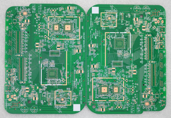
A PCB assembly line is a highly coordinated manufacturing system designed to turn bare printed circuit boards (PCBs) into fully functional electronic assemblies. Each stage in the line adds components, applies solder, and ensures electrical connections are precise and reliable. In simple terms, it’s the process that transforms a blank board into the “brain” of an electronic device.
It’s important to distinguish PCB fabrication from PCB assembly.
PCB fabrication is the process of creating the physical board itself — etching copper layers, drilling vias, and laminating materials to form the substrate.
PCB assembly, on the other hand, involves mounting and soldering electronic components onto that fabricated board to make it operational.
In the electronics supply chain, the assembly line plays a crucial role in bridging design and delivery. Prototypes are first produced to validate functionality, and once approved, the same assembly line can be scaled for mass production. This ensures consistent quality, faster time-to-market, and cost efficiency for products ranging from consumer gadgets to industrial control systems.
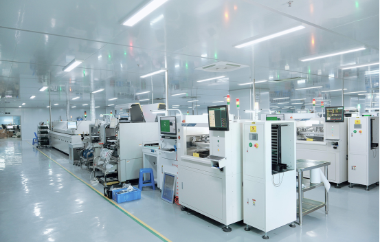
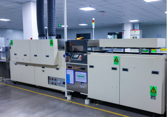
Core Components of a PCB Assembly Line
A modern PCB assembly line is built around precision automation and quality control. The main equipment typically includes:
Solder Paste Printer – Applies solder paste onto the PCB pads using a stencil, preparing the board for component placement.
Pick-and-Place Machine – Automatically picks tiny electronic components (like resistors, capacitors, and ICs) and places them onto the board with micron-level accuracy.
Reflow Oven – Heats the assembled board through a controlled temperature profile to melt the solder and create permanent joints.
Inspection Systems – Include AOI (Automated Optical Inspection) and X-ray inspection to detect soldering defects, misaligned components, or hidden connection issues.
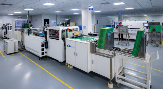
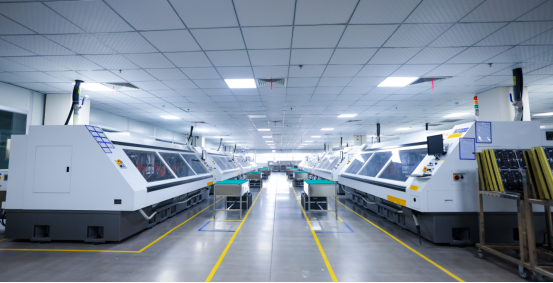
Conveyor and Handling Equipment – Move PCBs smoothly between stages, maintaining production speed and precision.
Example: In a mid-volume manufacturing plant, a typical SMT (Surface Mount Technology) assembly line might begin with a solder paste printer, followed by two high-speed pick-and-place machines, a reflow oven, and an AOI station at the end. This streamlined setup allows continuous operation — placing thousands of components per hour while maintaining strict quality control.
In essence, every element of a PCB assembly line is designed for efficiency, accuracy, and repeatability, ensuring that each circuit board leaving the line meets the exact specifications required for modern electronic products.
Step-by-Step PCB Assembly Process
The PCB assembly process is a carefully coordinated sequence of steps that ensures every electronic component is accurately mounted and soldered onto the printed circuit board. Each stage builds upon the previous one, combining precision, automation, and quality control to create reliable electronic assemblies.
Step 1 — Solder Paste Printing
The first step in the PCB assembly line is solder paste printing. Its purpose is to apply a thin layer of solder paste onto the designated pads of the PCB, where components will later be mounted. The paste, a mixture of tiny solder particles and flux, acts as both an adhesive and an electrical connector once heated.
The key equipment for this process includes a solder paste printer and a stainless-steel stencil. The printer aligns the stencil over the board and spreads the paste evenly across the surface, ensuring each pad receives the right amount.
Common issues include misalignment, which can lead to misplaced components, and insufficient or excess solder paste, which may cause weak joints or solder bridges.
Example: Modern assembly lines use automated stencil alignment systems with optical sensors to correct positioning in real time, improving yield and consistency.
Step 2 — Component Placement
Next comes component placement, where electronic parts are positioned on the PCB. This step is typically performed using SMT pick-and-place machines, which use robotic arms and vision systems to pick components from reels and place them precisely on the solder-pasted pads.
For prototypes or small batches, components may be placed manually under a microscope. However, for volume production, automated machines dominate — capable of placing thousands of parts per hour with sub-millimeter accuracy.
Example: A high-speed pick-and-place system can mount tiny 0402 resistors and complex ICs in seconds, ensuring accuracy even at high throughput.
Step 3 — Reflow Soldering
Once all components are placed, the board moves to the reflow soldering stage. Here, controlled heat is applied to melt the solder paste and create strong, permanent electrical joints.
The process follows four distinct temperature stages:
1. Preheat – Gradually raises the board’s temperature to prevent thermal shock.
2. Soak – Evens out the temperature across all components.
3. Reflow – The solder paste melts, forming reliable solder joints.
4. Cooling – Solidifies the joints for mechanical strength.
Example: In convection reflow ovens, hot air circulates to heat the PCB uniformly, while vapor-phase ovens use a controlled vapor medium for even better thermal transfer in sensitive assemblies.
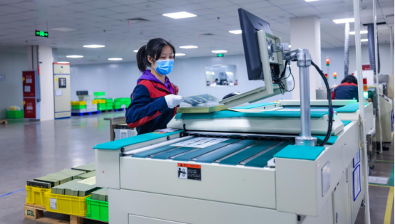
Step 4 — Inspection and Quality Control
After soldering, every PCB undergoes inspection and quality control to identify defects before they progress downstream. The most common methods include:
AOI (Automated Optical Inspection) – Uses high-resolution cameras to detect misaligned or missing components.
X-ray Inspection – Reveals hidden solder joints under BGAs and other dense packages.
Manual Visual Checks – Performed for small runs or detailed verification.
Early detection of issues such as solder bridges, cold joints, or missing components prevents costly rework later in production.
Example: AOI systems use AI-driven algorithms to automatically flag deviations from reference images, reducing false positives and increasing inspection speed.
Step 5 — Through-Hole Component Insertion (if applicable)
While SMT dominates modern electronics, some designs still require Through-Hole Technology (THT) — where components with wire leads are inserted into drilled holes in the PCB. This technique is often used for connectors, large capacitors, or high-power parts needing extra mechanical strength.
Insertion can be manual for small batches or automated using insertion machines in high-volume production. After insertion, components are soldered using wave soldering (where molten solder flows under the board) or selective soldering (targeted application for specific areas).
Step 6 — Functional Testing
Before shipment, each assembled PCB is tested to verify electrical performance. The two most common methods are:
ICT (In-Circuit Testing) – Checks individual components and connections for shorts or opens.
FCT (Functional Circuit Testing) – Simulates real-world operating conditions to confirm the board works as intended.
Example: Functional test fixtures connect to the PCB through test points, measuring voltage, current, and signal behavior to ensure the product meets design specifications.
Step 7 — Final Assembly and Packaging
The final stage involves post-testing procedures that prepare the PCB for delivery. This includes cleaning (to remove flux residues), conformal coating (for moisture or dust protection), labeling, and packaging for shipment.
Manufacturers also maintain traceability systems using barcodes or lot tracking to record production data for each batch. This ensures accountability, supports quality audits, and simplifies after-sales service.
Each of these steps — from solder paste printing to final packaging — forms part of a continuous, data-driven workflow that defines a modern PCB assembly line. Together, they ensure every circuit board meets the performance, reliability, and consistency demanded in today’s electronics manufacturing industry.
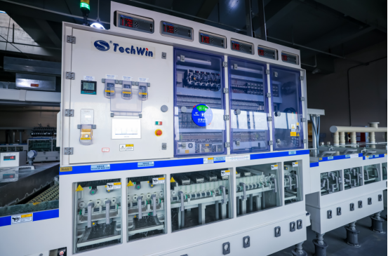
Key Equipment Used in a PCB Assembly Line
A PCB assembly line relies on a series of precision-driven machines that work together to ensure speed, accuracy, and consistency. Each piece of equipment plays a unique role — from applying solder paste to inspecting finished boards — making the entire process efficient and reliable.
Solder Paste Printer
The solder paste printer is the first and one of the most critical machines in the PCB assembly process. It applies a thin layer of solder paste onto the copper pads of the PCB through a metal stencil, creating the foundation for all subsequent steps.
High precision is essential — even a slight misalignment can cause solder bridging or open circuits later in production. Most modern printers use automatic vision alignment systems to detect fiducial marks on the PCB and perfectly align the stencil before printing.
Regular maintenance, such as cleaning the stencil and calibrating the squeegee pressure, is vital to maintain consistent print quality and prevent defects.
Example: In a high-volume SMT line, an automatic printer with closed-loop feedback control can adjust paste pressure and alignment in real time, improving yield and reducing operator intervention.
Pick-and-Place Machine
The pick-and-place machine is the workhorse of the PCB assembly line. It automatically picks tiny electronic components from reels or trays and places them onto the solder-pasted PCB pads with extreme speed and precision.
Performance is often measured in CPH (components per hour) — high-speed models can place over 100,000 components per hour, depending on board complexity.
There are two main types of pick-and-place systems:
Chip Shooters: Optimized for speed, these machines rapidly place small, simple components such as resistors and capacitors.
Flexible Placement Machines: Designed for accuracy and versatility, they handle larger or complex parts like ICs, BGAs, and connectors.
A well-balanced SMT line often combines both types to maximize throughput and placement accuracy.
Reflow Oven
Once components are placed, the board enters the reflow oven, where controlled heat melts the solder paste and creates permanent electrical and mechanical joints. The process is governed by a temperature profile — a time-based curve that defines the ideal heating and cooling cycle for a specific solder type and component layout.
A standard reflow profile includes four stages: preheat, soak, reflow, and cooling. Each stage must be carefully calibrated to prevent solder defects such as voids or cold joints.
Different oven technologies offer distinct advantages:
Convection Ovens: Use hot air for even heating, suitable for most applications.
Infrared Ovens: Provide faster heating but can cause uneven temperatures if not controlled.
Vapor Phase Ovens: Deliver the most uniform heat transfer, ideal for temperature-sensitive or high-density boards.
Optimization often involves adjusting belt speed and zone temperatures based on board size and component mix to ensure consistent solder quality.
AOI and X-Ray Inspection Systems
Automated Optical Inspection (AOI) and X-Ray inspection systems are the quality guardians of the PCB assembly line. Their main role is to detect defects early, ensuring that only flawless boards proceed to the next stage.
AOI Systems use high-resolution cameras and image recognition software to identify missing, misaligned, or incorrect components, as well as soldering issues.
X-Ray Systems are used for hidden solder joints, such as those under BGAs or QFNs, where optical inspection isn’t possible.
Modern systems increasingly leverage AI-driven inspection algorithms that can learn from previous defect data, improving accuracy over time while reducing false rejections.
Example: In a smart manufacturing environment, AI-enhanced AOI systems automatically flag patterns of recurring defects, enabling real-time process adjustments and predictive maintenance — a key feature of Industry 4.0-ready assembly lines.
In essence, the efficiency and quality of a PCB assembly line depend heavily on how these machines operate together. A precisely tuned combination of printing, placement, soldering, and inspection equipment ensures high yield, minimal downtime, and consistent product performance across every production run.
SMT vs. THT Assembly Lines — What’s the Difference?
In electronics manufacturing, SMT (Surface Mount Technology) and THT (Through-Hole Technology) represent two distinct methods of assembling components onto a printed circuit board. Each has unique advantages, applications, and equipment requirements, and understanding the difference helps engineers and procurement teams choose the right process for their products.
Surface Mount Technology (SMT) Overview
Surface Mount Technology (SMT) is the most widely used assembly method in modern electronics production. In SMT, components are mounted directly onto the surface of the PCB rather than inserted into drilled holes. These components, known as Surface Mount Devices (SMDs), are typically smaller and lighter than their through-hole counterparts, allowing for high-density circuit designs and compact product layouts.
SMT assembly lines are known for their high-speed automation and precision placement. Machines such as pick-and-place systems and reflow ovens can handle thousands of components per hour, making SMT ideal for mass production. Because of its efficiency and scalability, SMT is used in most consumer electronics, such as smartphones, laptops, and communication equipment.
Key advantage: SMT enables faster assembly, lower production costs, and more compact, multilayer PCB designs — essential for today’s miniaturized electronics.
Through-Hole Technology (THT) Overview
Through-Hole Technology (THT) is a more traditional assembly method where component leads are inserted through pre-drilled holes in the PCB and soldered to pads on the opposite side. This creates a stronger mechanical bond, making THT ideal for components that must withstand physical stress, high current, or heat.
THT is commonly used for power components, connectors, transformers, and large capacitors — parts that require stability and durability beyond what surface-mounted devices can offer.
While THT assembly is generally slower and more labor-intensive than SMT, it remains indispensable in applications like industrial controls, automotive electronics, and aerospace systems where reliability and strength are critical.
Key advantage: THT offers superior mechanical integrity, making it the preferred choice for high-stress or high-power applications.
Hybrid Assembly Lines
Many modern electronic products require both SMT and THT technologies, resulting in hybrid assembly lines that combine the advantages of each. In these setups, SMT components are typically mounted and reflow-soldered first, followed by manual or automated through-hole insertion and wave or selective soldering for larger components.
Example: A power supply unit (PSU) often uses SMT for small ICs, resistors, and capacitors on the main board, while employing THT for bulky inductors, transformers, or connectors that need robust mechanical support.
Hybrid assembly lines are designed for flexibility and versatility, allowing manufacturers to build complex, mixed-technology boards efficiently. This combination ensures both miniaturization and structural strength — essential in industries where performance and durability must coexist.
SMT excels in speed, automation, and compact design, while THT provides unmatched mechanical stability for demanding environments. Many advanced electronics today depend on hybrid assembly lines, where both technologies work together to achieve optimal performance, cost efficiency, and product reliability.
Common Challenges in PCB Assembly Lines
Operating a PCB assembly line efficiently requires careful attention to processes, equipment, and quality control. Despite automation, manufacturers often face recurring challenges that can affect yield, reliability, and production speed. Understanding these challenges and their solutions is essential for maintaining consistent output.
Process-Related Issues
One of the most common challenges in PCB assembly is process-related defects, such as solder bridging, tombstoning, and component misalignment.
Solder bridging occurs when excess solder connects two adjacent pads, creating a short circuit.
Tombstoning happens when one end of a small component lifts from the pad during reflow, resembling a tombstone.
Component misalignment arises when components are not precisely positioned on solder pads.
Root causes include incorrect solder paste application, improper reflow profiles, and inaccurate pick-and-place placement.
Preventive measures involve maintaining proper stencil alignment, calibrating pick-and-place machines, and optimizing reflow temperature profiles. By addressing these factors, manufacturers can significantly reduce defects and improve first-pass yield.
Equipment Calibration and Maintenance
Regular calibration and maintenance of PCB assembly equipment are critical for consistent output. Machines such as pick-and-place systems, solder paste printers, and reflow ovens can drift over time, affecting placement accuracy, solder quality, and production speed.
Example: Implementing predictive maintenance schedules that monitor vibration, temperature, or alignment sensors can prevent unexpected downtime. A small SMT line, for instance, can avoid hours of production loss by automatically alerting operators when a nozzle or stencil requires adjustment.
Routine calibration ensures components are placed accurately, solder paste is applied consistently, and the overall assembly line operates at peak efficiency.
Quality Assurance and Traceability
Maintaining high-quality output requires robust quality assurance (QA) practices and traceability systems. Standards such as ISO 9001 or IPC-A-610 provide guidelines for consistent manufacturing processes and product inspection.
Modern assembly lines often use digital tracking systems to record production data for every PCB. This includes lot numbers, machine settings, inspection results, and operator actions.
Benefits of traceability include:
Quick identification of defective batches.
Easier compliance with regulatory standards.
Better root-cause analysis for continuous process improvement.
By combining standardized QA protocols with digital traceability, manufacturers can ensure consistent product reliability, reduce rework costs, and enhance customer confidence.
The main challenges in PCB assembly lines—process defects, equipment drift, and quality management—can be mitigated through proper calibration, preventive maintenance, process optimization, and robust traceability systems. Addressing these areas is key to achieving high yield, operational efficiency, and product reliability.
How Automation and AI Are Changing PCB Assembly Lines
Modern PCB assembly lines are evolving rapidly with the integration of automation and artificial intelligence (AI). These technologies enhance efficiency, reduce errors, and provide real-time insights that were previously impossible in traditional manufacturing setups.
Smart Factory Integration
Smart factory integration refers to the use of real-time monitoring, connected devices, and data analytics to optimize PCB production. Sensors on machines track performance metrics such as placement accuracy, solder temperature, and component throughput, sending data to centralized systems for analysis.
Example: An Industry 4.0-enabled PCB production system can automatically adjust conveyor speeds, reflow oven temperatures, or pick-and-place alignment based on live data, ensuring consistent quality while minimizing downtime. These systems also allow managers to predict bottlenecks and schedule maintenance proactively, improving overall productivity.
By integrating smart factory technologies, manufacturers can connect every stage of the assembly line into a digital ecosystem, enabling greater transparency, faster decision-making, and scalable production.
AI in Inspection and Process Optimization
AI-driven inspection and process optimization are transforming quality control in PCB assembly. Machine learning algorithms analyze AOI (Automated Optical Inspection) and X-ray inspection data to detect defects such as misaligned components, solder bridges, or missing parts with higher accuracy than manual inspection.
AI can also adaptively optimize the assembly process. For example, algorithms learn from past production runs to adjust solder paste application, component placement speed, or reflow profiles automatically.
Benefits include:
Higher yields: fewer defective boards reach the end of the line.
Reduced manual intervention: operators spend less time correcting errors.
Continuous improvement: the system identifies recurring issues and suggests process adjustments.
Example: An AI-powered AOI system can flag subtle soldering anomalies across thousands of boards, automatically recalibrating the pick-and-place machine or alerting technicians before defects escalate.
Automation and AI are reshaping PCB assembly lines by enabling smart factory integration, real-time monitoring, and intelligent process optimization. These advancements not only improve product quality and consistency but also reduce operational costs, accelerate production, and prepare manufacturers for the demands of modern electronics markets.
Conclusion
The PCB assembly process is a carefully orchestrated sequence that transforms bare circuit boards into fully functional electronic products. From solder paste printing to component placement, reflow soldering, inspection, and final testing, each step ensures that boards meet strict performance and reliability standards. Efficiency, precision, and quality control are critical at every stage, as even minor defects can impact product functionality and customer satisfaction.
Modern assembly lines increasingly rely on automation, AI, and smart factory integration to maintain high yields, reduce errors, and optimize production workflows. By combining advanced equipment with robust quality assurance and traceability systems, manufacturers can deliver consistent, high-performance electronic assemblies.
For businesses looking to leverage cutting-edge technology, PCBMASTER’s high-performance assembly solutions provide reliable, scalable, and efficient production services, ensuring your products meet the demands of today’s competitive electronics market.
FAQs
What is the difference between PCB manufacturing and PCB assembly?
PCB manufacturing, or fabrication, creates the bare circuit board — etching copper layers, drilling holes, and applying solder masks. PCB assembly, on the other hand, mounts and solders electronic components onto the board, turning it into a working electronic device. Simply put: fabrication makes the board; assembly makes it functional.
How long does it take to complete a PCB assembly line run?
The time depends on board complexity and production volume. A small prototype may take a few hours, while high-volume automated lines can process thousands of boards in a single shift. Factors like solder paste printing, pick-and-place speed, reflow soldering, and inspection all affect the total production time.
What types of solder are used in PCB assembly?
Lead-free solder: Typically Tin-Silver-Copper (SnAgCu), used for RoHS-compliant products.
Tin-Lead solder: Older standard, sometimes used in specialized or legacy applications.
Specialty solders: Low-temperature or high-reliability alloys for sensitive electronics.
The type of solder influences reflow temperature and the durability of solder joints.
How does AOI inspection improve PCB quality?
Automated Optical Inspection (AOI) uses cameras and software to detect defects like misaligned components, missing parts, or soldering errors. It improves quality by:
Catching defects early to avoid costly rework.
Reducing human error compared to manual inspection.
Increasing first-pass yield for more consistent results.
AI-powered AOI systems can even learn from past defects to detect issues more accurately over time.
What’s the best way to optimize a PCB assembly line for small-batch production?
For small-batch PCB production, it’s best to use flexible, smaller-scale machines instead of full high-speed lines, as they allow precise control without the complexity of large-volume equipment. A modular workflow should be designed so that soldering, component placement, and inspection stages can easily scale up or down based on production needs. To save time and reduce errors, manufacturers can enable quick changeovers by pre-programming multiple board layouts into the machines. Additionally, real-time process monitoring is essential for detecting defects early, ensuring that each batch maintains high quality and consistency.
Example: For prototypes, combining automated SMT placement with manual THT insertion allows fast, accurate production without needing a full high-volume line.