


Aluminum-Based Superconductors A Low-Temperature Revolution in the PCB Industry Disruptive Breakthroughs from Principle to Application
Introduction
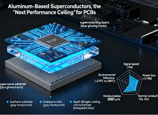
In PCB design, the choice of conductor material has always been a core challenge for engineers. While copper offers excellent conductivity, its loss issues in high-frequency, high-power scenarios have been persistently difficult to solve. The emergence of aluminum-based superconductors is bringing about a “performance revolution at low temperatures” to the PCB industry.
Imagine this: PCBs in medical equipment with signal transmission losses reduced by 90% at ultra-low temperatures; power PCBs in new energy vehicles with conduction resistance approaching zero,Resolve heat generation issues; PCBs in quantum computers achieving zero-resistance signal interconnection, boosting computational efficiency tenfold… These seemingly sci-fi scenarios are gradually becoming reality as aluminum-based superconductor technology matures.
This article uses accessible language to break down the application logic of aluminum-based superconductors in the PCB field: what they are, why they are more suitable for PCBs than traditional materials, what practical problems they can currently solve, and what changes they will bring in the future. Whether you are a PCB engineer, electronics manufacturer, or tech enthusiast, you can find key information about the integration of aluminum-based superconductors and PCBs here. Achieving the integration of aluminum-based superconductors into PCBs is a key goal in advancing PCB technology.
Shattering Perceptions - Aluminum-Based Superconductors Are Not "Future Tech," But a Practical Solution Being Implemented
When people think of superconductors, many associate them with “extreme lows of -270°C,” “expensive liquid nitrogen maintenance,” and “lab-only use.” The unique aspect of aluminum-based superconductors is that they are breaking through these limitations to become a practical, deployable technology in the PCB field. Recent advances demonstrate the practical viability of aluminum-based superconductors in PCB applications.
What are Aluminum-Based Superconductors?
Simply put, aluminum-based superconductors are materials that use aluminum or aluminum alloys as the base material, processed through special techniques (like doping, low-temperature treatment) to enter a superconducting state at specific temperatures. This “superconducting state” means electrical resistance suddenly disappears, allowing current to pass through without any loss, while also exhibiting perfect diamagnetism (the Meissner effect).
Compared to the more familiar copper-based or niobium-titanium superconductors, aluminum-based superconductors have three core advantages:
·Cost Advantage: Aluminum’s crustal abundance is over 200 times that of copper, with raw material costs only 1/5 of copper’s, making it more suitable for large-scale applications.
·Lightweight: Aluminum’s density is 2.7 g/cm³, only 1/3 that of copper, significantly reducing PCB weight (crucial for aerospace, automotive electronics, etc.).
·Process Compatibility: Aluminum’s processing temperature (melting point 660°C) is lower than copper’s (1083°C), making it easier to integrate with existing PCB manufacturing processes.
Currently, there are two main types of practical aluminum-based superconductors:
·Pure Aluminum Superconductors: Aluminum with purity above 99.999%, entering a superconducting state at 1.17K (approx. -272°C). While requiring extremely low temperatures, their simple structure is an advantage.
·Aluminum Alloy Superconductors: By doping with elements like gallium or germanium, the critical temperature (T-C) is raised, with values reaching 2-3K, while mechanical strength is 30% higher than pure aluminum, making them more suitable for PCB traces. The values of both critical temperature (T-C) and mechanical strength are improved in aluminum alloy superconductors.
Why Do PCBs Need Superconductors?
Traditional PCB copper traces have two “inherent flaws” that are increasingly failing to meet demands in high-end fields. The adoption of aluminum-based superconductors enables enhanced superconductivity in PCB applications, leading to superior performance.
Resistive Loss is Unavoidable
Copper's resistivity is about 1.7×10⁻⁸ Ω·m. While excellent among metals, losses increase dramatically in high-frequency, high-current scenarios. For example:
·In 5G base station PCBs, high-frequency signals in copper traces suffer 3x increased losses compared to low frequencies due to the "skin effect" (current concentrating on the conductor surface).
·In new energy vehicle power PCBs, power dissipation can reach 5W per square centimeter cross-sectional area for high currents passing through copper traces, necessitating complex cooling structures.
Superconductors have zero resistance, theoretically eliminating these losses. Experimental data shows: under the same current, the power dissipation of aluminum-based superconductor PCBs is only 0.1% of that of copper trace PCBs.
Electromagnetic Interference (EMI) is Difficult to Control
Current flowing through copper traces generates magnetic fields, causing "crosstalk" between adjacent traces and affecting signal integrity. In high-density PCBs (like server motherboards with over 100 traces per square centimeter), this interference increases data transmission error rates.
The perfect diamagnetism (Meissner Effect) of superconductors "repels" external magnetic fields and does not generate fields itself, solving EMI problems at the root. Tests show: signal crosstalk in aluminum-based superconductor PCBs is reduced by 99% compared to copper trace PCBs.
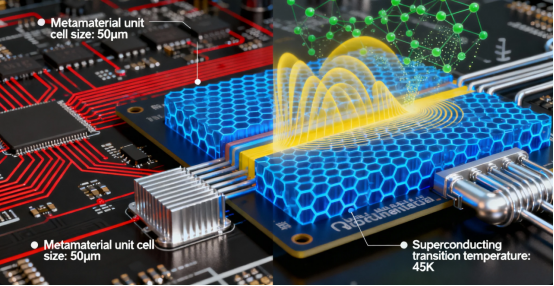
Metamaterial Properties: Unlocking New Functionalities in Superconducting PCBs
One of the most important goals in condensed matter physics and advanced PCB engineering is the design of materials with enhanced superconducting properties. Recent research has brought aluminum-based hyperbolic metamaterials to the forefront, offering a striking example of how the metamaterial approach can deterministically enhance superconductivity and unlock new functionalities in superconducting PCBs.
Unlike traditional copper substrates, which have long been favored for their high conductivity and suitability for wire bonding, aluminum-based hyperbolic metamaterials and core-shell metamaterial superconductors have demonstrated superior transport and magnetic properties. Recent experiments have shown that by carefully engineering the thickness, density, and composition of these materials, engineers can reliably predict and achieve desired properties—most notably, a critical temperature (Tc) enhancement of up to three times that of pure aluminum. This deterministic enhancement is a game-changer for applications where higher Tc and superior magnetic properties are essential.
A key challenge in the development of aluminum-based superconductors is the formation of aluminum oxide, which can increase resistance and degrade superconducting properties. To address this, researchers have turned to oxidation-resistant materials and advanced fabrication techniques such as atomic layer etching and deposition. These methods allow for precise control over the material’s structure, minimizing unwanted oxidation and ensuring that the superconducting properties are preserved or even enhanced.
The combination of aluminum with other metals, such as gold, has also proven effective in achieving similar Tc enhancement and superior transport characteristics. This synergy not only improves the superconducting performance but also expands the range of suitable materials for specific applications, from quantum computing to high-frequency signal transmission. The ability to fine-tune the material’s properties through the metamaterial approach means that engineers can now develop superconducting PCBs tailored for optimal performance in demanding environments.
Furthermore, the use of core-shell metamaterial superconductors has opened new avenues for wire bonding and integration with existing PCB technologies. By leveraging the unique magnetic properties compared to conventional materials, these advanced structures enable the development of superconducting devices with reduced loss, higher reliability, and greater design flexibility.
In summary, the development and application of aluminum-based hyperbolic metamaterials represent a significant leap forward in the production and design of superconducting PCBs. Through the use of advanced materials, precise fabrication techniques, and a deep understanding of condensed matter physics, engineers are now able to achieve deterministic enhancement of superconducting properties. As research continues to advance, these innovations are set to drive the next wave of breakthroughs in quantum computing, superconducting devices, and beyond—demonstrating the transformative potential of the metamaterial approach in achieving the most important goals of modern electronics.
Technological Breakthroughs - How Aluminum-Based Superconductors "Adapt" to PCB Manufacturing? Analysis of 3 Key Processes
The biggest challenge in applying superconductors to PCBs isn’t the superconductor material itself, but making it compatible with PCB manufacturing workflows. Specialized fabrication steps are performed to ensure aluminum-based superconductors are compatible with these workflows. While traditional superconductors (like Niobium-Titanium) are hard and difficult to process, aluminum-based superconductors, with their good malleability, have achieved initial integration with PCB processes.
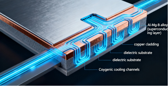
PCB-Level Processing of Superconducting Wires: Breakthrough from "Thick Wires" to "Thin Films"
For superconductors to be used in PCB traces, they must be made into “thin films” or “fine wires” just a few micrometers to tens of micrometers thick, placing extremely high demands on processing aluminum-based superconductors. The number of layers deposited and the number of process steps are critical factors in achieving the desired film thickness and precise patterning. Two mainstream methods exist:
Magnetron Sputtering:
In a vacuum environment, high-energy particles bombard an aluminum target, causing aluminum atoms to deposit on the PCB substrate (e.g., aluminum oxide ceramic, sapphire) surface, forming a 5-20μm thick aluminum-based superconducting film. Advantages:
·Excellent film uniformity, thickness deviation controllable within ±0.5μm.
·Can directly form patterned traces on insulating substrates (via masks), no subsequent etching needed.
·One lab used this method to create aluminum-based superconducting traces on a 6-inch ceramic substrate, achieving a minimum line width of 50μm, meeting most high-precision PCB needs.
Rolling-Etching Method:
First roll the aluminum-based superconductor material into 10-50μm thick foil, then process it into the desired trace pattern using etching similar to traditional PCB processes. Advantages:
·High compatibility with existing PCB etching processes, no large-scale production line modifications needed.
·Can produce thicker traces (above 50μm), suitable for high-current scenarios (e.g., power PCBs).
·Disadvantage: Slightly poorer thickness uniformity (deviation ±2μm), and the etching process might affect superconducting properties, requiring strict control of etchants (avoid chlorine-based solutions to prevent aluminum oxidation).
2. "Miniaturization" of the Low-Temperature Environment: How Can PCBs "Bring Their Own Refrigeration"?
Aluminum-based superconductors need to operate at very low temperatures (1-3K), meaning the PCB must incorporate a micro-refrigeration system. Traditional liquid nitrogen refrigeration is bulky (e.g., lab Dewar flasks) and cannot be integrated onto a PCB. Achieving ideal cooling conditions is crucial for maintaining the superconducting state in aluminum-based superconductor PCBs. Two new technologies are changing this:
Miniature Stirling Coolers:
These devices cool via gas expansion, can be shrunk to 5cm×3cm×2cm (matchbox size), can lower local temperatures below 1K, with power consumption around 10W. When integrating with aluminum-based superconductor PCBs:
·The cooler's cold head directly contacts the superconducting trace area, transferring cold via thermal grease (special type remaining elastic at low temps).
·PCB substrate uses high thermal conductivity materials (e.g., aluminum nitride ceramic, thermal conductivity 200 W/(m·K)) to ensure uniform temperature in the superconducting area.
·This solution is already used in miniaturized superconductor PCBs for medical devices, like MRI signal receiver PCBs, reducing volume by 60% compared to traditional solutions.
Adiabatic Demagnetization Refrigeration:
Utilizes the principle where certain paramagnetic materials (like Gadolinium Gallium Garnet) magnetize and release heat when a magnetic field is applied, and absorb heat when removed, achieving cooling without moving parts. Can be even smaller (3cm×2cm×1cm) and vibration-free (crucial for precision instruments).
·Disadvantage: Longer cooling cycles (one cycle lasts 2-4 hours), suitable for intermittent operation PCB scenarios (e.g., detection equipment PCBs on satellites, can initiate cooling periodically during orbit).
3. Insulator-Superconductor Compatibility: Avoiding "Killing" the Superconducting Properties
If the insulating layers in a PCB (like solder mask, substrate) react chemically with the aluminum-based superconductor, or have poor thermal conductivity, it can degrade or even destroy superconductivity. Exposure to air during processing can lead to the formation of a passive aluminum oxide layer on aluminum surfaces, which complicates subsequent soldering and surface treatment steps. Therefore, insulating material selection has three special requirements:
Chemical Stability:
Insulating materials must not contain components that react with aluminum (e.g., halogens, heavy metal ions). Experiments show: traditional PCB FR-4 substrate contains trace chlorine, which reacts with aluminum-based superconductors at low temps forming aluminum chloride, reducing the critical temperature by 20%. Thus, aluminum-based superconductor PCBs need "halogen-free ceramic substrates" (e.g., aluminum oxide, silicon nitride).
Low-Temperature Compatibility:
Common organic insulating materials (like epoxy resin) become brittle and crack at low temperatures, while ceramics or modified polyimide remain flexible at 1K, suitable as insulating layers between superconductor and substrate.
Thermal Conductivity Matching:
The insulator's thermal conductivity cannot be too low, otherwise it hinders heat transfer from the cooling system. For example: Aluminum nitride ceramic's thermal conductivity is over 50 times that of FR-4, ensuring temperature uniformity (temperature difference ≤0.1K) in the superconducting trace area.
Application Scenarios: Aluminum-Based Superconductor PCBs Are Already "Bearing Fruit" in These 3 Fields
Although aluminum-based superconductor PCBs are still in the early stages of industrialization, they have achieved commercial application in fields with extremely high performance demands and lower cost sensitivity, demonstrating advantages unmatched by traditional PCBs. Aluminum-based superconductor PCBs are capable of meeting the stringent requirements of advanced applications in medical, quantum computing, and aerospace fields.
1. Medical Equipment: Making MRI Signals Clearer, Devices More Compact
The core of an MRI device is the "receiver coil PCB," responsible for capturing magnetic resonance signals from body tissues. Signal strength directly determines image clarity. Traditional copper trace PCBs have two problems:
·Significant signal loss during transmission leads to high imaging noise (especially reducing ability to identify tiny lesions like early tumors).
·To reduce loss, coils must be large (diameter over 1 meter), resulting in bulky equipment and poor patient experience.
A medical device company using aluminum-based superconductor PCBs for MRI receiver coils achieved two breakthroughs:
·Signal transmission loss reduced by 95%, image clarity improved 3-fold, able to identify lesions as small as 0.5mm in diameter.
·Coil diameter reduced to 30cm, device volume decreased by 50%, significantly reducing patient claustrophobia during scans.
·This superconductor coil is now used in high-end brain MRI devices. Although cost is 3 times higher than traditional copper coils, the improved diagnostic accuracy has led to rapid adoption in tertiary hospitals.
2. Quantum Computing: Solving the Key Bottleneck of "Qubit Interconnection"
The PCB in quantum computers (called the “quantum interconnect PCB”) needs to connect tens to hundreds of qubits, enabling signal transmission between them. Two flaws of traditional copper trace PCBs become “showstoppers” for quantum computing:
·Resistance in copper traces causes qubit signal attenuation, shortening entanglement time between qubits (from tens of microseconds to a few microseconds).
·Magnetic fields generated by copper traces interfere with qubit states, increasing computational error rates.
IBM uses aluminum-based superconductor PCBs as the quantum interconnect layer in its “Eagle” quantum computer, bringing changes:
·Qubit signals transmit through superconducting traces with almost no attenuation, extending qubit entanglement time beyond 100 microseconds.
·Perfect diamagnetism avoids magnetic interference, reducing computational error rates by 60%.
·This superconductor PCB achieves a trace precision of 10μm, enabling interconnection of 200 qubits within a 1cm² area, making scaling quantum computers possible.
Several university research groups have also contributed to the development and testing of these advanced quantum interconnect PCBs, often through collaborations and research grants focused on quantum computing technologies.
3. Aerospace: Lightweight + Low Loss, Enhancing Equipment Reliability
Satellite and spacecraft electronic systems have two stringent requirements for PCBs: lightweight (every 1kg saved reduces launch cost by ~$10,000) and low power
consumption (rely on solar power). Traditional copper trace PCBs have limitations here:
·Copper’s high density leads to heavy PCB weight (total PCB weight of a communication satellite can exceed 50kg).
·Losses during high-power transmission (e.g., ~90% conversion efficiency for power PCBs) waste precious electrical power.
The European Space Agency (ESA) used aluminum-based superconductor power PCBs on its “Metop” satellite, with notable results:
·For the same current-carrying capacity, the superconductor PCB is 60% lighter than the copper PCB, reducing satellite weight by 15kg, saving $150,000 in launch costs.
·Power transmission efficiency increased from 90% to 99.9%, providing an extra 2kWh of energy daily, extending satellite operation time.
·Additionally, the radiation resistance of aluminum-based superconductors (superconducting property decay under space radiation is 50% slower than copper) also improves long-term PCB reliability, increasing satellite design life from 5 to 7 years.
The unique challenges presented by the harsh aerospace environment have driven further innovation in superconductor PCB design.
Challenges and Future: How Far Are Aluminum-Based Superconductor PCBs from Widespread Application?
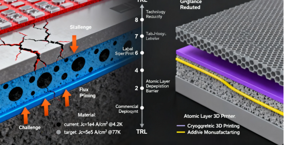
Despite breakthroughs in specific fields, aluminum-based superconductor PCBs need to solve three core challenges before becoming as ubiquitous as traditional copper PCBs. Ongoing research is focused on design materials with tailored superconducting properties, aiming to engineer next-generation PCBs with enhanced performance and reliability.
1. Cooling Cost: Leap from "Expensive" to "Affordable"
Currently, micro-cooling system costs account for 70% of the total cost of aluminum-based superconductor PCBs (e.g., a Stirling cooler costs about $2000), putting it out of reach for most consumer electronics. Solutions lie in two directions:
·Material Improvement: Develop "high-temperature aluminum-based superconductors," raising the critical temperature from 1-3K to above 20K (closer to liquid nitrogen temperature, 77K), allowing cheaper liquid nitrogen cooling (costing 1/10 of Stirling coolers).
·Cooling Efficiency Improvement: New magnetic refrigeration technology (using the magnetocaloric effect) is under testing, potentially reducing power consumption by 50% and shrinking volume below 2cm³, expected to be commercialized before 2030.
2. Process Compatibility: Integration with Existing PCB Production Lines
The current processing yield for aluminum-based superconductor PCBs is about 60% (compared to 95% for traditional copper PCBs), mainly because superconducting materials are more sensitive to the processing environment (e.g., humidity, impurities). Improvements include:
·Cleanroom Upgrade: Elevate PCB manufacturing cleanliness from Class 1000 (≤1000 particles of 0.5μm or larger per cubic foot) to Class 100, reducing impurity contamination.
·Etching Process Optimization: Adopt "ion beam etching" instead of chemical etching, avoiding chemical reactions affecting superconductivity, potentially increasing yield to over 85%.
3. Design Standards: Establishing Common Industry Specifications
Currently, there are no unified standards for designing aluminum-based superconductor PCBs (e.g., trace spacing, thermal design, reliability test methods), leading to compatibility issues between products from different manufacturers. There has been a growing request from manufacturers and designers for unified design standards in this field. The industry is promoting two efforts:
·International Standard Development: The IEC has established a “Superconducting PCB Working Group,” planning to release the first version of design specifications by 2025.
·Simulation Tool Development: Companies like ANSYS and Cadence are developing simulation software specifically for superconductor PCBs, modeling signal transmission and thermal distribution at low temperatures, reducing design difficulty.
Conclusion: Aluminum-Based Superconductors, the "Next Performance Ceiling" for PCBs
From laboratories to medical equipment, quantum computing, and aerospace, aluminum-based superconductors are steadily making their way into practical PCB application scenarios. They might not completely replace copper (at least not in room-temperature, low-cost scenarios), but they will undoubtedly become an indispensable key material in fields demanding ultimate performance.
For PCB engineers, now is the perfect time to understand and follow this technology. In the next 5-10 years, as cooling costs drop and processes mature, aluminum-based superconductor PCBs could appear in more areas: from high-frequency PCBs in 5G base stations to power control boards in new energy vehicles, from interconnect PCBs in supercomputers to low-power sensor boards in wearable devices.
What aluminum-based superconductors bring to the PCB industry is not just a material change, but an innovation in design thinking. When resistance is no longer a limit and electromagnetic interference is no longer a problem, the functions PCBs can achieve will break through existing boundaries of imagination. This "low-temperature revolution" is worth anticipating.
FAQs
Q. What are aluminum-based superconductors?
A. Materials that use aluminum or aluminum alloys as the base, processed through doping, low-temperature treatment, and other techniques to achieve zero electrical resistance and perfect diamagnetism (Meissner effect) at specific low temperatures.
Q. What is their typical superconducting critical temperature (Tc)?
A. Pure aluminum superconductors: approximately 1.17-1.2K (-272°C). For aluminum alloys doped with elements like gallium or germanium, Tc can be raised to 2-3K.
Q. What are the core advantages compared to copper-based and niobium-titanium superconductors?
A. Three standout advantages: lower cost (raw material price is about 1/5 that of copper), lighter weight (density is only 1/3 that of copper), and better process compatibility (lower melting point, easier integration into PCB workflows).
Q. In which fields are they currently primarily applied?
A. Focused on high-end scenarios: quantum computing (quantum bit interconnect PCBs), medical equipment (MRI receiver coils), aerospace (lightweight, low-loss power PCBs).
Q. Why are they suited for quantum computing requirements?
A. Zero resistance prevents quantum signal attenuation, extending bit entanglement time; perfect diamagnetism eliminates magnetic interference, reducing computational error rates. For example, IBM's "Eagle" quantum computer already employs them.
Q. What is the biggest technical challenge in their application?
A. High cost of maintaining low temperatures (refrigeration systems account for ~70% of total cost), insufficient compatibility with existing PCB production lines (~60% yield), and lack of unified design standards.
Q. How to break through the low-temperature refrigeration bottleneck?
A. Two main approaches: First, develop high-temperature aluminum-based superconductors to raise Tc above 20K for compatibility with cheaper liquid nitrogen cooling. Second, develop miniature magnetic refrigeration technology to reduce power consumption and size.
Q. Can they replace traditional copper-based PCBs in the future?
A. Unlikely to fully replace them in the short term; copper remains suitable for room-temperature, low-cost scenarios. However, they will become core materials in fields demanding high frequency, high power, and ultimate performance (e.g., 5G base stations, new energy vehicles).
Q. How do material defects affect their performance?
A. Defects such as surface oxygen vacancies and grain boundaries can cause flux noise and reduce the quantum coherence time (T1). Techniques like argon ion beam polishing are required to lower the defect density.
Author: Jack Wang

