


High-Precision PCB Manufacturing: Key Techniques & Materials
You wouldn't trust just any blueprint to build a skyscraper. The same logic applies to High-Precision PCBs, where every layer, trace, and material choice must align with precise engineering demands. It's not just about making something work; it's about making it work flawlessly under pressure—whether it's withstanding the extremes of aerospace or ensuring the ultra-reliability required in medical implants. As technology pushes the boundaries of what’s possible, these boards are the silent enablers of progress, where every minute detail can make or break the final outcome.
The Importance of High-Precision PCB Manufacturing
Defining High-Precision PCBs
High-Precision printed circuit boards (PCBs) are integral to the modern electronic landscape, offering the foundation for everything from advanced medical devices to cutting-edge telecommunications. Unlike standard PCBs, High-Precision boards are designed to handle intricate, high-performance requirements.
Key characteristics of High-Precision PCBs include:
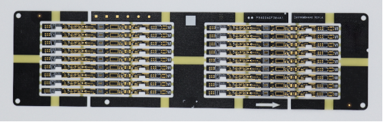
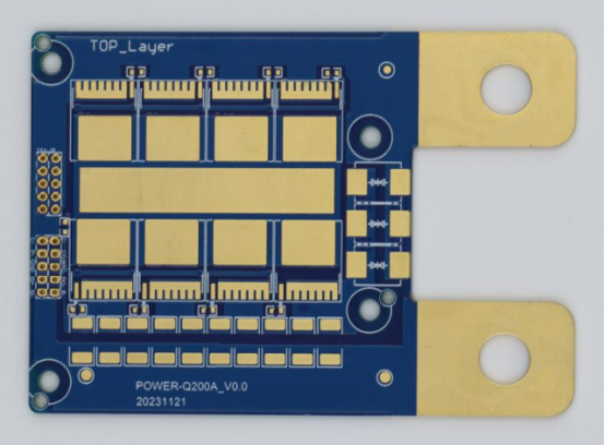
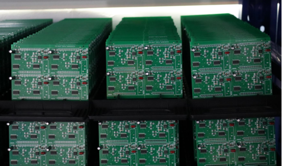
Multi-Layer Structures: These PCBs typically feature 10+ layers, sometimes exceeding 20 or even 30, to support complex circuitry and compact designs. The multiple layers allow for greater circuit density and more functionality in a smaller space.
Fine-Pitch Components: Fine-pitch components with very small distances between pads or traces (as small as 0.3mm) are used to enable higher performance without compromising size.
Controlled Impedance: Impedance control is essential for high-speed signals to travel with minimal distortion. Proper impedance matching ensures signal integrity, crucial for applications like RF (radio frequency) and high-speed digital communication.
These features are vital in applications requiring precision, where failure is not an option. For example, aerospace PCBs must endure extreme environmental conditions, while medical PCBs must operate reliably in life-critical systems.
Why Techniques and Materials Matter
The performance and reliability of High-Precision PCBs depend heavily on the manufacturing techniques and materials used. The advanced design and high-stakes environments these boards operate in demand precise, specialized production processes.
Advanced Manufacturing Techniques
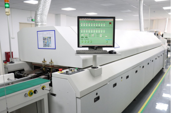
Techniques like laser drilling, microvia formation, and automated optical inspection (AOI) play a critical role in ensuring quality. Laser drilling, for example, allows manufacturers to create ultra-fine vias (as small as 50µm) that are essential for high-density interconnect (HDI) boards. These fine vias support smaller, more powerful components while maintaining signal integrity. Similarly, microvia technology helps reduce crosstalk and improves signal clarity, making it a must-have for high-speed applications like 5G and RF communications.
Material Selection
The right materials are crucial for achieving the performance characteristics demanded by complex PCBs. High-frequency applications, for instance, require materials like Rogers RO4350B or Isola FR408HR, which offer low signal loss and stable electrical properties at high frequencies. Materials must also be chosen to withstand extreme temperatures, mechanical stress, and even radiation, especially in fields like aerospace and medical devices. For instance, aerospace PCBs often use space-grade materials capable of withstanding harsh conditions like extreme heat, cold, and radiation.
Together, advanced techniques and specialized materials enable High-Precision PCBs to perform reliably in critical applications, where any failure can result in catastrophic consequences. These factors not only enhance performance but also ensure that the board can operate in diverse and challenging environments, from the harsh vacuum of space to the delicate conditions of human implants.
In summary, High-Precision PCB manufacturing is not just about producing a functional circuit board; it’s about creating a precision tool that meets rigorous standards across multiple industries. The combination of cutting-edge techniques and carefully selected materials guarantees that these boards will perform at the highest level, no matter how challenging the application.
Key Techniques in High-Precision PCB Manufacturing
Advanced Layer Stackup Design
In High-Precision PCB manufacturing, the layer stackup is a critical aspect that directly influences the performance of the circuit board. A customized stackup helps optimize signal integrity and electromagnetic compatibility (EMC), both of which are essential in high-speed and high-frequency applications.
Role of Customized Stackup in High-Speed and High-Frequency Applications
The stackup defines how layers of the PCB are arranged, including the order of signal layers, ground planes, and power planes. A well-designed stackup minimizes signal interference and ensures that high-speed signals travel without degradation. It also ensures controlled impedance, a key factor for maintaining the integrity of signals in applications like 5G communications, RF circuits, and data transmission.
Example
One common example is a 20+ layer HDI (High-Density Interconnect) board used in telecommunications or high-performance computing. In these boards, controlled impedance is crucial to prevent signal reflections and crosstalk. By customizing the stackup, manufacturers can optimize each layer for specific functions, such as improving signal integrity or minimizing power distribution noise.
Microvia and Buried Via Technology
Microvias and buried vias are essential technologies in High-Precision PCBs, especially in HDI boards that require high component density and fine pitch. These technologies allow for more compact designs, reducing the size of the PCB while enhancing signal performance.
How Microvias and Buried Vias Help Reduce Crosstalk and Enhance Signal Density
Microvias are small, laser-drilled vias that allow for high-density interconnects in multi-layer PCBs. By reducing the space between layers, microvias significantly improve signal routing, reduce crosstalk, and provide better signal integrity. Buried vias, which are internal to the PCB, further enhance the design by reducing the need for external routing, minimizing interference, and increasing overall signal density.
Case Study
A 16-layer automotive PCB is a perfect example of how microvia technology enhances performance. In this case, the PCB is designed for use in automotive electronics, where space is limited, and the components need to be tightly packed. Microvias allow the PCB to have a higher layer count while maintaining a compact footprint. The use of microvias in this 16-layer PCB helps ensure that high-speed signals, such as those used in automotive control systems, remain clear and free from noise.
Thermal Management Solutions
Thermal management is critical in High-Precision PCBs, especially in power-intensive designs where heat dissipation is a major concern. Effective thermal management ensures that components do not overheat, which can degrade performance or cause failures.
Techniques for Managing Heat in Power-Intensive Designs
Various techniques are employed to manage heat in complex PCBs:
Thermal vias: These are drilled vias that provide a path for heat to flow from high-temperature areas to heat sinks or other parts of the PCB designed for heat dissipation.
Heat sinks: These are attached to the PCB to absorb and dissipate heat away from sensitive components.
Copper planes: Large copper planes within the PCB can act as heat spreaders, helping to distribute heat more evenly across the board.
Exampl
A PCB for automotive applications with embedded resistors is tested for a wide temperature range of -40°C to 125°C to ensure it can withstand extreme environmental conditions. In this case, the PCB uses thermal vias and heat sinks to manage the heat generated by power-intensive components, such as resistors or processors. These thermal solutions help prevent damage from overheating and ensure that the automotive system continues to function reliably under harsh conditions.
Advanced techniques like layer stackup design, microvia and buried via technology, and thermal management solutions are the backbone of High-Precision PCB manufacturing. By carefully selecting and implementing these technologies, manufacturers can create PCBs that are not only compact and efficient but also capable of performing reliably in high-speed, high-frequency, and power-intensive applications. These techniques are essential for industries like telecommunications, automotive, aerospace, and medical devices, where performance and reliability are paramount.
Essential Materials for High-Precision PCBs
Advanced Substrates
The substrate is the foundational material of any PCB, providing mechanical support and electrical insulation for the conductive traces. For High-Precision PCBs, selecting the right substrate material is critical to ensure optimal performance, especially in high-speed and high-frequency applications.
Common Materials for Specific Applications
Rogers RO4350B is a popular choice for RF (radio frequency) applications due to its low loss and stable electrical properties at high frequencies. Its low dielectric constant (Dk) ensures minimal signal degradation, making it ideal for high-performance RF and microwave circuits.
Isola FR408HR is commonly used in high-temperature resistance applications. It is especially useful in automotive and aerospace PCBs where components are exposed to extreme temperatures. FR408HR maintains stability under high thermal stress, making it ideal for environments where temperature fluctuations are frequent and intense.
Choosing the Right Substrate for Performance
When selecting a substrate, performance factors like low loss, high frequency, and thermal resistance must be considered. For example, in high-frequency circuits, substrates with low dielectric loss and stable Dk, like Rogers RO4350B, are preferred to minimize signal attenuation. In contrast, high-temperature applications demand materials like Isola FR408HR that can withstand thermal cycling without compromising integrity.
Copper Foil Grades and Dielectric Control
Copper foils and dielectric materials play a crucial role in maintaining the electrical integrity and performance of High-Precision PCBs. The choice of copper foil grade and the control over dielectric thickness are key factors in ensuring that the board meets the required specifications.
Ultra-Thin Copper Foils
In high-density designs, ultra-thin copper foils (as thin as 1/8 oz) are used for fine-pitch traces. These thinner foils enable tighter spacing between traces, allowing for higher density and miniaturization of components. Thinner copper foils also contribute to better electrical performance by reducing resistance and improving current flow, which is crucial for high-speed circuits.
Dielectric Thickness Control
Dielectric material is placed between the copper layers to maintain the correct electrical impedance. For high-frequency applications, precise control over the dielectric thickness (within ±5%) is essential to maintain impedance stability. Any variation in the dielectric thickness can lead to signal reflections, causing performance issues such as signal distortion or loss. Controlling the dielectric thickness ensures that the impedance is uniform across the PCB, which is crucial for high-speed signal integrity.
Solder Mask and Surface Finishing
The solder mask and surface finishing are essential for protecting the PCB and ensuring reliable electrical connections during assembly. These materials contribute to the overall durability and performance of the PCB.
Solder Mask Application
The solder mask is a protective layer that prevents unwanted solder bridges and protects the PCB’s copper traces from corrosion. Inkjet technology is increasingly used for solder mask application due to its precision. This method allows for the deposition of ultra-thin, highly accurate solder masks, ensuring precise exposure of the pads and traces. This is especially important for fine-pitch components where traditional methods may not provide sufficient accuracy.
Surface Finishes
The surface finish is applied to the PCB to facilitate reliable soldering and ensure that the electrical connections are stable. One of the most popular finishes for high-precision boards is ENIG (Electroless Nickel Immersion Gold). ENIG provides a uniform layer of nickel and gold, which offers excellent corrosion resistance and creates a reliable surface for soldering. This finish is commonly used in high-frequency and high-reliability applications, such as medical devices and aerospace electronics, where long-term durability and stable electrical connections are crucial.
The materials used in High-Precision PCBs play a pivotal role in determining the board’s overall performance and reliability. By carefully selecting advanced substrates, using ultra-thin copper foils, controlling dielectric thickness, and applying precise solder masks and finishes, manufacturers can ensure that these PCBs perform flawlessly in demanding environments. Whether it's for RF communication, aerospace, or high-temperature applications, choosing the right materials ensures that the PCB can handle the required electrical and thermal stresses while maintaining signal integrity and reliability.
Integrating Techniques and Materials for Optimal Performance
How Materials and Techniques Work Together
In High-Precision PCB manufacturing, the relationship between materials and techniques is key to achieving optimal performance. The right material selection combined with advanced manufacturing techniques ensures that the board meets its design requirements, such as signal integrity, thermal management, and mechanical stability.
Example
In high-frequency applications, such as RF circuits or 5G communication, choosing the right material, like Rogers RO4350B, is essential due to its low dielectric constant and low loss characteristics. When this material is combined with advanced techniques, like microvia technology, the PCB's performance is enhanced. Microvias allow for high-density interconnects in a small footprint, minimizing signal interference and ensuring the integrity of high-speed signals. The fine-pitch trace routing enabled by microvias, when combined with the low loss substrate, significantly improves signal clarity and reduces crosstalk, making it perfect for applications where performance cannot be compromised.
Ensuring Synergy Between Materials and Techniques
The materials and techniques used in PCB manufacturing must complement each other to achieve the desired results. For instance, the dielectric constant (Dk) of a material, which determines how the material interacts with electrical signals, needs to align with the manufacturing technique used. In laser drilling, for example, the precise control of the laser can help create microvias with minimal thermal damage to the surrounding substrate. If the material's properties are not compatible with the drilling technique, it may result in poor-quality vias, affecting signal integrity. By carefully selecting materials and techniques that work well together, manufacturers can ensure that the PCB performs optimally in high-speed, high-frequency applications.
Quality Control Through Advanced Inspection
Once the materials are selected and the advanced techniques are applied, ensuring the quality of the final product is critical. Advanced inspection methods are employed to detect any potential defects, verify performance, and ensure that the PCB meets strict industry standards.
Automated Optical Inspection (AOI) for Trace Verification
AOI is a key quality control tool in High-Precision PCB manufacturing. This automated system uses high-resolution cameras to scan the PCB for any defects in trace routing, soldering, or layer alignment. The system can detect issues like misaligned traces, open circuits, or short circuits, ensuring that the PCB’s electrical pathways are correct and intact. AOI is crucial for identifying issues early in the production process, which helps to reduce the risk of failure in the final application.
X-Ray Imaging for Layer Alignment and Registration Checks
In multi-layer PCBs, ensuring that the layers are correctly aligned is essential for maintaining signal integrity and mechanical strength. X-ray imaging is used to inspect the alignment of internal layers that cannot be visually examined. It allows manufacturers to verify via placement, buried via quality, and layer registration with precision, ensuring that the board will function as expected. For example, it can detect layer misregistration in HDI (High-Density Interconnect) boards, which can lead to signal loss or crosstalk if not corrected.
Impedance Testing Using Time Domain Reflectometry (TDR)
Impedance control is critical for high-speed and high-frequency PCBs, where even small impedance mismatches can cause significant signal distortion. Time Domain Reflectometry (TDR) is a method used to measure and verify the controlled impedance of traces across the PCB. It sends a signal through the PCB and measures the reflected signal to identify any impedance variations. This ensures that the signal travels with minimal reflection and degradation, maintaining the signal integrity necessary for high-performance applications such as RF and 5G.
Integrating the right materials with advanced manufacturing techniques is essential for achieving optimal performance in High-Precision PCBs. The synergy between materials like low-loss substrates and techniques like microvias ensures that the PCB can meet the demands of high-speed, high-frequency, and power-intensive applications. Furthermore, advanced inspection methods like AOI, X-ray imaging, and TDR impedance testing are crucial for verifying the quality and functionality of the board, ensuring that it will perform reliably in demanding environments. These combined efforts enable manufacturers to produce PCBs that meet stringent performance and quality standards, delivering superior performance in critical applications.
Tips for Optimizing High-Precision PCB Projects
Design for Manufacturability (DFM)
Design for Manufacturability (DFM) is a critical approach in PCB design that focuses on ensuring the design can be efficiently and cost-effectively manufactured without compromising performance. Collaboration between design engineers and manufacturers early in the process can prevent costly issues during production.
Collaborating with Manufacturers to Optimize Design
Early involvement from manufacturers helps identify potential design flaws that could complicate the manufacturing process. For example, via-in-pad issues, where a via is placed directly under a component pad, can lead to difficulties in soldering and create potential for short circuits. By addressing such issues in the design phase, manufacturers can suggest alternative routing options or recommend design changes that simplify the manufacturing process, ensuring a smoother production flow.
Material Selection Considerations
Choosing the right materials is essential for ensuring a PCB performs well under its specific operating conditions. High-Precision PCBs often require materials tailored to meet thermal, electrical, and mechanical requirements, as these boards face demanding conditions in applications such as aerospace, medical devices, and automotive electronics.
How to Select Materials Based on Thermal, Electrical, and Mechanical Requirements
The material selection process involves understanding the board's intended use and environment. For example, high-frequency applications (like RF circuits) require low-loss substrates such as Rogers RO4350B to reduce signal degradation. Similarly, if the PCB is exposed to extreme temperatures, materials like Isola FR408HR, known for its high-temperature resistance, should be used. For high-power applications, materials with good thermal conductivity and mechanical strength, like ceramic-based substrates, may be required to ensure long-term reliability.
Why Material Certification and Traceability Are Critical
For high-stakes applications, such as aerospace or medical devices, material certification and traceability are essential. Certified materials meet specific industry standards for performance and safety, which are crucial in these fields. For example, ISO-certified materials ensure that they have passed rigorous quality control tests, guaranteeing their reliability. Traceability allows manufacturers to track the material's source and performance history, providing assurance that it meets the required specifications and will perform reliably over time.
Prototyping and Simulation
Prototyping and simulation are vital steps in the development process of High-Precision PCBs. These methods help test design concepts, validate performance, and make adjustments before moving to mass production, reducing the risk of costly design errors.
The Role of Rapid Prototyping in Testing Design Concepts
Rapid prototyping allows designers to quickly produce a physical model of the PCB to test its functionality and performance. This approach is particularly useful in verifying the design’s electrical characteristics, layout, and mechanical fit before committing to full-scale production. Prototypes help identify potential issues such as trace routing errors or thermal management problems that might not be apparent in the initial design phase. For example, a prototype might reveal that certain components are too close to heat-sensitive areas, requiring adjustments to the layout.
Using Simulation Tools (e.g., FEA for Thermal Analysis) to Optimize Design
Simulation tools, such as Finite Element Analysis (FEA) for thermal analysis, play a crucial role in optimizing PCB designs. FEA helps simulate the thermal distribution across the PCB, identifying areas that may overheat during operation. By analyzing the simulated results, engineers can adjust the placement of components, add thermal vias, or modify heat sink designs to ensure that the PCB operates within the desired temperature range. Simulation tools also help in predicting the electrical performance of the PCB, ensuring that signal integrity and impedance control are maintained throughout the design.
Optimizing High-Precision PCB projects requires a strategic approach at every stage, from Design for Manufacturability (DFM) to material selection and testing. By working closely with manufacturers early on, carefully selecting materials based on specific requirements, and leveraging rapid prototyping and simulation tools, engineers can ensure that their designs meet performance and reliability standards. These practices not only improve the design quality but also reduce production costs and time, leading to more efficient and successful PCB projects.
Conclusion: Perfecting High-Precision PCB Manufacturing with Advanced Techniques and Materials
The future of PCB manufacturing is evolving rapidly, driven by innovations like flexible PCBs and 3D integration. Flexible PCBs, which can bend and conform to different shapes, are becoming essential in industries such as wearables and automotive electronics. Meanwhile, 3D integration is pushing the boundaries of component density and performance, enabling even more compact and powerful boards. As design demands grow increasingly complex, manufacturing techniques and materials are advancing to meet these challenges, with improvements in precision, thermal management, and signal integrity.
At PCBMASTER, we are at the forefront of this evolution, capable of producing PCBs with up to 128 layers. We specialize in crafting highly complex, customized PCBs tailored to our clients' exact specifications. Whether it's for high-speed communications, medical devices, or aerospace applications, we have the expertise and technology to bring intricate designs to life with unmatched reliability and performance.
As the demands of technology continue to grow, our commitment to innovation ensures that we can meet the challenges of tomorrow’s PCB manufacturing, delivering solutions that are both cutting-edge and reliable.
FAQs
What makes a PCB "High-Precision"?
A High-Precision PCB typically features advanced design elements and manufacturing techniques to support demanding applications. Key characteristics include:
16+ Layers: Multi-layer boards (often 16 or more layers) are required to accommodate more complex circuits and higher component densities. These layers allow for efficient routing of electrical paths in limited space.
Microvias: These are small vias used to connect layers in high-density boards. Microvias allow for finer pitch and higher component density, crucial for compact, high-performance PCBs.
Controlled Impedance Traces: For high-speed applications like RF or data transmission, controlled impedance ensures that signals maintain their integrity across the PCB, reducing signal distortion or loss.
Embedded Components: These are components integrated directly into the PCB layers, saving space and improving electrical performance by reducing the need for external components.
How do I choose the right material for my PCB?
Choosing the right material for a PCB depends on the performance requirements, environmental conditions, and the specific application of the board. Key considerations include:
Performance: For high-frequency applications like RF or 5G, materials with low dielectric loss, such as Rogers RO4350B, are ideal. These materials minimize signal attenuation and maintain signal integrity.
Environmental Conditions: If the PCB will be exposed to extreme temperatures or harsh environments, materials like Isola FR408HR, which can withstand high temperatures, should be used.
Specific Application Needs: If the PCB is used in aerospace, automotive, or medical applications, specialized materials that can handle radiation, extreme temperatures, or mechanical stress may be necessary to ensure long-term reliability.
How do advanced techniques like microvias impact PCB performance?
Advanced techniques like microvias play a significant role in enhancing PCB performance, particularly for high-density interconnect (HDI) designs.
Reducing Crosstalk: Microvias are smaller and more precisely placed than traditional vias, helping to reduce crosstalk between signals in closely packed layers. By minimizing interference, microvias ensure cleaner, faster signal transmission, which is critical for high-speed applications like data communication and RF circuits.
Enabling Higher Density: Microvias allow for more compact and efficient routing of electrical signals. This enables higher component density in multi-layer boards, which is essential for applications requiring a small form factor without sacrificing functionality.
What are the most common quality control methods for high-precision PCBs?
To ensure high-quality performance in high-precision PCBs, several advanced quality control methods are employed:
Automated Optical Inspection (AOI): AOI is used to visually inspect PCBs for defects in traces, pads, and soldering. It helps identify issues such as misaligned components or open circuits, ensuring that the board is electrically functional before further processing.
X-Ray Imaging: X-ray imaging allows for the inspection of internal layers and vias that are otherwise hidden from view. It ensures proper layer alignment, checks for misregistration, and verifies the integrity of buried vias and microvias, preventing failures that may not be visible on the surface.
Impedance Testing: Impedance testing, typically performed using Time Domain Reflectometry (TDR), ensures that controlled impedance is maintained throughout the PCB. This is particularly important in high-speed and high-frequency applications where even slight impedance mismatches can cause signal degradation or loss.


