


Electronic Printed Circuit Board Manufacturing: Key Insights for Engineers
Behind every cutting-edge gadget lies a hidden complexity: the printed circuit board, or PCB. While it may appear simple at first glance, the journey of creating a PCB involves precision, innovation, and careful decision-making at every turn. Engineers who understand the nuances of PCB manufacturing don’t just build products—they shape the future of technology. From selecting the right materials to mastering advanced production techniques, the process is both a challenge and an opportunity to push boundaries. As devices shrink and demands grow, the world of PCB manufacturing becomes ever more intricate, offering new possibilities for those ready to dive in.
Introduction to Electronic Printed Circuit Boards (PCBs)
What is an Electronic Printed Circuit Board?
An electronic printed circuit board (PCB) is a crucial component in modern electronics, serving as the foundation for connecting and supporting electronic components. Essentially, a PCB is a flat board made of insulating material (often fiberglass or plastic) with conductive pathways etched onto its surface to allow electrical signals to travel between components.
PCBs are designed to establish connections between different parts of an electronic device, whether it's a smartphone, a computer, or medical equipment. Without them, it would be nearly impossible to integrate and power the diverse components that make up modern electronic systems.
Components of a PCB
A typical PCB contains several key components:
Traces: Thin copper lines that act as electrical pathways, carrying signals and power between components.
Pads: Small areas of the PCB where components are soldered, ensuring secure electrical connections.
Vias: Small holes that connect different layers of a multi-layer PCB, allowing signals to pass vertically between them.
Silkscreen: A layer of ink printed on the PCB to label components and provide other visual information for assembly.
Each of these components plays a critical role in ensuring the PCB functions as intended, maintaining the integrity of the electrical signals and mechanical structure.
Brief History and Evolution of PCBs
The origins of PCBs date back to the early 20th century, when engineers first began experimenting with ways to reduce the size and complexity of electronic circuits. Initially, PCBs were manually constructed, using thin copper foil attached to an insulating substrate. However, advancements in manufacturing techniques led to the automated production of PCBs in the 1950s, revolutionizing the electronics industry.
Over the years, PCBs have evolved significantly. From the early single-sided designs, PCBs have grown into complex multi-layer boards capable of supporting high-density components and meeting the demands of modern electronics. Innovations like flexible PCBs and HDI (high-density interconnect) boards have further expanded the potential of PCBs in devices that require miniaturization and high performance.
Why Engineers Should Care About PCB Manufacturing
Impact of PCBs on Product Performance and Reliability
The design and manufacturing of PCBs are critical to the overall performance and reliability of any electronic device. A well-designed PCB ensures that electrical signals are transmitted accurately, components are properly powered, and devices function as expected over time. On the other hand, poorly designed or manufactured PCBs can lead to issues like signal interference, overheating, or even complete system failure.
For engineers, understanding the intricacies of PCB manufacturing is essential to ensure product longevity and minimize the risk of costly failures. From material selection to production methods, every decision made during PCB manufacturing has an impact on the final product’s quality and performance.
Overview of Industries Reliant on PCBs
PCBs are ubiquitous in the modern world, with nearly every electronic device containing one. The industries that depend heavily on PCBs include:
Consumer Electronics: Smartphones, laptops, tablets, and wearable tech all rely on PCBs to connect their circuits and enable functionality.
Automotive: Modern vehicles use PCBs in everything from engine control systems to entertainment and safety features.
Medical Devices: PCBs are essential in medical equipment like pacemakers, diagnostic machines, and imaging devices, where reliability is paramount.
Aerospace and Defense: High-performance PCBs are used in avionics, and satellite systems, where durability and precision are critical.
These industries all require specific types of PCBs, tailored to their unique needs in terms of size, power handling, durability, and performance.
Importance of Understanding PCB Manufacturing in the Design and Prototyping Process
For engineers, understanding PCB manufacturing is not just a matter of selecting components or designing circuits; it also involves being aware of how design choices affect manufacturability, cost, and performance.
During the design phase, engineers must consider factors like trace width, component spacing, and layer count—decisions that directly impact the cost and feasibility of mass production. For instance, a design that looks great on paper might prove too difficult or expensive to manufacture, resulting in delays or revisions.
Understanding the manufacturing process is also crucial for prototyping. Engineers often work closely with PCB manufacturers to create prototypes, test designs, and iterate on those designs based on real-world results. A clear understanding of what’s possible and what’s not in the manufacturing world can help engineers make informed choices that streamline the prototyping process, save costs, and lead to faster time-to-market.
Types of PCBs and Their Applications
Single-Sided vs. Double-Sided vs. Multi-Layer PCBs
PCBs come in various designs, each suited to specific applications depending on complexity, size, and functionality. The most common types of PCBs are single-sided, double-sided, and multi-layer boards.
Single-Sided PCBs
These are the simplest and most cost-effective type of PCB. They have all components mounted on one side of the board, with the conductive traces running on the opposite side.
Pros:
Simple design and lower manufacturing cost.
Ideal for low-density applications.
Cons:
Limited space for components and traces.
Not suitable for complex or high-performance devices.
Example: Single-sided PCBs are commonly used in simple consumer electronics like power supplies, light controllers, and low-cost household appliances.
Double-Sided PCBs
These have components on both sides of the board, with electrical connections made via holes (vias) that pass through the board.
Pros:
Allows for more components and connections within a smaller area.
Suitable for medium-density applications.
Cons:
Slightly higher manufacturing cost than single-sided PCBs.
Increased complexity in design and assembly.
Example: Double-sided PCBs are used in devices like industrial control systems, automotive electronics, and medical devices where more functionality is required but without the complexity of multi-layer boards.
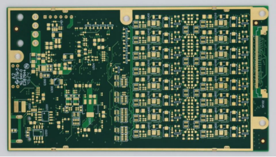
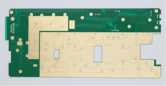
Multi-Layer PCBs
These PCBs have three or more layers of conductive traces separated by insulating layers. The layers are interconnected using vias, enabling high-density routing of electrical signals.
Pros:
Support high-density designs and complex circuit layouts.
Suitable for advanced applications requiring high-speed signal processing and miniaturization.
Cons:
More expensive and time-consuming to manufacture.
Higher risk of manufacturing defects due to increased complexity.
Example: Multi-layer PCBs are commonly found in smartphones, computers, and complex medical equipment, where multiple layers allow for compact designs and the integration of numerous components and functions.
Rigid, Flexible, and Rigid-Flex PCBs
PCBs can also be categorized by their physical structure, with the most common types being rigid, flexible, and rigid-flex boards.
Rigid PCBs
These are the most widely used type of PCB, made from a solid, inflexible material like fiberglass. Rigid PCBs provide robust mechanical support and are ideal for devices where the PCB must remain fixed in position.
Key Applications:
Industrial machinery: Rigid PCBs are used in control systems for machinery, where stability and durability are crucial.
Consumer electronics: Devices like desktop computers, gaming consoles, and televisions commonly use rigid PCBs.
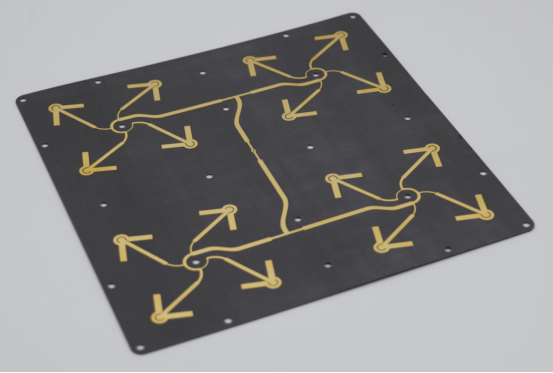
Flexible PCBs
Flexible PCBs are made from a flexible substrate, typically polyimide, allowing them to bend and conform to various shapes. These are ideal for applications where space is limited or a flexible form factor is required.
Key Applications:
Wearables: Devices like smartwatches, fitness trackers, and medical patches use flexible PCBs to accommodate small sizes and curved surfaces.
Foldable electronics: Flexible PCBs enable foldable phones, tablets, and screens, where the PCB needs to withstand bending without compromising functionality.
Rigid-Flex PCBs
Rigid-flex PCBs combine the features of both rigid and flexible PCBs. They consist of a combination of rigid and flexible sections, providing both structural support and flexibility in one design.
Key Applications:
Aerospace: Rigid-flex PCBs are used in avionics and satellite systems, where reliability and weight reduction are essential.
Medical devices: Rigid-flex PCBs are used in compact medical devices like hearing aids and pacemakers, where space constraints and durability are critical.
High-Density Interconnect (HDI) PCBs
HDI PCBs are a specialized type of multi-layer PCB designed to allow for high-density interconnections in a small space. These boards have smaller traces, more vias, and smaller component footprints, making them ideal for compact, high-performance devices.
What Makes HDI PCBs Different?
HDI PCBs use advanced manufacturing techniques to achieve higher circuit density on a smaller board. This includes finer traces, micro-vias, and blind or buried vias, which allow for greater miniaturization and performance in high-tech applications.
Typical Use Cases:
Smartphones: HDI PCBs are used in smartphones to pack more components into smaller spaces without sacrificing performance. This allows for better processing power and battery life in a compact form factor.
High-Performance Computing: Servers, high-end computers, and gaming consoles rely on HDI PCBs for faster data transmission and efficient use of space.
Benefits in Terms of Miniaturization and Performance:
Miniaturization: HDI PCBs allow for the creation of smaller, thinner devices with higher functionality, making them ideal for consumer electronics like wearables and IoT devices.
Performance: With their higher density, HDI PCBs enable faster signal processing, reducing the risk of signal loss and improving overall device performance.
PCB Manufacturing Process: A Step-by-Step Guide
The PCB manufacturing process is a highly detailed and intricate procedure that converts a design into a functional printed circuit board. Each step must be executed with precision to ensure the final product meets performance, reliability, and durability standards. Below is a detailed look at each phase of the manufacturing process.
Design and Layout
The design and layout phase is the foundation of PCB manufacturing, where engineers define how the components will fit onto the board and how they will be connected electrically.
Importance of Software Tools
To create an efficient PCB design, engineers rely on specialized software tools like Altium Designer, Eagle, and KiCad. These tools provide features that allow for precise component placement, electrical rule checking, and simulation of the electrical behavior of the design before it goes into production.
Key Considerations During the Design Phase
Several key factors must be taken into account when designing a PCB:
Trace Width: The width of the copper traces determines the current-carrying capacity of the PCB. Narrower traces can carry less current and are prone to overheating.
Spacing: Proper spacing between traces and pads is essential to prevent short circuits and ensure that components fit correctly.
Component Placement: Components should be placed to minimize signal interference and ensure easy routing of traces. High-frequency components should be placed close to each other to minimize signal loss.
Examples of Design Rules (DRC) and Their Impact on Manufacturing
Design Rule Check (DRC) is a process where the PCB layout is checked against a set of predefined design rules to ensure manufacturability. For example:
Minimum Trace Width: Ensures that traces are wide enough to handle the required current without overheating.
Via Sizes: Defines the minimum and maximum sizes for vias, which affect the number of layers and cost of the PCB.
DRC checks help avoid errors that could result in manufacturing defects or performance issues in the final PCB.
Materials Selection
Selecting the right materials for a PCB is crucial as it influences the board’s electrical, thermal, and mechanical properties. The most common PCB substrates include FR4, Rogers, and Polyimide.
Common PCB Substrate Materials
FR4: The most widely used PCB material, made from woven fiberglass and epoxy resin. It is cost-effective, offers good mechanical strength, and performs well in standard temperature ranges.
Rogers: A high-performance material that offers excellent electrical properties, especially for high-frequency applications. It’s often used in RF (Radio Frequency) and microwave PCBs.
Polyimide: Used in flexible PCBs, this material has excellent heat resistance and flexibility, making it ideal for applications in wearables or flexible electronics.
Comparison of Performance and Cost
FR4 is the most cost-effective choice for general applications, but it has limitations in terms of performance at high frequencies or extreme temperatures.
Rogers materials are more expensive but are essential for RF applications due to their low loss and high frequency handling capabilities.
Polyimide is also higher in cost but is indispensable in industries requiring flexible, high-temperature resistant solutions, such as aerospace and medical devices.
How Material Choice Affects Electrical, Thermal, and Mechanical Properties
The substrate material significantly affects the PCB's electrical performance (such as signal integrity and capacitance), its ability to dissipate heat (important for high-power applications), and its mechanical strength (important for durability in harsh environments). For example, Rogers materials can reduce signal loss, while Polyimide offers better performance in flexible and wearable devices.
Printing and Etching
In the printing and etching phase, the PCB design is transferred onto the substrate material, where copper traces are formed to connect the various components.
Overview of the Photolithographic Process
The process begins with applying a layer of photosensitive material (photoresist) to the copper surface. The PCB design is then exposed to ultraviolet (UV) light through a photomask, transferring the design onto the photoresist. The exposed areas are chemically developed, leaving the copper traces intact in the areas not exposed to light.
Step-by-Step Breakdown of Etching Copper Traces
Apply Photoresist: A thin layer of photoresist is spread over the PCB’s copper surface.
Exposure: The PCB is exposed to UV light through a photomask that defines the PCB traces.
Development: The exposed photoresist is washed away, leaving the design pattern on the PCB.
Etching: The unprotected copper is etched away using a chemical solution, leaving only the copper traces behind.
Example of High-Precision Etching for HDI PCBs
For HDI PCBs, the etching process is more precise due to smaller traces and finer features. High-precision etching techniques are used to ensure that smaller vias and tighter trace widths are maintained, crucial for high-performance applications like smartphones and high-speed communication systems.
Plating and Layering
Plating and layering are essential for building up the PCB, especially for multi-layer boards. These processes ensure the electrical connections are properly established between layers.
Plating Techniques
Electroless Plating: A process where copper is deposited onto the PCB without the need for an electric current. This is typically used to plate the vias in multi-layer PCBs.
Electroplating: Uses an electric current to deposit a layer of copper onto the PCB, primarily used to build up the copper thickness on pads and traces.
Layer Bonding in Multi-Layer PCBs
Multi-layer PCBs are created by bonding several layers of PCB material together with insulating layers in between. The layers are pressed together under heat and pressure to form a solid unit. Vias are drilled through the layers to allow electrical signals to pass between them.
Comparison of Through-Hole vs. Surface-Mount Technology (SMT) Processes
Through-Hole Technology (THT): Components are inserted into holes in the PCB and soldered from the opposite side. This method is typically used for larger, more durable components like connectors.
Surface-Mount Technology (SMT): Components are mounted directly on the surface of the PCB, which allows for smaller, lighter devices and faster manufacturing processes. SMT is commonly used in most modern electronic devices.
Testing and Quality Assurance
Once the PCB is fabricated, it undergoes a series of testing and quality assurance steps to ensure functionality and reliability.
Types of Tests Performed
Automated Optical Inspection (AOI): A machine-based inspection process that scans the PCB for defects such as misaligned components, soldering issues, and trace defects.
X-ray Inspection: Used for inspecting multi-layer PCBs and checking for issues such as voids in the solder joints or incomplete vias, particularly in high-density PCBs.
The Importance of Tolerance and Error-Checking
Tolerance refers to the allowable variations in the PCB’s dimensions, such as trace width and spacing. Tight tolerances are crucial in high-performance applications to avoid signal interference and ensure proper functionality. Error-checking during the manufacturing process is essential to catch and correct issues before the final product reaches the customer.
Examples of Failures and How They Are Mitigated
Common PCB manufacturing failures include solder bridging, where excess solder connects two pads, and open circuits, where traces are broken or incomplete. These issues are often mitigated through thorough testing, error-checking software, and careful inspection techniques, ensuring the board functions correctly and reliably.
Challenges in PCB Manufacturing and How to Overcome Them
PCB manufacturing is a highly complex process that involves numerous challenges at each stage, from design to production. Understanding these challenges and knowing how to address them is crucial for ensuring the production of high-quality, reliable printed circuit boards. Below are some of the key challenges in PCB manufacturing and strategies to overcome them.
Complexity in Design and Fabrication
As electronic devices become more sophisticated, the designs for their PCBs are also growing in complexity. High-density and multi-layer PCBs present significant challenges in terms of both design and fabrication.
Managing Complexity in High-Density and Multi-Layer Designs
High-density PCBs involve intricate designs with narrow traces, smaller components, and complex routing. Multi-layer PCBs add an additional layer of complexity, as multiple layers of circuitry need to be properly aligned, stacked, and interconnected.
Engineers must ensure that signals can travel across these layers without interference and that there is adequate power distribution for all components. Design software such as Altium and Eagle help manage this complexity by providing features like automatic routing, design rule checks (DRC), and multi-layer visualization.
Example of a Design Challenge in RF (Radio Frequency) PCBs
In RF PCBs, signal integrity is a critical concern. RF signals are highly susceptible to loss, interference, and reflection, which can degrade the performance of the electronic device. To overcome this, engineers use advanced design techniques, such as controlled impedance routing and careful placement of components to minimize signal path length.
Additionally, Rogers materials, with their superior high-frequency performance, are often used for RF PCB designs to ensure minimal signal loss.
Material Constraints
Choosing the right materials for PCB manufacturing is crucial, but it also presents challenges due to availability, cost, and performance requirements.
Availability and Cost of Advanced PCB Materials
While FR4 remains the most cost-effective and widely used PCB material, certain applications require specialized materials with superior electrical or thermal properties. Rogers materials, for example, are essential for high-frequency designs but come at a premium. As technology advances, the demand for materials that can handle higher power, thermal stress, and faster signal speeds is growing, yet these materials are often expensive and difficult to source in large quantities.
How Engineers Can Balance Performance and Cost When Selecting Materials
Engineers need to strike a balance between performance and cost when selecting PCB materials. In applications like consumer electronics, where performance is essential but cost is a significant concern, engineers often use a combination of materials. For instance, FR4 might be chosen for the bulk of the PCB, while more expensive materials like Polyimide or Rogers might be used for specific high-performance areas, such as the RF section of a device.
Case Study: PCB Materials Used in High-End Consumer Electronics
In high-end consumer electronics, such as smartphones or gaming consoles, multi-layer PCBs are commonly used with a mix of FR4 for general circuitry and Rogers for high-frequency components. This combination allows manufacturers to achieve the necessary performance for demanding tasks while keeping costs in check.
Environmental and Regulatory Considerations
Environmental and regulatory challenges are also an important consideration in PCB manufacturing. Regulations like RoHS and WEEE ensure that PCBs are produced in ways that minimize environmental harm.
Regulations like RoHS and WEEE that Affect PCB Manufacturing
RoHS (Restriction of Hazardous Substances) is a key regulation that limits the use of harmful materials in PCB manufacturing, such as lead, mercury, and cadmium. WEEE (Waste Electrical and Electronic Equipment) focuses on the recycling and disposal of electronic products.
PCB manufacturers must ensure compliance with these regulations by using lead-free soldering and adopting sustainable disposal practices for end-of-life electronics.
Environmental Challenges and Sustainable Practices in PCB Production
PCB manufacturing can be resource-intensive, with waste materials, energy consumption, and water usage contributing to environmental impact. Sustainable practices, such as using eco-friendly soldering materials, reducing chemical waste, and implementing energy-efficient manufacturing processes, are becoming more widespread. Companies are increasingly adopting these practices to reduce their carbon footprint and adhere to global environmental standards.
Examples of Eco-Friendly PCB Innovations
Lead-Free Soldering: With the rise of RoHS regulations, lead-free soldering has become a standard practice. Materials like tin-silver-copper (SAC) solder are now commonly used in place of traditional lead-based solder.
Eco-Friendly PCB Laminates: Some manufacturers are turning to bio-based resins for PCB laminates, which are made from renewable materials and are less harmful to the environment during production and disposal.
Production Yield and Scalability
Achieving a high production yield and scaling manufacturing for large volumes is a constant challenge in PCB production.
Factors Influencing Production Yield
The yield in PCB manufacturing refers to the percentage of boards that meet quality standards after production. Factors that influence yield include:
Design Defects: Mistakes in the initial design, such as incorrect trace widths or inadequate spacing, can result in a high failure rate.
Material Inconsistencies: Variability in the quality of materials, such as copper thickness or substrate uniformity, can lead to defects in the final product.
Production Process Variability: Inconsistent processes, like improper soldering or etching, can cause issues like misalignment or solder bridges, impacting yield.
How to Improve Yield in Large-Scale Manufacturing
To improve yield, manufacturers implement rigorous testing and quality control measures. Automated Optical Inspection (AOI) systems help detect defects early in the production process, while Design for Manufacturability (DFM) guidelines ensure that the design is optimized for high yields. Engineers also work closely with PCB manufacturers to standardize processes and minimize errors during assembly.
Best Practices for Transitioning from Prototype to Mass Production
Transitioning from prototype to mass production requires careful planning to maintain quality while scaling up production. Engineers should:
Conduct thorough testing on prototypes to identify potential issues before large-scale manufacturing begins.
Ensure that the design is optimized for automated production, minimizing manual intervention.
Establish clear communication channels between design teams and manufacturing partners to address issues quickly and efficiently.
Advanced Trends in PCB Manufacturing
PCB manufacturing is evolving rapidly, driven by the increasing demands for smaller, more powerful, and more complex electronic devices. In this section, we will explore some of the key trends reshaping the industry, including miniaturization, the integration of 3D printing, and the use of AI and automation in production.
Miniaturization and Multi-Functional PCBs
The ongoing trend toward miniaturization and the development of multi-functional PCBs is transforming how electronic devices are designed and manufactured. As consumer and industrial devices become smaller and more powerful, PCBs are expected to meet more stringent size and functionality requirements.
The Trend Toward Smaller, Lighter, and More Powerful PCBs
Miniaturization is pushing the boundaries of PCB design, with boards becoming increasingly compact while still maintaining or enhancing their capabilities. This trend is driven by the need for portable, efficient, and lightweight devices like smartphones, wearables, and IoT (Internet of Things) products. For example, today’s smartphones have more advanced features packed into thinner, lighter designs, all powered by high-performance, miniaturized PCBs.
Examples of Multi-Functional PCBs in IoT Devices and Wearables
Multi-functional PCBs combine various functions into a single board, allowing for smaller form factors without sacrificing performance. In IoT devices, for instance, a PCB might integrate sensors, power management circuits, communication modules (like Bluetooth or Wi-Fi), and processing components, all within a small package. In wearables like smartwatches, multi-functional PCBs allow for the integration of health tracking, GPS, and wireless communication, all in a compact, flexible design.
Challenges and Solutions in Miniaturization
As PCBs shrink in size, new challenges emerge, particularly with high-density components and the need for tiny traces. In high-density PCBs, the narrow trace widths and tight component spacing must be precisely engineered to avoid short circuits or signal interference. Solutions to these challenges include the use of HDI (High-Density Interconnect) PCBs, which allow for finer traces, micro-vias, and multi-layer stacking to manage increased complexity and maintain signal integrity. Additionally, advanced materials such as flexible substrates and low-loss laminates are used to improve performance in miniaturized designs.
Integration of 3D Printing and Additive Manufacturing
The integration of 3D printing and additive manufacturing in PCB production is revolutionizing how prototypes are developed and small-batch PCBs are produced.
How 3D Printing is Being Used to Prototype and Even Produce Certain Types of PCBs
3D printing allows for the rapid prototyping of PCBs by building up layers of material (such as conductive inks) to form the traces, components, and connections. This method provides greater design flexibility and can significantly shorten the time required for prototyping compared to traditional PCB manufacturing processes, which require the creation of photomasks and etching.
Moreover, certain types of additive manufacturing are used to print flexible PCBs, where conductive materials can be printed onto flexible substrates. This is particularly beneficial for applications requiring conformable circuits, such as in wearable electronics and flexible displays.
Benefits of Additive Manufacturing for Rapid Prototyping and Low-Volume Production
Additive manufacturing excels in rapid prototyping due to its ability to quickly create prototypes for testing and design iterations. It’s especially useful in low-volume production, as it eliminates the need for costly and time-consuming tooling, making it an ideal choice for niche or customized PCB designs.
Case Study: A Company Using 3D Printing to Create Flexible PCBs for a Wearable Tech Product
A prominent wearable tech company has begun using 3D printing to create flexible PCBs for their fitness trackers. By leveraging additive manufacturing, the company can produce flexible PCBs that conform to the contours of the human body, improving the comfort and wearability of the device. This approach also reduces lead times and manufacturing costs, allowing for rapid prototyping and iteration during the product development cycle.
AI and Automation in PCB Production
The use of Artificial Intelligence (AI) and automation is transforming PCB manufacturing, offering new possibilities for design optimization, error reduction, and faster production cycles.
Role of AI in Optimizing PCB Design and Manufacturing Processes
AI plays a pivotal role in optimizing PCB design by helping engineers quickly identify potential design flaws and optimize layouts. AI-based tools can analyze vast amounts of design data and predict the electrical and thermal performance of a PCB before it is even manufactured. This helps engineers make smarter decisions regarding trace widths, component placement, and power distribution, resulting in more reliable and efficient boards.
In manufacturing, AI is also used to monitor production processes, automatically adjusting parameters such as temperature, pressure, or time to improve quality and consistency across batches. Machine learning algorithms can even detect patterns in defects and suggest adjustments to avoid future issues, reducing the likelihood of faulty boards reaching customers.
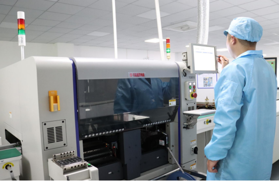
Automation in Assembly Lines for High-Speed Production and Error Reduction
Automation in PCB assembly lines allows for high-speed production while minimizing human error. Robotic arms and automated pick-and-place machines handle component placement and soldering, increasing speed and accuracy. Additionally, automated inspection systems use optical sensors to detect defects during the assembly process, such as misaligned components, soldering errors, or insufficient solder joints. This reduces the need for manual inspection and enhances the reliability of the final product.
Example of Automated Inspection Systems in Modern PCB Factories
Modern PCB factories utilize automated optical inspection (AOI) systems to check for defects at various stages of the manufacturing process. AOI systems capture high-resolution images of the PCB surface and compare them to a reference image to identify any discrepancies. These systems can quickly detect issues like trace defects, missing components, or improper solder joints, allowing for quick corrections before production continues.
Key Considerations for Engineers When Selecting PCB Manufacturers
Selecting the right PCB manufacturer is a critical decision that can significantly impact the performance, cost, and timeline of your electronic projects. Engineers need to carefully evaluate manufacturers based on several key factors to ensure the best possible outcome for their designs.
Choosing the Right Manufacturer for Your Needs
When selecting a PCB manufacturer, it's essential to evaluate potential candidates using several key criteria that align with your project's specific needs.
Criteria to Evaluate Potential PCB Manufacturers
Engineers should consider several factors when assessing a manufacturer:
Certifications: Look for manufacturers that hold relevant industry certifications such as ISO 9001 for quality management, UL for safety, and RoHS compliance for environmental standards. These certifications ensure the manufacturer adheres to recognized industry standards and quality controls.
Experience: A manufacturer with a proven track record in the specific type of PCB you need (e.g., multi-layer PCBs, flexible PCBs, or HDI boards) will be more likely to meet your expectations and handle complex designs effectively.
Production Capabilities: Ensure the manufacturer can handle the design complexity, material requirements, and production volume needed for your project. Ask about their capability to produce high-density boards or specialty materials if your design demands these.
How to Assess the Manufacturer’s Ability to Meet Quality Standards and Timelines
Before finalizing a manufacturer, it's important to assess how well they meet quality standards and deadlines.
Quality Assurance: Look for manufacturers with a robust quality control system in place. Ask for their approach to Automated Optical Inspection (AOI), X-ray inspection, and other quality assurance measures.
Timeliness: Confirm the manufacturer’s lead times for both prototypes and full production runs. Ensure they can meet your project’s timeline by discussing specific deadlines and understanding their capacity for scaling production as needed.
Cost vs. Quality: Striking the Right Balance
PCB production often involves a balancing act between cost and quality. While it's tempting to opt for cheaper manufacturing options, sacrificing quality can lead to significant performance and reliability issues down the line.
Factors that Influence Cost in PCB Production
Several factors contribute to the overall cost of PCB production:
Material Choice: High-performance materials like Rogers or Polyimide tend to be more expensive than standard FR4 materials. If your design requires advanced substrates, expect a higher cost.
Design Complexity: Complex PCB designs, such as those requiring multi-layer boards, fine traces, or high-density interconnects (HDI), will increase manufacturing costs due to the increased precision required in fabrication.
Volume: Larger production runs generally lower the per-unit cost due to economies of scale, while smaller batch productions often result in higher costs per unit.
How to Make Cost-Effective Decisions Without Compromising Quality
Engineers can optimize costs without sacrificing quality by considering these strategies:
Material Selection: Choose cost-effective materials for non-critical sections of the PCB. For example, use FR4 for general-purpose boards, while reserving higher-end materials for specific functions like high-frequency circuits or thermal management.
Design for Manufacturability (DFM): Simplify the PCB design where possible. Avoid overly complex routing or intricate features that would significantly increase production costs. Work with the manufacturer to ensure your design is optimized for mass production.
Prototype Testing: Instead of committing to a large production run, consider producing smaller quantities of prototypes first to identify potential issues early on and prevent costly errors in mass production.
Communication and Collaboration with Manufacturers
Effective communication and collaboration between engineers and manufacturers are essential to ensure that the design specifications are met, and any potential issues are addressed early in the process.
Importance of Clear Communication in Ensuring Design Specifications Are Met
Clear communication ensures that the manufacturer fully understands the design intent, including material choices, layer count, trace widths, and specific tolerances. Misunderstandings at this stage can lead to costly delays or production defects. It’s important to provide detailed documentation and collaborate with the manufacturer early in the design phase.
How Engineers Can Work Closely with Manufacturers to Solve Potential Design or Production Issues
Engineers should maintain an open line of communication with manufacturers during the production process. If any issues arise during prototyping or testing, working closely with the manufacturer can help identify solutions quickly. For example, if a design rule violation is discovered, engineers can work with the manufacturer to adjust the design or production methods to resolve the issue.
In some cases, engineers may need to participate in design reviews or pre-production meetings to ensure that all aspects of the design are thoroughly understood and executable. Regular feedback and updates will help ensure that the final PCB meets the performance and quality requirements.
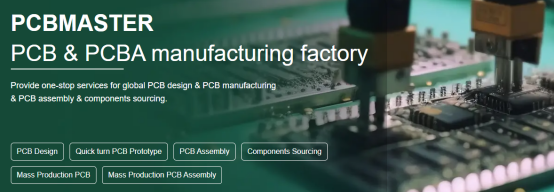
Recommended Manufacturer: PCBMASTER
When choosing a PCB manufacturer, PCBMASTER stands out for its commitment to high-quality, reliable, and cost-effective PCB production. Whether you need high-performance multi-layer boards or flexible PCBs for wearables, PCBMaster offers a range of services designed to meet the demands of today’s complex electronic devices. Their ability to handle both low-volume prototypes and large-scale production runs ensures that you can confidently scale your project, with the assurance that quality will never be compromised. From rapid prototyping to final production, PCBMaster provides the expertise and support to bring your designs to life.
Conclusion
The future of PCB manufacturing is defined by miniaturization, sustainability, and integration with emerging technologies. As devices become smaller and more powerful, PCBs must evolve to support these changes. Miniaturization continues to push the need for high-density and multi-layer boards, particularly in wearables and IoT devices. Sustainability also takes center stage, with manufacturers adopting eco-friendly materials and processes to meet environmental standards like RoHS. Additionally, technologies such as 3D printing and AI are revolutionizing how PCBs are designed and produced, offering faster prototyping, greater flexibility, and enhanced manufacturing efficiency.
To stay ahead, engineers need to keep up with these trends, ensuring they’re well-versed in new materials, production techniques, and automation tools. Close collaboration with manufacturers is crucial to optimize designs, reduce costs, and maintain high quality. The ability to adapt and innovate in PCB design and production will be key to supporting the future of electronics, ensuring reliable, high-performance devices for years to come.
FAQs
What are the most common materials used in PCB manufacturing?
The most common materials used in PCB manufacturing are:
FR4 (Flame Retardant 4): This is the most widely used substrate material for PCBs. It’s a composite of woven fiberglass and epoxy resin, offering a good balance of strength, durability, and cost-effectiveness for most general applications.
CEM1 and CEM3: These are alternative materials, often used in lower-cost, simpler PCBs. CEM1 is a single-sided PCB material, while CEM3 is a more durable, multi-layer substrate.
Polyimide: Used for flexible PCBs, polyimide offers excellent thermal stability and flexibility, making it ideal for applications where the board needs to bend or flex.
Rogers: Known for its high-frequency applications, Rogers materials are commonly used in RF (Radio Frequency) and microwave PCBs due to their superior performance in high-speed, high-frequency environments.
Aluminum: Used in metal-core PCBs for applications that require heat dissipation, such as power electronics or LED lighting.
Each material has specific advantages depending on the application’s performance, thermal, and electrical requirements.
How do engineers ensure the reliability of PCBs in complex electronics?
Ensuring the reliability of PCBs in complex electronics involves a multi-faceted approach:
Design Validation: Engineers use simulation tools to verify the design before production. Software like Altium and Eagle allows for thorough testing of electrical and thermal behavior.
Material Selection: Choosing the right materials for specific environments and applications, such as high-frequency or high-temperature conditions, helps prevent failure.
Manufacturing Process Control: Tight control over the manufacturing process, including precise etching, soldering, and layer bonding, ensures the board performs as expected.
Stress Testing: Engineers subject PCBs to various stress tests, including thermal cycling, vibration tests, and shock testing, to simulate real-world conditions and identify potential failure points.
Redundancy: In critical applications, engineers often incorporate design elements like redundant traces or dual-layer protection to ensure that a failure in one part of the PCB doesn’t lead to total failure of the device.
What are the environmental impacts of PCB manufacturing and how can they be minimized?
PCB manufacturing can have significant environmental impacts, primarily through the use of toxic materials and energy consumption. Some key environmental concerns include:
Toxic chemicals: Lead, cadmium, and solvents used in PCB production can be hazardous to both human health and the environment if not disposed of properly.
Energy and water consumption: The production process often involves high energy usage and water waste during various stages like etching and washing.
To minimize these impacts:
RoHS Compliance: The Restriction of Hazardous Substances (RoHS) directive limits the use of harmful materials like lead, mercury, and cadmium in PCBs, pushing manufacturers to adopt lead-free soldering and alternative materials.
Sustainable Manufacturing: PCB manufacturers are increasingly using eco-friendly processes like water-based etching and energy-efficient equipment to reduce the environmental footprint.
Recycling and Waste Management: Companies are also investing in closed-loop systems for waste recovery and promoting the recycling of end-of-life PCBs to reduce landfill waste.
How does the choice of PCB design software affect the manufacturing process?
The choice of PCB design software directly influences the manufacturing process, as it determines how easily the design can be translated into a finished product. Key factors include:
Design Precision: High-quality design software like Altium or Cadence provides tools for precise trace routing, component placement, and layer management, ensuring the design can be manufactured without issues.
Design for Manufacturability (DFM): Some software offers DFM checks that help engineers identify potential issues that might arise during the manufacturing process, such as unrealistic trace widths or inadequate component spacing.
File Generation: Software can generate the necessary files (e.g., Gerber files) that are used for PCB fabrication. The software’s ability to produce accurate and error-free files directly impacts the efficiency and quality of the manufacturing process.
Simulation: Advanced software provides simulation capabilities to predict how the PCB will perform under real-world conditions, helping to avoid costly production rework.
Choosing the right design software can streamline the process, reduce errors, and save time in PCB production.
What are the best practices for troubleshooting and repairing defective PCBs during production?
Troubleshooting and repairing defective PCBs during production require a systematic approach:
Visual Inspection: The first step is to conduct a visual inspection using tools like automated optical inspection (AOI) or microscopes to identify visible defects like misaligned components, solder bridges, or broken traces.
Testing: Electrical testing, such as continuity testing and in-circuit testing (ICT), can help identify issues with electrical connections or faulty components.
Rework and Repair: Once defects are identified, rework stations with precision tools, such as soldering irons or hot air rework stations, are used to fix issues like poor solder joints or damaged components.
Documenting Defects: Keep a log of common defects to identify any recurring issues that may stem from the design or manufacturing process. This information can help improve future production runs.
Quality Control Feedback: Engage in feedback loops with the design team and manufacturer to ensure that issues are caught early and resolved before they affect large batches of PCBs.
Following these best practices can help reduce production downtime and improve the overall quality of PCBs.

