


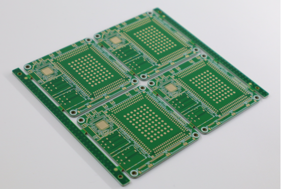
Essential HDI PCB Materials: Dielectrics, Copper Foils, Reinforcements, and Surface Finishes
HDI (High-Density Interconnect) PCBs are essential for powering the latest generation of electronic devices, from smartphones to medical implants. These advanced circuit boards are built with fine-pitch traces, microvias, and multiple layers, allowing for faster and more reliable performance in compact designs. The materials used in HDI boards are key to their success. Dielectric substrates control signal integrity and reduce loss, copper foils enable the creation of ultra-fine traces, and reinforcement materials provide mechanical strength for multi-layer structures, while surface finishes protect the copper from oxidation and ensure reliable soldering for smaller components. Together, these materials ensure HDI boards can handle the demands of high-frequency and high-speed applications, making them indispensable for everything from 5G networks to wearable technology. Understanding the role of each material is crucial for optimizing design and performance in these high-tech products.
Dielectric Substrates in HDI PCBs: The Foundation for Signal Integrity
In HDI PCB designs, dielectric substrates play a crucial role in ensuring signal integrity. These materials separate the conductive layers of the board, controlling the speed and quality of signals transmitted between them. The key properties of dielectric materials—Dielectric Constant (Dk), Dissipation Factor (Df), and Glass Transition Temperature (Tg)—directly influence the performance of the PCB.
Key Properties of Dielectric Materials in HDI
Dielectric Constant (Dk): This property measures the material's ability to store electrical energy. A low Dk is preferred in high-speed applications to minimize signal delay and maintain high-frequency performance. Materials with a Dk of around 3.0–4.5 are commonly used in HDI PCBs.
Dissipation Factor (Df): Df indicates how much energy is lost as heat during signal transmission. Lower Df values reduce signal loss and improve the efficiency of the PCB, which is especially important in high-frequency applications where signal quality is critical.
Glass Transition Temperature (Tg): Tg represents the temperature at which a material transitions from a rigid to a flexible state. Higher Tg ensures that the material can handle high temperatures without degrading. This is particularly important in automotive and industrial applications, where the PCB may be exposed to harsh conditions.
Together, these properties determine how well a dielectric material can support high-speed signals, low loss, and thermal stability—key factors for performance in HDI PCB designs.
Material Categories for HDI PCBs
There are several types of dielectric materials used in HDI PCBs, each suited to specific applications. Below are some of the most commonly used materials:
Advanced FR4
Usage: Consumer electronics, IoT sensors
Properties: Advanced FR4 offers a balanced combination of cost-effectiveness, moderate dielectric constant (Dk), and low dissipation factor (Df). It is the go-to material for most consumer electronic devices.
Example: FR4 is frequently used in smartphones and home appliances, where cost, moderate performance, and high manufacturability are crucial.
Polyimide
Usage: Flexible HDI, wearables, automotive sensors
Properties: Polyimide is known for its high-temperature resistance and flexibility. It has a low Dk and Df, making it ideal for flexible HDI designs that need to withstand harsh environments.
Example: Polyimide is commonly found in wearable devices and automotive sensors, where flexibility and temperature tolerance are vital.
BT-Epoxy (Bismaleimide-Triazine)
Usage: Automotive ADAS, 5G base stations
Properties: BT-epoxy offers excellent moisture resistance and dimensional stability, making it ideal for high-reliability applications like automotive electronics and 5G base stations.
Example: BT-epoxy is used in Advanced Driver Assistance Systems (ADAS), where performance consistency is critical even in extreme temperatures.
PTFE (Polytetrafluoroethylene)
Usage: mmWave radar, satellite communication
Properties: PTFE has an ultra-low dissipation factor (Df) and high-frequency performance, making it the best material for high-speed, high-frequency applications like mmWave radar and satellite communication.
Example: PTFE is widely used in 5G communications and radar systems, where low signal loss and high frequency are crucial for reliable performance.
ABF (Ajinomoto Build-up Film)
Usage: High-density IC substrates, server CPUs
Properties: ABF film is known for its ability to handle ultra-fine lines and its highly stable dielectric constant (Dk). It is mainly used in high-density interconnects for advanced IC packaging.
Example: ABF is commonly used in server CPUs and high-performance computing applications, where fine trace widths and precise signal integrity are essential.
Summary Table
| Material | Usage | Properties | Example |
| Advanced FR4 | Consumer electronics, IoT sensors | Cost-effective, moderate dielectric constant (Dk), low dissipation factor (Df) | Used in smartphones and home appliances for cost and manufacturability. |
| Polyimide | Flexible HDI, wearables, automotive sensors | High-temperature resistance, flexibility, low Dk and Df | Common in wearables and automotive sensors, where flexibility and temperature tolerance are critical. |
| BT-Epoxy (Bismaleimide-Triazine) | Automotive ADAS, 5G base stations | Excellent moisture resistance, dimensional stability | Found in ADAS and 5G base stations, where high reliability in extreme conditions is essential. |
| PTFE (Polytetrafluoroethylene) | mmWave radar, satellite communication | Ultra-low Df, high-frequency performance | Used in 5G communications and radar systems, crucial for low signal loss and high-frequency performance. |
| ABF (Ajinomoto Build-up Film) | High-density IC substrates, server CPUs | Ultra-fine line capability, highly stable dielectric constant (Dk) | Common in server CPUs and high-performance computing, where precise signal integrity is required. |
Performance Breakdown by Frequency
The choice of dielectric material also depends on the frequency range of the application. Different materials perform better at different frequencies due to their Dk and Df properties:
<10GHz (e.g., Wi-Fi, Bluetooth): For lower-frequency applications, such as Wi-Fi and Bluetooth, advanced FR4 and BT-epoxy are suitable due to their balanced Dk/Df properties. These materials offer a cost-effective solution for devices operating in the sub-10GHz range.
10–30GHz (e.g., 5G sub-6GHz): For mid-range frequencies like those used in 5G sub-6GHz applications, materials like BT-epoxy and polyimide provide the right balance of low signal loss and thermal stability. These materials ensure reliable performance in next-generation mobile networks.
>30GHz (e.g., mmWave frequencies): For high-frequency applications above 30GHz, such as mmWave radar and satellite communications, materials like PTFE and ABF are ideal. These materials minimize signal attenuation and provide high-performance support for extremely fast data transmission.
Each material's suitability for different frequency ranges is essential for ensuring signal integrity, reducing loss, and optimizing performance in high-speed electronic devices. Understanding these properties helps engineers choose the right material for the right application.
Copper Foils: Ensuring Fine Traces and Low Signal Loss
Copper foils are essential for creating the electrical pathways in HDI PCBs. The quality of these foils directly impacts signal integrity and the performance of high-frequency devices. As the demand for faster, smaller, and more efficient electronics grows, so does the need for specialized copper foils that can support fine traces, microvias, and high-frequency signals with minimal loss.
Copper Foil Types for HDI PCBs
There are several types of copper foils used in HDI PCB manufacturing, each suited to specific applications based on their thickness and surface characteristics.
Thin Copper Foils
Thickness: 9–18μm (0.25–0.5oz)
Surface Roughness: Moderate (0.5–1.0μm)
Applications: Thin copper foils are commonly used in consumer electronics like smartphones and wearables, where space is limited and high-density interconnections are required.
Example: In smartphones, thin copper foils allow the PCB to accommodate more components without increasing size, ensuring reliable signal transmission in compact designs.
Ultra-Smooth Copper
Thickness: 12–35μm (0.35–1oz)
Surface Roughness: Ultra-low (< 0.1μm)
Applications: Ultra-smooth copper is used in high-frequency applications like mmWave antennas and 5G transceivers, where minimal signal degradation is crucial.
Example: In 5G transceivers, ultra-smooth copper reduces signal loss at high frequencies, ensuring reliable communication at speeds over 10Gbps.
Rolled Annealed (RA) Copper
Thickness: 18–70μm (0.5–2oz)
Surface Roughness: Low (0.3–0.5μm)
Applications: RA copper is used in applications that require flexibility, such as automotive sensors and foldable displays. Its ability to bend without cracking makes it ideal for flexible HDI PCBs.
Example: In foldable displays, RA copper allows the PCB to maintain performance even as the device bends and flexes.
Summary Table
| Copper Foil Type | Thickness | Surface Roughness | Applications | Example |
| Thin Copper Foils | 9–18μm (0.25–0.5oz) | Moderate (0.5–1.0μm) | Consumer electronics like smartphones and wearables, where space is limited. | In smartphones, thin copper foils allow the PCB to accommodate more components without increasing size. |
| Ultra-Smooth Copper | 12–35μm (0.35–1oz) | Ultra-low (< 0.1μm) | High-frequency applications like mmWave antennas and 5G transceivers. | In 5G transceivers, ultra-smooth copper reduces signal loss, ensuring reliable communication at speeds over 10Gbps. |
| Rolled Annealed (RA) Copper | 18–70μm (0.5–2oz) | Low (0.3–0.5μm) | Flexible HDI applications such as automotive sensors and foldable displays. | In foldable displays, RA copper maintains performance even as the device bends and flexes. |
Impact of Surface Roughness on High-Frequency Signals
Surface roughness is a critical factor in high-frequency signal transmission. At high frequencies, like those used in mmWave (60GHz) applications, the electrical current primarily flows along the surface of the copper. If the copper surface is rough, it can scatter the signal, causing additional loss and interference. Ultra-smooth copper, with its low surface roughness (less than 0.1μm), reduces this scattering and helps maintain the integrity of high-frequency signals.
For example, when comparing two copper foils at 60GHz, a rougher surface can increase signal loss by as much as 30% compared to ultra-smooth copper. This is especially important in applications like 5G and radar systems, where even slight signal degradation can result in poor performance.
Innovations in Copper Foil Manufacturing
Recent advancements in copper foil manufacturing focus on reducing signal degradation and improving performance in HDI designs. Ultra-thin copper foils, combined with innovative surface treatments, help achieve finer traces and better signal integrity. These innovations allow for more efficient use of PCB space and ensure that signals remain stable even at high frequencies.
For example, electrolytic copper plating is a common treatment used to enhance the smoothness of copper surfaces. This process helps create a more uniform surface, reducing roughness and minimizing signal loss. Additionally, the development of thin copper foils (down to 9μm) enables even tighter layouts, which is crucial for compact, high-density devices like wearables and medical implants.
These innovations are essential as the industry pushes for faster, more reliable electronics. By reducing the resistance and loss in copper pathways, manufacturers can ensure that HDI PCBs perform well even in the most demanding applications, such as 5G, IoT devices, and automotive electronics.
Reinforcement Materials: Structural Integrity and Process Compatibility
Reinforcement materials in HDI PCB manufacturing are crucial for ensuring the structural strength, reliability, and compatibility of multi-layer boards. These materials support the overall integrity of the PCB, help manage thermal expansion, and enable the creation of microvias, which are essential for high-density interconnections. Understanding the role of these reinforcements is key to ensuring the performance and durability of HDI PCBs in demanding applications.
Role of Reinforcements in HDI Manufacturing
In HDI PCBs, reinforcements provide the mechanical strength needed to support multiple layers, especially when dealing with the challenges of miniaturization and complex routing. As PCBs become thinner and more densely packed, the demand for strong yet lightweight materials increases. Reinforcement materials help in the following ways:
Mechanical Strength: Reinforcements add rigidity to the PCB, preventing deformation and ensuring that the PCB retains its shape under mechanical stress. This is particularly important in multi-layer HDI designs, where each layer must remain intact during manufacturing and operation.
Laser Drillability: In HDI PCBs, microvias are essential for connecting different layers. Reinforcement materials must be compatible with laser drilling, which is commonly used to create microvias. Materials that allow clean, precise drilling without excessive smearing or debris are critical for maintaining signal integrity.
Thermal Stability: High-performance HDI boards are often exposed to heat, which can cause warping or thermal expansion. Reinforcement materials help manage these effects by providing a stable structure that resists warpage, ensuring long-term reliability.
Types of Reinforcement Materials
Several types of reinforcement materials are used in HDI PCB manufacturing, each offering specific benefits that suit different applications. Below are the most commonly used reinforcement materials:
Laser-Drillable Glass
Material: Spread glass yarns
Benefit: Laser-drillable glass simplifies the process of creating microvias, ensuring minimal drill smearing. This allows for more precise and cleaner microvias, which is essential for maintaining signal integrity in high-density designs.
Example: Laser-drillable glass is widely used in consumer electronics and mobile devices, where tight tolerances and small vias are required for efficient signal routing and miniaturized designs.
High-Strength Glass (E-glass)
Material: Low Coefficient of Thermal Expansion (CTE)
Benefit: E-glass offers high strength and a low coefficient of thermal expansion (CTE). This reduces the risk of warping during manufacturing, making it ideal for multi-layer HDI designs that are exposed to high temperatures during the soldering process.
Example: E-glass is commonly used in automotive electronics, where stability and thermal resistance are crucial for ensuring long-term performance in harsh environments.
Low-Dk Glass (S-glass)
Material: Reduced Dielectric Constant (Dk)
Benefit: S-glass has a lower dielectric constant (Dk) compared to E-glass, making it more suitable for high-frequency applications. This reduces signal loss, which is critical for applications like mmWave communications and radar systems.
Example: S-glass is used in advanced communication systems, such as 5G and radar technologies, where minimizing signal degradation at high frequencies is essential.
Summary Table
| Reinforcement Material | Material Characteristics | Benefit | Example |
| Laser-Drillable Glass | Spread glass yarns | Simplifies microvia creation with minimal drill smearing, ensuring clean and precise microvias. | Widely used in consumer electronics and mobile devices, where tight tolerances and small vias are needed. |
| High-Strength Glass (E-glass) | Low Coefficient of Thermal Expansion (CTE) | High strength and thermal resistance reduce warping during manufacturing, ideal for multi-layer designs. | Common in automotive electronics, where stability and resistance to high temperatures are essential. |
| Low-Dk Glass (S-glass) | Reduced Dielectric Constant (Dk) | Lower Dk reduces signal loss, making it ideal for high-frequency applications. | Used in advanced communication systems such as 5G and radar, where signal degradation must be minimized. |
Surface Finishes and Solder Masks: Enhancing Durability and Signal Integrity
In HDI PCB manufacturing, surface finishes and solder masks are essential for ensuring both the durability and functionality of the board. These elements protect the copper traces from corrosion, improve soldering performance, and play a key role in signal integrity, especially in high-speed, high-density applications. Proper selection of surface finishes and solder masks ensures the reliability of the final product, whether it’s for consumer electronics, automotive systems, or communication devices.
Surface Finish Types for HDI PCBs
Surface finishes are applied to the copper traces of PCBs to protect them from oxidation and improve their solderability. Different types of surface finishes offer distinct advantages based on the specific application needs. Below are the most commonly used surface finishes for HDI PCBs:
ENIG (Electroless Nickel Immersion Gold)
Key Advantage: ENIG provides a flat surface with excellent corrosion resistance, ensuring high reliability in harsh environments. This finish is ideal for fine-pitch ball grid arrays (BGAs) and high-frequency traces, where a smooth, consistent surface is essential for performance.
Best for: Fine-pitch BGAs and high-frequency applications, such as communication devices.
Example: ENIG is commonly used in smartphones, laptops, and high-speed communication systems, where precise soldering and signal integrity are critical.
Immersion Silver
Key Advantage: This finish offers a smooth surface that reduces signal loss, making it suitable for high-speed, high-frequency designs.
Best for: 5G RF modules, radar systems, and other high-frequency applications.
Example: Immersion silver is often used in 5G RF modules and radar systems where minimal signal attenuation is required for reliable performance.
ENEPIG (Electroless Nickel Electroless Palladium Immersion Gold)
Key Advantage: ENEPIG provides strong adhesion, high reliability, and excellent corrosion resistance, making it ideal for critical, high-performance applications.
Best for: Automotive Advanced Driver Assistance Systems (ADAS), aerospace, and other demanding environments.
Example: ENEPIG is widely used in automotive electronics, where the PCB must endure extreme conditions while maintaining electrical and mechanical stability.
Immersion Tin
Key Advantage: Immersion tin is cost-effective and provides good solderability, making it an economical option for high-density interconnects (HDI) without sacrificing performance.
Best for: Consumer electronics and low-cost HDI applications.
Example: Immersion tin is commonly used in consumer electronics such as TVs, wearables, and IoT devices, where cost-efficiency and reliable soldering are needed.
Summary Table
| Surface Finish | Key Advantage | Best For | Example |
| ENIG (Electroless Nickel Immersion Gold) | Flat surface with excellent corrosion resistance, ensuring high reliability in harsh environments. Ideal for fine-pitch BGAs and high-frequency traces. | Fine-pitch BGAs, high-frequency applications | Used in smartphones, laptops, and high-speed communication systems for precise soldering and signal integrity. |
| Immersion Silver | Smooth surface that reduces signal loss, making it suitable for high-speed, high-frequency designs. | 5G RF modules, radar systems, high-frequency applications | Often used in 5G RF modules and radar systems, ensuring minimal signal attenuation for reliable performance. |
| ENEPIG (Electroless Nickel Electroless Palladium Immersion Gold) | Strong adhesion, high reliability, and excellent corrosion resistance, ideal for critical, high-performance applications. | Automotive ADAS, aerospace, demanding environments | Widely used in automotive electronics, where the PCB must endure extreme conditions while maintaining stability. |
| Immersion Tin | Cost-effective, good solderability, making it economical for HDI applications without sacrificing performance. | Consumer electronics, low-cost HDI applications | Common in consumer electronics such as TVs, wearables, and IoT devices, where cost-efficiency and reliable soldering are required. |
Solder Mask Technologies
Solder masks are used to cover areas of the PCB that should not be soldered, ensuring that solder does not bridge between adjacent traces. These masks also help protect the PCB from environmental factors and improve the overall reliability of the board. There are two main types of solder mask technologies used in HDI PCBs:
LPI (Liquid Photo-Imaginable)
Feature: LPI solder mask provides high resolution, which is essential for fine-pitch components and microvias. This technology is highly flexible and ideal for creating PCBs with complex layouts.
Applications: Smartphones, IoT devices, and other consumer electronics where small components and microvias are used.
Example: LPI is frequently used in smartphones, where it allows for high-density designs with very fine pitch components and precise microvias.
LDI (Laser Direct Imaging)
Feature: LDI technology uses lasers to precisely align the solder mask with laser-drilled features, enabling very fine trace and space dimensions. This is crucial for HDI designs with microvias and high-density interconnects.
Applications: High-density HDI designs with microvias, such as advanced communications devices and servers.
Example: LDI is commonly used in high-speed computing systems and telecom infrastructure, where precise alignment is necessary for ensuring high reliability and performance.
Summary Table
| Solder Mask Technology | Feature | Applications | Example |
| LPI (Liquid Photo-Imaginable) | High resolution for fine-pitch components and microvias. Flexible and ideal for complex PCB layouts. | Smartphones, IoT devices, consumer electronics | Frequently used in smartphones to enable high-density designs with fine-pitch components and precise microvias. |
| LDI (Laser Direct Imaging) | Uses lasers to align solder mask with laser-drilled features, enabling very fine trace and space dimensions. | High-density HDI designs, advanced communications devices, servers | Commonly used in high-speed computing systems and telecom infrastructure, where precise alignment is crucial for reliability. |
Conclusion
HDI PCBs are driving the next generation of compact, high-performance electronics. Their ability to integrate dense, reliable circuits in a smaller form factor makes them crucial for devices like smartphones, IoT sensors, and 5G technologies. The combination of advanced materials, precise manufacturing techniques, and innovative design is what enables HDI PCBs to meet the demands of modern electronics.
If you're looking for a trusted partner to bring your HDI PCB designs to life, PCBMASTER is here to help. With our extensive experience in high-density interconnect technology, we provide cost-effective, reliable, and fast-turnaround HDI PCB solutions tailored to your project needs. Whether you're in the early stages of development or ready for full-scale production, we’re equipped to support you every step of the way.
Let PCBMASTER help you unlock the full potential of your designs—because when it comes to precision and performance, we’ve got you covered.
FAQs
What are the key differences between HDI materials and standard PCB materials?
HDI materials have tighter tolerances for dielectric constant (Dk), dissipation factor (Df), and higher glass transition temperature (Tg), ensuring better signal integrity and thermal stability. They are optimized for fine traces, microvias, and high-density interconnections, making them ideal for high-performance devices. In contrast, standard PCB materials like FR4 are suitable for lower-density applications but lack the precision and performance required for modern electronics such as smartphones or 5G systems.
When is polyimide the best choice for HDI design?
Polyimide is ideal for flexible HDI designs in wearables, sensors, and automotive electronics, as it offers high-temperature resistance and flexibility. Its low Dk/Df reduces signal loss, making it suitable for high-frequency applications. Polyimide can endure bending and harsh environments, making it essential in applications requiring both durability and reliable electrical performance, like automotive sensors or wearable devices.
How does surface roughness of copper affect high-frequency designs?
Copper surface roughness impacts high-frequency signal integrity by increasing signal loss. Rougher copper results in higher resistance and greater skin effect, leading to signal attenuation. Ultra-smooth copper minimizes these effects, reducing signal degradation, especially at frequencies like 60GHz. Using ultra-smooth copper helps ensure better signal transmission, which is critical for high-speed applications such as 5G and mmWave systems.
Are advanced HDI materials more expensive than traditional ones?
Yes, advanced HDI materials, such as PTFE, are more expensive due to their superior performance in high-frequency applications. These materials provide lower dissipation factor (Df) and better signal integrity, making them ideal for demanding applications like 5G and radar. While the initial cost is higher, these materials improve long-term device reliability, reducing the need for signal amplification and maintaining consistent performance in high-speed electronics.
Which surface finish is best for high-frequency HDI designs?
For high-frequency HDI designs, immersion silver is the best surface finish. It offers a smooth surface that minimizes signal loss, making it ideal for applications like 5G and radar systems. Immersion silver provides excellent solderability, corrosion resistance, and maintains stable performance in high-frequency environments. It reduces signal attenuation, ensuring reliable communication in critical applications like RF modules and satellite communications.
Author Bio
Hi, I'm Carol, the Overseas Marketing Manager at PCBMASTER, where I focus on expanding international markets and researching PCB and PCBA solutions. Since 2020, I've been deeply involved in helping our company collaborate with global clients, addressing their technical and production needs in the PCB and PCBA sectors. Over these years, I've gained extensive experience and developed a deeper understanding of industry trends, challenges, and technological innovations.
Outside of work, I'm passionate about writing and enjoy sharing industry insights, market developments, and practical tips through my blog. I hope my posts can help you better understand the PCB and PCBA industries and maybe even offer some valuable takeaways. Of course, if you have any thoughts or questions, feel free to leave a comment below—I'd love to hear from you and discuss further!

